EP0773579A2 - Dispositif semi-conducteur ayant une couche de passivation/isolation améliorée - Google Patents
Dispositif semi-conducteur ayant une couche de passivation/isolation améliorée Download PDFInfo
- Publication number
- EP0773579A2 EP0773579A2 EP96117872A EP96117872A EP0773579A2 EP 0773579 A2 EP0773579 A2 EP 0773579A2 EP 96117872 A EP96117872 A EP 96117872A EP 96117872 A EP96117872 A EP 96117872A EP 0773579 A2 EP0773579 A2 EP 0773579A2
- Authority
- EP
- European Patent Office
- Prior art keywords
- semiconductor device
- layer
- passivating layer
- insulating
- fabricating
- Prior art date
- Legal status (The legal status is an assumption and is not a legal conclusion. Google has not performed a legal analysis and makes no representation as to the accuracy of the status listed.)
- Withdrawn
Links
Images

Classifications
-
- H—ELECTRICITY
- H10—SEMICONDUCTOR DEVICES; ELECTRIC SOLID-STATE DEVICES NOT OTHERWISE PROVIDED FOR
- H10W—GENERIC PACKAGES, INTERCONNECTIONS, CONNECTORS OR OTHER CONSTRUCTIONAL DETAILS OF DEVICES COVERED BY CLASS H10
- H10W74/00—Encapsulations, e.g. protective coatings
- H10W74/40—Encapsulations, e.g. protective coatings characterised by their materials
- H10W74/481—Encapsulations, e.g. protective coatings characterised by their materials comprising semiconductor materials
-
- H—ELECTRICITY
- H10—SEMICONDUCTOR DEVICES; ELECTRIC SOLID-STATE DEVICES NOT OTHERWISE PROVIDED FOR
- H10D—INORGANIC ELECTRIC SEMICONDUCTOR DEVICES
- H10D30/00—Field-effect transistors [FET]
- H10D30/01—Manufacture or treatment
- H10D30/021—Manufacture or treatment of FETs having insulated gates [IGFET]
-
- H—ELECTRICITY
- H10—SEMICONDUCTOR DEVICES; ELECTRIC SOLID-STATE DEVICES NOT OTHERWISE PROVIDED FOR
- H10D—INORGANIC ELECTRIC SEMICONDUCTOR DEVICES
- H10D30/00—Field-effect transistors [FET]
- H10D30/80—FETs having rectifying junction gate electrodes
- H10D30/801—FETs having heterojunction gate electrodes
-
- H—ELECTRICITY
- H10—SEMICONDUCTOR DEVICES; ELECTRIC SOLID-STATE DEVICES NOT OTHERWISE PROVIDED FOR
- H10D—INORGANIC ELECTRIC SEMICONDUCTOR DEVICES
- H10D62/00—Semiconductor bodies, or regions thereof, of devices having potential barriers
- H10D62/80—Semiconductor bodies, or regions thereof, of devices having potential barriers characterised by the materials
-
- H—ELECTRICITY
- H10—SEMICONDUCTOR DEVICES; ELECTRIC SOLID-STATE DEVICES NOT OTHERWISE PROVIDED FOR
- H10D—INORGANIC ELECTRIC SEMICONDUCTOR DEVICES
- H10D64/00—Electrodes of devices having potential barriers
- H10D64/01—Manufacture or treatment
- H10D64/013—Manufacture or treatment of electrodes having a conductor capacitively coupled to a semiconductor by an insulator
- H10D64/01358—Manufacture or treatment of electrodes having a conductor capacitively coupled to a semiconductor by an insulator the insulator being formed after the semiconductor body, the semiconductor being a Group III-V material
-
- H—ELECTRICITY
- H10—SEMICONDUCTOR DEVICES; ELECTRIC SOLID-STATE DEVICES NOT OTHERWISE PROVIDED FOR
- H10D—INORGANIC ELECTRIC SEMICONDUCTOR DEVICES
- H10D64/00—Electrodes of devices having potential barriers
- H10D64/60—Electrodes characterised by their materials
- H10D64/66—Electrodes having a conductor capacitively coupled to a semiconductor by an insulator, e.g. MIS electrodes
- H10D64/68—Electrodes having a conductor capacitively coupled to a semiconductor by an insulator, e.g. MIS electrodes characterised by the insulator, e.g. by the gate insulator
- H10D64/691—Electrodes having a conductor capacitively coupled to a semiconductor by an insulator, e.g. MIS electrodes characterised by the insulator, e.g. by the gate insulator comprising metallic compounds, e.g. metal oxides or metal silicates
-
- H—ELECTRICITY
- H10—SEMICONDUCTOR DEVICES; ELECTRIC SOLID-STATE DEVICES NOT OTHERWISE PROVIDED FOR
- H10P—GENERIC PROCESSES OR APPARATUS FOR THE MANUFACTURE OR TREATMENT OF DEVICES COVERED BY CLASS H10
- H10P14/00—Formation of materials, e.g. in the shape of layers or pillars
- H10P14/60—Formation of materials, e.g. in the shape of layers or pillars of insulating materials
-
- H—ELECTRICITY
- H10—SEMICONDUCTOR DEVICES; ELECTRIC SOLID-STATE DEVICES NOT OTHERWISE PROVIDED FOR
- H10D—INORGANIC ELECTRIC SEMICONDUCTOR DEVICES
- H10D62/00—Semiconductor bodies, or regions thereof, of devices having potential barriers
- H10D62/80—Semiconductor bodies, or regions thereof, of devices having potential barriers characterised by the materials
- H10D62/85—Semiconductor bodies, or regions thereof, of devices having potential barriers characterised by the materials being Group III-V materials, e.g. GaAs
Definitions
- the present invention pertains to the fabrication of semiconductor devices and more specifically to passivation of certain surfaces of the semiconductor devices during the fabrication process.
- GaAs Gallium arsenide
- FETs field-effect transistors
- HBTs high-mobility transistors
- lasers etc.
- the gate-drain breakdown voltage is one of the most important factors limiting the maximum output power of the MISFET.
- Many prior methods to increase the breakdown voltage such as a double gate recess and increased gate-drain spacing, are often accompanied by lower RF gain and/or drain saturation current.
- GaAs MISFETs with a low interface-state density were realized using a high-resistivity low-temperature-grown GaAs layer as the gate insulator.
- the high-resistivity low-temperature-grown GaAs layer is deposited and then etched to allow the deposition of source, drain and gate metal contacts.
- the major problem with this method is that a gap remains between the sides of the metal contacts and the high-resistivity low-temperature-grown GaAs layer, which substantially reduces the breakdown voltage of the MISFET.
- a typical example of such structures is disclosed in U. S. Patent No. 5,041,393, entitled "Fabrication of GaAs Integrated Circuits" and issued August 20, 1991.
- the gate metal was deposited so as to overlap the high-resistivity low-temperature-grown GaAs layer.
- the overlap gate process is difficult and complicated and requires a critical alignment and wet etching process and is not, therefore, easily manufacturable, especially for sub-micron gate dimensions.
- the major problem with this procedure is that the GaF 3 has a rhombohedral structure with a lattice mismatch of 8.02%.
- F 2 is very corrosive, which causes great reliability problems, and the interfacial region of the semiconductor device includes incompletely fluorinized gallium, arsenide, and free arsenide.
- the GaF 3 has a relatively high interface state density (poor interface) and a very poor temperature stability, so that subsequent fabrication steps of annealing and the like are very detrimental to the GaF 3 .
- the semiconductor device is a FET and the layer of indium gallium fluoride covers at least an inter-channel area surrounding the gate.
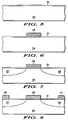
- substrate 10 includes a supporting substrate 12 of gallium arsenide (GaAs) having a plurality of epitaxial layers 13 grown on the surface thereof in any of the techniques utilized in the semiconductor industry.
- Epitaxial layers 13 are crystalographically lattice matched to supporting substrate 12 in a well known manner and cooperate to provide a device commonly known as a heterostructure field effect transistor (HFET).
- HFET heterostructure field effect transistor
- an insulating and passivating layer 15 is positioned on the surface of substrate 10 in overlying relationship to epitaxial layers 13.
- layer 15 is a very thin layer of In x Ga x-1 F 3 , where (0 ⁇ x ⁇ 1). While layer 15 may be grown by any of several methods, in this preferred embodiment it is grown by metalo-organic chemical vapor deposition (MOCVD) or metal-organic molecular beam epitaxy (MOMBE).
- MOCVD metalo-organic chemical vapor deposition
- MOMBE metal-organic molecular beam epitaxy
- substrate 10 is placed in a vacuum chamber and the deposition occurs introducing chemicals to provide the following reaction (CF 3 COCH 2 COCH 3 ) 3 Ga ⁇ GaF 3 + 3C 5 F 2 O 2 H 5 (CF 3 COCH 2 COCH 3 ) 3 In ⁇ InF 3 + 3C 5 F 2 O 2 H 5 .
- layer 15 is lattice matched to substrate 10, in the direction of the basal plane.
- Fluoride usually has a large barrier height: 9.6eV for GaF 3 and 8.15eV for InF 3 , and has very high resistivity (10 12 ohms/cm or above). Fluoride has several other advantages over oxides and nitrides including the fact that fluorine is the most electronegative element and tends to segregate at an interface and tie up dangling bonds at the interface. The correct amount of fluorine at an Si-SiO 2 interface, for example, makes the interface more hot-electron resistant. Also, polysilicon oxide leakage current and breakdown strength are improved as fluorine is incorporated into the oxide film.
- Ga-F, In-F, and As-F are strong bonds which are capable of withstanding short time high temperature annealing (such as that performed after doping implants).
- the advantages of using In x Ga x-1 F 3 are a lower interface state density (i.e. ⁇ 10 11 eV -1 cm -2 ) and better thermal stability since lattice-matched material makes a better interface with the underlying substrate than lattice-mismatched material.
- a gate electrode is deposited on the upper surface in overlying relationship to a gate (or channel) area as illustrated in FIG. 3.
- Other fabrication steps can then be performed, without damaging insulating and passivating layer 15.
- Typical steps are the deposition of source and drain terminals 20 and 21, respectively. Because of the characteristics of insulating and passivating layer 15, discussed above, a passivated surface area is included which provides consistent device operation, improved device characteristics, and better reliability.
- FIGS. 5 - 8 another structure embodying the present invention is illustrated in various simplified cross-sectional views.
- a substrate 30 is provided and an insulating and passivating layer 31 is grown on the upper surface thereof.
- Layer 31 is basically the same as layer 15 of FIG. 2 but may include a slightly different value of x, i.e. a different ratio of GaF 3 to InF 3 .
- a control electrode (e.g. gate, base, etc.) 35 is deposited on the surface of layer 15, as illustrated in FIG. 6, and electrode 35 may then be used as a mask for implanting current carrying electrodes (e.g. source/drain, emitter/collector, etc.) 37 and 38 in substrate 30, as illustrated in FIG. 7.
- current carrying electrodes e.g. source/drain, emitter/collector, etc.
- electrode 35 can be formed and used as a mask for the subsequent self-aligned procedure, including annealing of electrodes 37 and 38.
- external metal contacts 40 and 41 are deposited on substrate 30 in contact with electrodes 37 and 38, respectively, as illustrated in FIG. 8. In some applications it will be desirable to remove portions of layer 31 where contacts 40 and 41 are placed, but in some applications it may not be necessary to perform this extra step, because of the fact that layer 31 is very thin.
- a new and improved method of fabricating semiconductor devices with a passivated surface area is disclosed.
- the new and improved method of fabricating semiconductor devices with a passivated surface area provides consistent device operation, improved device characteristics, and better reliability.
- the new and improved method of fabricating semiconductor devices with a passivated surface area is relatively easy and accurate to perform.
- new and improved semiconductor devices are disclosed which have substantially improved breakdown and reliability characteristics.
Landscapes
- Junction Field-Effect Transistors (AREA)
- Formation Of Insulating Films (AREA)
- Insulated Gate Type Field-Effect Transistor (AREA)
- Thin Film Transistor (AREA)
Applications Claiming Priority (2)
| Application Number | Priority Date | Filing Date | Title |
|---|---|---|---|
| US555674 | 1995-11-13 | ||
| US08/555,674 US5539248A (en) | 1995-11-13 | 1995-11-13 | Semiconductor device with improved insulating/passivating layer of indium gallium fluoride (InGaF) |
Publications (2)
| Publication Number | Publication Date |
|---|---|
| EP0773579A2 true EP0773579A2 (fr) | 1997-05-14 |
| EP0773579A3 EP0773579A3 (fr) | 1997-06-04 |
Family
ID=24218190
Family Applications (1)
| Application Number | Title | Priority Date | Filing Date |
|---|---|---|---|
| EP96117872A Withdrawn EP0773579A3 (fr) | 1995-11-13 | 1996-11-12 | Dispositif semi-conducteur ayant une couche de passivation/isolation améliorée |
Country Status (3)
| Country | Link |
|---|---|
| US (1) | US5539248A (fr) |
| EP (1) | EP0773579A3 (fr) |
| JP (1) | JPH09148580A (fr) |
Families Citing this family (3)
| Publication number | Priority date | Publication date | Assignee | Title |
|---|---|---|---|---|
| US20030058022A1 (en) * | 1999-12-14 | 2003-03-27 | Rajendran Nair | Device and method for controlling voltage variation |
| US7829195B2 (en) * | 2006-12-31 | 2010-11-09 | Intel Corporation | Fluorination pre-treatment of heat spreader attachment indium thermal interface material |
| US20080156635A1 (en) * | 2006-12-31 | 2008-07-03 | Simon Bogdan M | System for processes including fluorination |
Citations (1)
| Publication number | Priority date | Publication date | Assignee | Title |
|---|---|---|---|---|
| US5041393A (en) | 1988-12-28 | 1991-08-20 | At&T Bell Laboratories | Fabrication of GaAs integrated circuits |
Family Cites Families (5)
| Publication number | Priority date | Publication date | Assignee | Title |
|---|---|---|---|---|
| US4368098A (en) * | 1969-10-01 | 1983-01-11 | Rockwell International Corporation | Epitaxial composite and method of making |
| EP0055032B1 (fr) * | 1980-12-23 | 1986-04-23 | National Research Development Corporation | Transistor à effet de champ |
| FR2598030B1 (fr) * | 1986-04-24 | 1990-12-21 | Centre Nat Rech Scient | Procede et dispositif de realisation d'une couche de passivation sur un substrat semiconducteur |
| JPH0196982A (ja) * | 1987-10-08 | 1989-04-14 | Sharp Corp | 半導体レーザ素子 |
| US5051792A (en) * | 1987-10-20 | 1991-09-24 | Bell Communications Research, Inc. | Epitaxial intermetallic contact for compound for compound semiconductors |
-
1995
- 1995-11-13 US US08/555,674 patent/US5539248A/en not_active Expired - Fee Related
-
1996
- 1996-10-30 JP JP8305889A patent/JPH09148580A/ja active Pending
- 1996-11-12 EP EP96117872A patent/EP0773579A3/fr not_active Withdrawn
Patent Citations (1)
| Publication number | Priority date | Publication date | Assignee | Title |
|---|---|---|---|---|
| US5041393A (en) | 1988-12-28 | 1991-08-20 | At&T Bell Laboratories | Fabrication of GaAs integrated circuits |
Also Published As
| Publication number | Publication date |
|---|---|
| JPH09148580A (ja) | 1997-06-06 |
| EP0773579A3 (fr) | 1997-06-04 |
| US5539248A (en) | 1996-07-23 |
Similar Documents
| Publication | Publication Date | Title |
|---|---|---|
| US5506421A (en) | Power MOSFET in silicon carbide | |
| KR920002090B1 (ko) | 전계효과 트랜지스터의 제조방법 | |
| US5384270A (en) | Method of producing silicon carbide MOSFET | |
| JP3217690B2 (ja) | 半導体装置の製造方法 | |
| EP0965145B1 (fr) | Transistor en couche mince a haute tension a caracteristiques d'etat passant ameliorees et son procede de production | |
| EP0064829B1 (fr) | Dispositif à haute mobilité électronique et procédé pour sa fabrication | |
| US5780324A (en) | Method of manufacturing a vertical semiconductor device | |
| EP0492991A2 (fr) | Procédé pour extraire et pour le contrôle de la formation des défauts pendant la fabrication de cellules de circuit intégré à double diffusion et cellule associée | |
| US6858499B2 (en) | Method for fabrication of MOSFET with buried gate | |
| US6194273B1 (en) | Method of manufacturing an insulated gate type semiconductor device having a U-shaped groove | |
| US6025613A (en) | Semiconductor device capable of reducing leak current and having excellent pinch-off characteristic and method of manufacturing the same | |
| EP0746037A2 (fr) | HIGFET du type N et son procédé de fabrication | |
| US5877047A (en) | Lateral gate, vertical drift region transistor | |
| US5539248A (en) | Semiconductor device with improved insulating/passivating layer of indium gallium fluoride (InGaF) | |
| JP2001185717A (ja) | 半導体装置及びその製造方法 | |
| KR100198309B1 (ko) | 쇼트키 접합을 포함하는 반도체 장치 | |
| US5837570A (en) | Heterostructure semiconductor device and method of fabricating same | |
| EP0498993B1 (fr) | Transistor à effet de champ et sa méthode de production | |
| Campbell et al. | Trapezoidal-groove Schottky-gate vertical-channel GaAs FET (GaAs static induction transistor) | |
| KR940010557B1 (ko) | 반도체장치 | |
| US6114195A (en) | Manufacturing method of compound semiconductor field effect transistor | |
| US5693969A (en) | MESFET having a termination layer in the channel layer | |
| JP3277910B2 (ja) | 電界効果トランジスタ及びその製造方法 | |
| JPS62115781A (ja) | 電界効果トランジスタ | |
| JP3018885B2 (ja) | 半導体装置の製造方法 |
Legal Events
| Date | Code | Title | Description |
|---|---|---|---|
| PUAI | Public reference made under article 153(3) epc to a published international application that has entered the european phase |
Free format text: ORIGINAL CODE: 0009012 |
|
| PUAL | Search report despatched |
Free format text: ORIGINAL CODE: 0009013 |
|
| AK | Designated contracting states |
Kind code of ref document: A2 Designated state(s): DE FR GB |
|
| AK | Designated contracting states |
Kind code of ref document: A3 Designated state(s): DE FR GB |
|
| 17P | Request for examination filed |
Effective date: 19971204 |
|
| STAA | Information on the status of an ep patent application or granted ep patent |
Free format text: STATUS: THE APPLICATION HAS BEEN WITHDRAWN |
|
| 18W | Application withdrawn |
Withdrawal date: 19990520 |