EP0773585A2 - Halbleiteranordnung vom Druckkontakttyp - Google Patents
Halbleiteranordnung vom Druckkontakttyp Download PDFInfo
- Publication number
- EP0773585A2 EP0773585A2 EP96308082A EP96308082A EP0773585A2 EP 0773585 A2 EP0773585 A2 EP 0773585A2 EP 96308082 A EP96308082 A EP 96308082A EP 96308082 A EP96308082 A EP 96308082A EP 0773585 A2 EP0773585 A2 EP 0773585A2
- Authority
- EP
- European Patent Office
- Prior art keywords
- emitter
- electrode
- gate electrode
- semiconductor chip
- gate
- Prior art date
- Legal status (The legal status is an assumption and is not a legal conclusion. Google has not performed a legal analysis and makes no representation as to the accuracy of the status listed.)
- Granted
Links
Images



Classifications
-
- H—ELECTRICITY
- H10—SEMICONDUCTOR DEVICES; ELECTRIC SOLID-STATE DEVICES NOT OTHERWISE PROVIDED FOR
- H10W—GENERIC PACKAGES, INTERCONNECTIONS, CONNECTORS OR OTHER CONSTRUCTIONAL DETAILS OF DEVICES COVERED BY CLASS H10
- H10W72/00—Interconnections or connectors in packages
-
- H—ELECTRICITY
- H10—SEMICONDUCTOR DEVICES; ELECTRIC SOLID-STATE DEVICES NOT OTHERWISE PROVIDED FOR
- H10W—GENERIC PACKAGES, INTERCONNECTIONS, CONNECTORS OR OTHER CONSTRUCTIONAL DETAILS OF DEVICES COVERED BY CLASS H10
- H10W76/00—Containers; Fillings or auxiliary members therefor; Seals
- H10W76/10—Containers or parts thereof
- H10W76/12—Containers or parts thereof characterised by their shape
- H10W76/13—Containers comprising a conductive base serving as an interconnection
- H10W76/138—Containers comprising a conductive base serving as an interconnection having another interconnection being formed by a cover plate parallel to the conductive base, e.g. sandwich type
Definitions
- the present invention relates to a pressure-contact type semiconductor device and more particularly to an emitter voltage sensing electrode in MOS gate driving switching devices used in, for instance, IGBT (Insulated Gate Bipolar Transistor), thyristor, etc.
- IGBT Insulated Gate Bipolar Transistor
- Fig. 1 shows a schematic pattern layout on conventional pressure-contact type IGBT chips.
- the cross-sectional structure along the line B-B in Fig. 1 is schematically shown in Fig. 2, and an equivalent circuit of said pressure-contact type IGBT is shown in Fig. 3.
- 60 shows an IGBT chip.
- an emitter electrode array 62 and a gate electrode 63 separately insulated from each other.
- 64 is a chip frame made of electrically insulate material to hold the outer edge of said IGBT chip 60;
- 65 is a first Mo (Molybdenum) plate so arranged that its one side is brought in contact with said emitter electrode array 62 of said IGBT chip 60;
- 66 is a Cu emitter electrode plate so arranged that the other side is brought in compression contact with said first Mo plate 65.
- 67 is a second Mo plate so arranged that its one side is brought in contact with a collector electrode formed on the back of said IGBT chip 60, and 68 is a collector electrode plate so arranged that the other side is brought in compression contact with said second Mo plate 67.
- 69 is a gate electrode pull-out lead wire of which one end is brought in compression contact with a gate electrode 63 of said IGBT chip 60, the other end is taken out to the outside and its middle portion is covered by, for instance, an insulated tube 70 and is passing through a space enclosed by said chip frame 64 and emitter compression contact plates (the first Mo plate 65, the Cu emitter electrode plate 66).
- E is an emitter terminal connected to said Cu emitter electrode plate 66; C is a collector terminal connected to said collector electrode plate 68; and G is a gate terminal connected to said gate electrode lead wire 69.
- an emitter compression contact plate composed of a single Mo plate 65 and a single Cu emitter electrode plate 66 is brought in compression contact with said emitter electrode array 62 on a single chip 60 and a collector compression contact plate composed of a single Mo plate 67 and a single collector electrode plate 68 is brought in compression contact a collector electrode on the back of the chip 60.
- an emitter voltage sensing terminal is needed to sense (monitor) voltage of an emitter electrode of the IGBT in order to detect overcurrent when applied to the IGBT.
- an emitter terminal ES is connected to the Cu emitter electrode plate 66.
- di/dt if di/dt is large, a large induced noise is generated between the emitter terminal and the emitter electrode 62; an error is produced between a measured voltage value of the emitter terminal and a true emitter voltage value of the emitter electrode 62; and it becomes impossible to detect emitter voltage accurately.
- the present invention is made to solve the problem described above and it is an object to provide a pressure-contact type semiconductor device that is capable of detecting emitter voltage accurately even when there exists inductance components of an emitter compression contacted plate between an emitter terminal and an emitter electrode array.
- a pressure-contact type semiconductor device of the present invention includes a semiconductor chip having a gate electrode, an emitter electrode insulated and separated from the gate electrode but at the same potential, and an emitter sensing electrode on the top of the emitter electrode; an emitter compression contact plate in compression contact with the emitter electrode of said semiconductor chip; a collector compression contact plate in compression contact with a collector electrode on the back of said semiconductor chip; a gate electrode pull-out lead wire having one end in compression contact with a gate electrode of said semiconductor chip, the middle portion passing through the space electrically insulated from said emitter compression contact plate and the other end taken out to the outside; and an emitter sensing electrode pull-out lead wire having one end in compression contact with the emitter sensing electrode of said semiconductor chip, the middle portion passing through the space electrically insulated from said emitter compression contact plate, and the other end taken out to the outside.
- a pressure-contact type semiconductor device of the present invention it is possible to detect emitter voltage accurately even when there exists inductance components of an emitter compression contract plate between an emitter terminal and an emitter electrode.
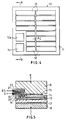
- Fig. 4 is a schematic pattern layout on a pressure-contact type IGBT (Insulated Gate Bipolar Transistor) of withstand voltage about 1700V - 4500V in accordance with a first embodiment of a pressure-contact type semiconductor device of the present invention.
- Fig. 5 shows the cross-sectional structure of this device schematically along the line B-B shown in Fig. 4.
- Fig. 6 shows the cross-sectional structure of the device including an emitter sensing electrode and an emitter electrode along the line C-C shown in Fig. 4.
- Fig. 7 shows an equivalent circuit of the pressure-contact type IGBT shown in Fig. 4.
- an IGBT chip 10 has an emitter electrode 12, an emitter sensing electrode 12a and a gate electrode 13 formed on its top in the shape of an array.
- the width of one emitter electrode (in the vertical direction of the figures) is less than 1.5mm.
- the reason for the arrangement of the emitter electrodes 12 in the shape of array is as follows. That is, the emitter electrode itself has internal resistance and this internal resistance is proportional to the area of the emitter electrode. So, if an emitter electrode is large, its internal resistance also becomes large proportionally and it will become difficult for the IGBT to carry out the high frequency operation.
- Both the emitter electrode 2 and the gate electrode 13 are insulated and separated by an insulation film 11.
- the emitter sensing electrode 12a and the gate electrode 13 are also insulated and separated by the insulation film 11.
- the locations of the emitter sensing electrode 12a and the gate electrode 13 are not especially limited. However, the location of a gate electrode 13a shown in Fig. 6 lies between the emitter electrodes 12 in Fig. 4 and the emitter electrode 12 and the gate electrode 13a are arranged intermittently. The reason for this is that no difference is produced in a time of gate signal provided from gate electrode 13a to reach the gate electrode 13a above the emitter electrode 12. Further, it is desirable that they are formed at close locations to each other (for instance, adjacent locations) in a corner of a region wherein the emitter electrodes 12 are formed. The reason for this will be shown below.
- the first reason is that it is the optimum structure to pull out the emitter electrode and the emitter sensing electrode to the outside in a pressure-contact type structure because the emitter electrode 12 and the emitter sensing electrode 12a are pulled out to the outside by lead wires.
- the second reason is that as the IGBT is of voltage driving type, phases of gate potential and emitter potential will become the same and the gate electrode and the emitter electrode come close to each other and oscillation of their phases is canceled.
- a framework 14 is made of electrically insulated material to hold the outer edge of said IGBT chip 10.
- a first Mo (molybdenum) plate 15 for heat buffering is arranged so that one side of the emitter electrode 12 of said IGBT chip 10 is brought in compression contact with it.
- a Cu (Copper) emitter plate 16 is arranged so that its other side is brought in compression contact with said first Mo plate 15. That is, an emitter compression contact plate composed of a single first Mo plate 15 and a single Cu emitter electrode plate 16 is kept in compression contact with the emitter electrode on a single IGBT chip 10.
- a second Mo plate 17 for heat buffering is arranged so that its one side is in compression contact with a collector electrode formed on the back of said IGBT chip 10.
- a collector electrode plate 18 is arranged so that its other side is in compression contact with the second Mo plate 17. That is, a collector compression contact plate composed of a single second Mo plate 17 and a single collector electrode plate 18 is kept in compression contact with a collector electrode formed on the back of the IGBT chip 10.
- a gate electrode pull-out lead wire 19 has one end in compression contact with the gate electrode 13 of said IGBT chip 10, the other end taken out to the outside, and the middle portion covered by, for instance, an insulation tube 20 and passing through a so-called first space enclosed by said framework 14 and said emitter compression contact plate (the first Mo plate 15, the Cu emitter electrode plate 16).
- an emitter sensing electrode lead wire 26 has one end in compression contact with the emitter sensing electrode 12a of said IGBT chip 10 and the other end taken out to the outside. Its middle portion is covered by, for instance, an insulating tube 22 and passes through the space enclosed by said framework 14 and said emitter compression contact plate (the first Mo plate 15, the Cu emitter electrode plate 16).
- an emitter terminal E is connected to said Cu emitter electrode plate 16.
- a collector terminal C is connected to said collector electrode plate 18.
- a gate terminal G is connected to said gate electrode pull-out lead wire 19.
- An emitter voltage sensing terminal ES is connected to said emitter sensing electrode pull-out lead wire 21.
- Fig. 7 is an enlarged diagram of the dotted portion shown in fig. 5.
- the second Mo plate 17 is electrically connected to a collector layer 31 via a collector electrode 19a and transmits and radiates heat generated in the IGBT chip 10.
- An NPN transistor is composed of an N - layer 32, a base region 33 and emitter region 38, while a PNP transistor is composed of a collector layer 31, an N - layer 32 and a base region 33.
- a thyristor structure is formed by connecting these NPN and PNP transistors in reverse parallel.
- a plurality of the base regions 33 are formed on the top of the N - layer 32.
- the emitter regions 37, 38 are formed on the surface of this base region 33.
- These emitter region 38 and the N - layer 32 construct a source region and a drain region.
- a gate electrode 35 is formed to extend over these emitter region 38 and the N - layer 32 via a gate insulation film 34.
- the gate electrode 35 is pulled out to the outside by a gate electrode pad 13.
- This gate electrode pad 13 is connected to the gate electrode pull-out lead wire 19 and a gate voltage signal is applied to the gate electrode 35 from the outside via this gate electrode pull-out lead wire 19.
- the emitter region 38 is connected to the emitter electrode 12 formed on the surface of the base region 33.
- the emitter electrode 37 although not illustrated, is electrically connected to the emitter region 38 and the emitter sensing electrode 12a. This emitter sensing electrode 12a is pulled out to the outside by the emitter sensing electrode pull-out lead wire 21 and monitors emitter voltage.
- Fig. 6 is a cross-sectional view along the line C-C in Fig. 4.
- the emitter sensing electrode 12a and the emitter electrode 12 are formed on the same layer of a semiconductor substrate which becomes the basic body of the IGBT chip 10 so that they retain the same potential. Further, the emitter electrode 12 is formed in the mesa shape at its upper part and the first Mo plate 15 is brought in compression contact with this part and thus, the first Mo plate 15 and the emitter electrode 12 are electrically connected to each other. Heat generated in the IGBT chip 10 is conducted from the emitter electrode 12 to the first Mo plate 15 and radiated therefrom via the Cu emitter electrode plate.
- the IGBT chip shown in Fig. 6 has a number of IGBT devices which jointly connect to the collector electrode 10a and the emitter sensing electrode 12a connected to the emitter electrode 12.
- the base region 33 is formed at the lower part of the emitter sensing electrode 12a.
- the emitter region 38 is not formed, and the emitter sensing electrode 12a is not in contact with the emitter region 38.
- 31 is an N - type semiconductor layer (the collector layer) and 32 is an N - type semiconductor layer on the P - type semiconductor layer.
- 33 is a P+ type semiconductor layer (the base region) partially formed on the surface of the N - type semiconductor layer 32. The width of this P+ type semiconductor layer 33 is about 3 um and the space between the base regions is about 3-4 um.
- a gate insulation film 34 (oxidized film) is formed on a part of the surface of the N - type semiconductor layer 32. The thickness of this gate insulation film 34 is about 100 nm.
- a gate electrode 35 is formed on the gate insulation film 34 in thickness of about 500 nm.
- 36 is a layer insulation film formed by silicon oxide.
- An electrode 37 for emitter is formed on the layer insulation film 36 using, for instance, an aluminum film. This electrode 37 for emitter is about 4 um thick.
- An insulation film 11 is protecting the gate electrode 13, and separating the emitter electrode 12 from emitter sensing electrode 12a.
- the emitter region 38 is partially formed on the surface of the P+ type semiconductor layer 33 positioned at the lower part of the emitter electrode 12 and the emitter electrode 12 is in contact with this emitter region 38 through a contact hole opened on the layer insulation film 36.
- the emitter region 38 is not formed on the P+ type semiconductor layer 33 positioned at the lower part of the emitter sensing electrode 12a.
- the pressure-contact type IGBT in said structure is equipped with a semiconductor chip 10 provided with a group of the emitter electrodes 12, the emitter sensing electrodes 12a and the gate electrodes 13 formed on the top and divided into the plural numbers by the insulation films 11 and the collector electrodes 10a formed on the back, the chip frame 14 made of electrically insulated material to hold the outer edge of said semiconductor chip; the first heat buffering plate 15 so arranged that one side is brought in pressure contact with the emitter electrode of said semiconductor chip, the emitter electrode plate 16 so arranged that the other side is brought in pressure contact with said first heat buffering plate; the second heat buffering plate 17 so arranged that one side is brought in compression contact with the collector electrode on the back of said semiconductor chip; the collector electrode plate 18 so arranged that the other side is brought in compression contact said second heat buffering plate, the gate electrode pull-out lead wire 19 of which one end is brought in compression contact with the gate electrode of said semiconductor chip, its middle portion will pass through the space which is electrically insulated from said first heat buffering plate and said
- said pressure-contact type IGBT when sensing (monitoring) voltage of the emitter electrode 12 of the IGBT in order to detect an overcurrent and the like of the IGBT in a system using the IGBT, it is possible to directly measure voltage of the emitter sensing electrode 12a via the emitter voltage sensing terminal ES without using the emitter compression contact plate (the first heat buffering plate 15, the emitter electrode plate 16) and the emitter terminal E as in a conventional example.
- Fig. 9 is a diagram corresponding to Fig. 5 in a second embodiment.
- the gate electrode pull-out lead wire 19 and the emitter sensing electrode pull-out lead wire 21 are arranged close to each other in the vertical direction.
- the gate electrode pull-out lead wire 19 and the emitter sensing electrode pull-out lead wire 21 are arranged close to each other in the horizontal direction.
- Fig. 10 is a diagram corresponding to Fig. 5 in a third embodiment.
- the gate electrode pull-out lead wire 19 and the emitter sensing electrode pull-out lead wire 21 are arranged close to each other in the vertical direction.
- the gate electrode pull-out lead wire 19 and the emitter sensing electrode pull-out lead wire 21 are pulled out to the outside in a twisted state.
- the embodiments so far presented are those for a single IGBT chip.
- the concept in the embodiments so far presented is applied to a plurality of IGBT chips.
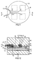
- Fig. 11 is a plan view showing the state of the first Mo plate 15 and the Cu emitter electrode plate 16 compression contacted to a plurality of IGBT chips 10 arranged in a quadrilateral shape as viewed from above.
- Fig. 12 is a cross-sectional view along the line A-A in Fig. 11.
- the IGBT chip 10 On the surface of the IGBT chip 10, there are formed a gate electrode, an emitter electrode which has the same potential as that of the gate electrode, and an emitter sensing electrode. A collector electrode is formed on the back.
- the chip frame 15 made of electrically insulated material is arranged to hold the IGBT chip 10.
- the first Mo plate 15 On each top of a plurality of IGBT chips 10, the first Mo plate 15 is arranged, and these first Mo plates 15 are compression contacted to respective IGBT chips 10 by a single Cu emitter electrode plate 16.
- a plurality of these gate electrode pull-out lead wires 19 and emitter sensing electrode pull-out lead wires 21 are collected together for the gate electrode pull-out lead wires and the emitter sensing electrode pull-out lead wires near respective terminals and pulled out to the outside.
Landscapes
- Semiconductor Integrated Circuits (AREA)
- Thyristors (AREA)
- Measuring Fluid Pressure (AREA)
- Bipolar Transistors (AREA)
Applications Claiming Priority (2)
| Application Number | Priority Date | Filing Date | Title |
|---|---|---|---|
| JP7289880A JPH09135023A (ja) | 1995-11-08 | 1995-11-08 | 圧接型半導体装置 |
| JP289880/95 | 1995-11-08 |
Publications (3)
| Publication Number | Publication Date |
|---|---|
| EP0773585A2 true EP0773585A2 (de) | 1997-05-14 |
| EP0773585A3 EP0773585A3 (de) | 1998-09-09 |
| EP0773585B1 EP0773585B1 (de) | 2006-03-22 |
Family
ID=17748973
Family Applications (1)
| Application Number | Title | Priority Date | Filing Date |
|---|---|---|---|
| EP96308082A Expired - Lifetime EP0773585B1 (de) | 1995-11-08 | 1996-11-07 | Halbleiteranordnung vom Druckkontakttyp |
Country Status (4)
| Country | Link |
|---|---|
| US (1) | US5874750A (de) |
| EP (1) | EP0773585B1 (de) |
| JP (1) | JPH09135023A (de) |
| DE (1) | DE69635946T2 (de) |
Cited By (2)
| Publication number | Priority date | Publication date | Assignee | Title |
|---|---|---|---|---|
| GB2332092A (en) * | 1997-12-08 | 1999-06-09 | Westcode Semiconductors Limite | Encapsulating semiconductor chips |
| CN105283951A (zh) * | 2013-06-11 | 2016-01-27 | 株式会社电装 | 半导体装置 |
Families Citing this family (6)
| Publication number | Priority date | Publication date | Assignee | Title |
|---|---|---|---|---|
| JP3480811B2 (ja) * | 1997-07-15 | 2003-12-22 | 株式会社東芝 | 電圧駆動型電力用半導体装置 |
| CN100418216C (zh) * | 2004-11-30 | 2008-09-10 | 株式会社东芝 | 半导体封装及半导体模块 |
| CN103515365B (zh) * | 2013-10-14 | 2016-04-20 | 国家电网公司 | 一种大功率压接式igbt器件 |
| JP6438839B2 (ja) * | 2015-05-18 | 2018-12-19 | 株式会社日立製作所 | 半導体装置およびそれを用いた電力変換装置 |
| WO2023080081A1 (ja) * | 2021-11-05 | 2023-05-11 | ローム株式会社 | 半導体装置 |
| JP7803811B2 (ja) | 2022-08-10 | 2026-01-21 | 株式会社東芝 | 半導体パッケージ |
Family Cites Families (10)
| Publication number | Priority date | Publication date | Assignee | Title |
|---|---|---|---|---|
| IE55753B1 (en) * | 1983-09-06 | 1991-01-02 | Gen Electric | Power semiconductor device with main current section and emulation current section |
| JP2739970B2 (ja) * | 1988-10-19 | 1998-04-15 | 株式会社東芝 | 圧接型半導体装置 |
| US4965710A (en) * | 1989-11-16 | 1990-10-23 | International Rectifier Corporation | Insulated gate bipolar transistor power module |
| DE69032084T2 (de) * | 1989-11-17 | 1998-07-16 | Toshiba Kawasaki Kk | Halbleiteranordnung mit zusammengesetzter Bipolar-MOS-Elementpille, geeignet für eine Druckkontaktstruktur |
| DE4216810C2 (de) * | 1991-05-31 | 1999-09-16 | Fuji Electric Co Ltd | Steuerschaltung für einen Leitfähigkeitsänderungs-MISFET |
| US5337214A (en) * | 1993-05-03 | 1994-08-09 | Eaton Corporation | Bypass contactor for solid state motor starters |
| JP3180863B2 (ja) * | 1993-07-27 | 2001-06-25 | 富士電機株式会社 | 加圧接触形半導体装置およびその組立方法 |
| JPH07161992A (ja) * | 1993-10-14 | 1995-06-23 | Fuji Electric Co Ltd | 絶縁ゲート型バイポーラトランジスタ |
| JP3471880B2 (ja) * | 1994-02-23 | 2003-12-02 | 三菱電機株式会社 | 圧接型半導体装置 |
| US5596466A (en) * | 1995-01-13 | 1997-01-21 | Ixys Corporation | Intelligent, isolated half-bridge power module |
-
1995
- 1995-11-08 JP JP7289880A patent/JPH09135023A/ja not_active Abandoned
-
1996
- 1996-11-06 US US08/743,812 patent/US5874750A/en not_active Expired - Lifetime
- 1996-11-07 DE DE69635946T patent/DE69635946T2/de not_active Expired - Lifetime
- 1996-11-07 EP EP96308082A patent/EP0773585B1/de not_active Expired - Lifetime
Non-Patent Citations (1)
| Title |
|---|
| None |
Cited By (5)
| Publication number | Priority date | Publication date | Assignee | Title |
|---|---|---|---|---|
| GB2332092A (en) * | 1997-12-08 | 1999-06-09 | Westcode Semiconductors Limite | Encapsulating semiconductor chips |
| US6303974B1 (en) | 1997-12-08 | 2001-10-16 | Westcode Semiconductors Limited | Semiconductor chips encapsulated within a preformed sub-assembly |
| GB2332092B (en) * | 1997-12-08 | 2002-10-23 | Westcode Semiconductors Ltd | Encapsulating semiconductor chips |
| CN105283951A (zh) * | 2013-06-11 | 2016-01-27 | 株式会社电装 | 半导体装置 |
| CN105283951B (zh) * | 2013-06-11 | 2018-04-03 | 株式会社电装 | 半导体装置 |
Also Published As
| Publication number | Publication date |
|---|---|
| DE69635946T2 (de) | 2006-12-14 |
| DE69635946D1 (de) | 2006-05-11 |
| EP0773585B1 (de) | 2006-03-22 |
| US5874750A (en) | 1999-02-23 |
| EP0773585A3 (de) | 1998-09-09 |
| JPH09135023A (ja) | 1997-05-20 |
Similar Documents
| Publication | Publication Date | Title |
|---|---|---|
| US7969000B2 (en) | Semiconductor device | |
| JP2973588B2 (ja) | Mos型半導体装置 | |
| EP1028467B1 (de) | Aktive Halbleitersicherung für eine Wechselstromleitung und Zweiwegschaltervorrichtung für die Sicherung | |
| US4314268A (en) | Integrated circuit with shielded lead patterns | |
| EP0738011B1 (de) | Integrierter Hochspannungsschaltkreis, Hochspannungsübergangsabschluss- struktur und MIS-Hochspannungstransistor | |
| WO1999004433A2 (en) | Mcm semiconductor device assemblies and circuits | |
| US5530277A (en) | Insulated-gate bipolar transistor | |
| US5633525A (en) | Lateral field effect transistor | |
| EP0494597A1 (de) | Leistungshalbleiteranordnung mit einer Graben-Gateelektrode | |
| US5874750A (en) | Pressure-contact type semiconductor device | |
| JP2987088B2 (ja) | Mos技術電力デバイスチィップ及びパッケージ組立体 | |
| US5497013A (en) | Semi-conductor chip having interdigitated gate runners with gate bonding pads | |
| EP0139998A1 (de) | Leistungshalbleiteranordnung mit einem Haupt- und einem Nebenstromabschnitt | |
| JPH10247718A (ja) | 電流検知部付き縦型半導体素子 | |
| JP2025514117A (ja) | オンチップ電流センサの動的性能 | |
| US6133616A (en) | Tempsense FET with implanted line of diodes (EPS) | |
| EP0834927A2 (de) | Halbleiter-IC-Anordnung | |
| JP3383451B2 (ja) | 半導体装置 | |
| US7368825B2 (en) | Power semiconductor device | |
| US8530930B2 (en) | Semiconductor device having plural insulated gate switching cells and method for designing the same | |
| JPH0729933A (ja) | 電力用半導体装置 | |
| US4998160A (en) | Substrate power supply contact for power integrated circuits | |
| US20240332137A1 (en) | Electronic device | |
| CN111273073B (zh) | Igbt芯片及半导体功率模块 | |
| KR100259726B1 (ko) | 반도체 장치 |
Legal Events
| Date | Code | Title | Description |
|---|---|---|---|
| PUAI | Public reference made under article 153(3) epc to a published international application that has entered the european phase |
Free format text: ORIGINAL CODE: 0009012 |
|
| 17P | Request for examination filed |
Effective date: 19961206 |
|
| AK | Designated contracting states |
Kind code of ref document: A2 Designated state(s): DE FR GB |
|
| PUAL | Search report despatched |
Free format text: ORIGINAL CODE: 0009013 |
|
| RHK1 | Main classification (correction) |
Ipc: H01L 29/739 |
|
| AK | Designated contracting states |
Kind code of ref document: A3 Designated state(s): DE FR GB |
|
| 17Q | First examination report despatched |
Effective date: 19991104 |
|
| GRAP | Despatch of communication of intention to grant a patent |
Free format text: ORIGINAL CODE: EPIDOSNIGR1 |
|
| GRAS | Grant fee paid |
Free format text: ORIGINAL CODE: EPIDOSNIGR3 |
|
| GRAA | (expected) grant |
Free format text: ORIGINAL CODE: 0009210 |
|
| AK | Designated contracting states |
Kind code of ref document: B1 Designated state(s): DE FR GB |
|
| REG | Reference to a national code |
Ref country code: GB Ref legal event code: FG4D |
|
| REF | Corresponds to: |
Ref document number: 69635946 Country of ref document: DE Date of ref document: 20060511 Kind code of ref document: P |
|
| ET | Fr: translation filed | ||
| PLBE | No opposition filed within time limit |
Free format text: ORIGINAL CODE: 0009261 |
|
| STAA | Information on the status of an ep patent application or granted ep patent |
Free format text: STATUS: NO OPPOSITION FILED WITHIN TIME LIMIT |
|
| 26N | No opposition filed |
Effective date: 20061227 |
|
| PGFP | Annual fee paid to national office [announced via postgrant information from national office to epo] |
Ref country code: FR Payment date: 20101123 Year of fee payment: 15 |
|
| PGFP | Annual fee paid to national office [announced via postgrant information from national office to epo] |
Ref country code: DE Payment date: 20101104 Year of fee payment: 15 |
|
| PGFP | Annual fee paid to national office [announced via postgrant information from national office to epo] |
Ref country code: GB Payment date: 20101103 Year of fee payment: 15 |
|
| GBPC | Gb: european patent ceased through non-payment of renewal fee |
Effective date: 20111107 |
|
| REG | Reference to a national code |
Ref country code: FR Ref legal event code: ST Effective date: 20120731 |
|
| REG | Reference to a national code |
Ref country code: DE Ref legal event code: R119 Ref document number: 69635946 Country of ref document: DE Effective date: 20120601 |
|
| PG25 | Lapsed in a contracting state [announced via postgrant information from national office to epo] |
Ref country code: GB Free format text: LAPSE BECAUSE OF NON-PAYMENT OF DUE FEES Effective date: 20111107 |
|
| PG25 | Lapsed in a contracting state [announced via postgrant information from national office to epo] |
Ref country code: FR Free format text: LAPSE BECAUSE OF NON-PAYMENT OF DUE FEES Effective date: 20111130 |
|
| PG25 | Lapsed in a contracting state [announced via postgrant information from national office to epo] |
Ref country code: DE Free format text: LAPSE BECAUSE OF NON-PAYMENT OF DUE FEES Effective date: 20120601 |