EP0773607A2 - Connecteur de bord de carte - Google Patents
Connecteur de bord de carte Download PDFInfo
- Publication number
- EP0773607A2 EP0773607A2 EP96117589A EP96117589A EP0773607A2 EP 0773607 A2 EP0773607 A2 EP 0773607A2 EP 96117589 A EP96117589 A EP 96117589A EP 96117589 A EP96117589 A EP 96117589A EP 0773607 A2 EP0773607 A2 EP 0773607A2
- Authority
- EP
- European Patent Office
- Prior art keywords
- spring contact
- board
- edge
- contact elements
- slot
- Prior art date
- Legal status (The legal status is an assumption and is not a legal conclusion. Google has not performed a legal analysis and makes no representation as to the accuracy of the status listed.)
- Withdrawn
Links
- 230000013011 mating Effects 0.000 claims abstract description 20
- 238000003780 insertion Methods 0.000 claims description 14
- 229910000679 solder Inorganic materials 0.000 claims description 14
- 230000037431 insertion Effects 0.000 claims description 10
- 230000003247 decreasing effect Effects 0.000 claims description 3
- 239000007769 metal material Substances 0.000 description 3
- 238000005476 soldering Methods 0.000 description 2
- 230000005540 biological transmission Effects 0.000 description 1
- 238000010276 construction Methods 0.000 description 1
- 239000003989 dielectric material Substances 0.000 description 1
- 238000004519 manufacturing process Methods 0.000 description 1
- 239000000463 material Substances 0.000 description 1
- 239000002184 metal Substances 0.000 description 1
- 238000005192 partition Methods 0.000 description 1
Images
Classifications
-
- H—ELECTRICITY
- H01—ELECTRIC ELEMENTS
- H01R—ELECTRICALLY-CONDUCTIVE CONNECTIONS; STRUCTURAL ASSOCIATIONS OF A PLURALITY OF MUTUALLY-INSULATED ELECTRICAL CONNECTING ELEMENTS; COUPLING DEVICES; CURRENT COLLECTORS
- H01R12/00—Structural associations of a plurality of mutually-insulated electrical connecting elements, specially adapted for printed circuits, e.g. printed circuit boards [PCB], flat or ribbon cables, or like generally planar structures, e.g. terminal strips, terminal blocks; Coupling devices specially adapted for printed circuits, flat or ribbon cables, or like generally planar structures; Terminals specially adapted for contact with, or insertion into, printed circuits, flat or ribbon cables, or like generally planar structures
- H01R12/70—Coupling devices
- H01R12/7005—Guiding, mounting, polarizing or locking means; Extractors
-
- H—ELECTRICITY
- H01—ELECTRIC ELEMENTS
- H01R—ELECTRICALLY-CONDUCTIVE CONNECTIONS; STRUCTURAL ASSOCIATIONS OF A PLURALITY OF MUTUALLY-INSULATED ELECTRICAL CONNECTING ELEMENTS; COUPLING DEVICES; CURRENT COLLECTORS
- H01R12/00—Structural associations of a plurality of mutually-insulated electrical connecting elements, specially adapted for printed circuits, e.g. printed circuit boards [PCB], flat or ribbon cables, or like generally planar structures, e.g. terminal strips, terminal blocks; Coupling devices specially adapted for printed circuits, flat or ribbon cables, or like generally planar structures; Terminals specially adapted for contact with, or insertion into, printed circuits, flat or ribbon cables, or like generally planar structures
- H01R12/70—Coupling devices
- H01R12/71—Coupling devices for rigid printing circuits or like structures
- H01R12/72—Coupling devices for rigid printing circuits or like structures coupling with the edge of the rigid printed circuits or like structures
- H01R12/721—Coupling devices for rigid printing circuits or like structures coupling with the edge of the rigid printed circuits or like structures cooperating directly with the edge of the rigid printed circuits
Definitions
- This invention generally relates to the art of electrical connectors and, particularly, to a high-speed edge connector for a printed circuit board.
- an edge card connector is provided for receiving a printed circuit board having a mating edge and a plurality of contact pads adjacent the edge.
- Such edge card connectors having an elongated housing defining an elongated slot for receiving the mating edge of the printed circuit board.
- a plurality of terminals are spaced along one or both sides of the slot for engaging the contact pads adjacent the mating edge of the board.
- the terminals have some form or another of spring contact elements for biased engagement against the contact pads of the board and, most often, the spring contact elements are in one form or another of a cantilevered spring arm.
- the present invention is directed to further improvements in edge card connectors, including improved biasing means for biasing the printed circuit board, as well as improved latch means for the printed circuit board.
- An object, therefore, of the invention is to provide a new and improved edge card connector for a printed circuit board having a mating edge and a plurality of contact pads adjacent the edge.
- the edge card connector includes a dielectric housing having a board-receiving slot for receiving the edge of the printed circuit board.
- a plurality of spring contact elements are mounted in the housing along at least one side of the slot.
- the spring contact elements have spring contact portions extending into the slot for contacting respective ones of the contact pads on the printed circuit board.
- the housing includes surface means at one side of the slot defining a datum plane beyond which the spring contact portion of at least one of the spring contact elements extends into the slot.
- Biasing means is provided in the housing for biasing the printed circuit board against the surface means, thereby deflecting the spring contact portion of at least one spring contact element a predetermined amount.
- the biasing means is provided by a second spring contact portion extending into the slot for contacting the printed circuit board on a side opposite the one side of the board and biasing the one side of the board against the datum plane and the first spring contact portion.
- the second spring contact portion is generally C-shaped and extends from a base portion of the spring contact portion in a generally uniformly decreasing cross-section from a relatively wide base end at the base portion to a relatively narrow distal end for contacting the printed circuit board.
- the generally C-shaped second spring contact portion has a generally circular inside edge and a generally circular outside edge formed on a larger radius than the inside edge, and with the centers of curvature of the edges being offset.
- the distal end of the generally C-shaped second spring contact portion has an outwardly flared tip to assist in guiding the mating edge of the printed circuit board between the first and second spring contact portions.
- the spring contact elements include ground contact elements and signal contact elements respectively alternating lengthwise of the board-receiving slot.
- the spring contact elements have board-mounting feet projecting from the elongated housing generally in a line therealong.
- the board-mounting feet of the ground contact elements are larger than the board-mounting feet of the signal contact elements to provide a shielding means for the signal contact elements.
- the board-mounting feet of the spring contact elements comprise right-angled surface-mount solder tails.
- Another feature of the invention involves the provision of the base portions of at least some of the spring contact elements with tool-engaging shoulder means.
- the shoulder means are adapted for engagement by an appropriate contact insertion tool.
- the spring contact elements each include a barb insertable into a mounting hole in the housing.
- the tool-engaging shoulder is generally aligned with the barb in a contact-insertion direction.
- the edge connector also includes a pair of board latches mounted at the opposite ends of the housing and including board-lock means for lockingly engaging opposite sides of the printed circuit board when the board is inserted into the board-receiving slot. It is contemplated that the pair of latches are identical and interchangeable at opposite ends of the housing to reduce manufacturing and inventory expenses.
- the board latches are mounted to the outsides of the opposite ends of the housing, with the board-lock means projecting to the inside of the housing.
- the board latches are stamped and formed of sheet metal material and include first ends fixed to the housing and free ends resiliently movable relative to the housing.
- the board lock means are located near the free ends.
- Anti-overstress means are provided at the free ends to limit the resilient movement of the free ends of the board latches.
- an edge connector for receiving a printed circuit board (not shown) having a mating edge and a plurality of contact pads adjacent the edge.
- edge card connectors in that they have receptacle means in the form of slots for allowing insertion of an edge of printed circuit boards into contact areas of the connectors.
- Such connectors are well known in the industry as exemplified by U.S. Patent Nos. 4,575,172 and 5,203,725, assigned to the assignee of this invention.
- Such connectors are elongated and have rows of spring contact elements spaced along one or both sides of an elongated card-receiving slot extending lengthwise of a dielectric housing.
- the spring contact elements engage contact pads spaced along a mating edge of the printed circuit board which is inserted into the slot.
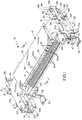
- edge connector 10 includes a dielectric housing, generally designated 12, having a board-receiving slot 14 running the length of the connector between opposite ends 16 of the housing.
- the housing in essence, defines a terminating face 18 and a board-receiving face 20, with slot 14 opening at the board-receiving face.
- a plurality of mounting pegs 22 depend from housing 12 for insertion into appropriate mounting holes of a second printed circuit board (now shown). Often, the second printed circuit board is called a mother board and the printed circuit board which is inserted into slot 14 is called a daughter board.
- a pair of wings 24 project rearwardly of the housing at opposite ends 16 thereof.
- a board latch, generally designated 16 is mounted on the outside of each wing 24 at each opposite end of the housing.
- a pair of metal fitting nails 28 are mounted in housing 12 and project rearwardly of the board-receiving face and include solder feet 30 for securement to solder pads on the mother board.
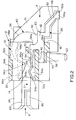
- housing 12 includes a plurality of transverse cavities, generally designated 32, spaced longitudinally of slot 14 for receiving alternating, differently configured terminals, as described below.
- each cavity 32 has a cavity portion 32a on one side of slot 14 (the bottom side as viewed in Figure 2) and a cavity portion 32b on the opposite side of the slot (the top side as viewed in Fig. 2).
- Cavities 32 are separated lengthwise of the elongated housing by wall means or partitions which include wall portions 34a separating cavity portions 32a and wall portions 34b separating cavity portions 32b.
- Housing 12 also includes a plurality of holes 36 (Fig. 2) outside cavities 32 and generally in transverse alignment therewith, for purposes described hereinafter.
- Each hole 36 includes a mouth 36a opening at the terminating face 18 of the housing.
- the entire housing is unitarily molded of dielectric material such as plastic or the like.
- a plurality of terminals are mounted in housing 12, spaced longitudinally of the housing and corresponding to the plurality of transversely aligned cavities 32 and holes 36.
- the printed circuit board which is inserted into slot 14 often has a plurality of contact pads defining two rows of pads parallel to and generally along the edge of the printed circuit board, i.e. the mating edge which is inserted into the slot.
- One row of contact pads is located near the absolute edge of the board, and the other row of contact pads is spaced inwardly from the one row. Therefore, conventionally, terminals are located on housing 12 with contact elements alternating lengthwise of the housing for alternatingly engaging the contact pads in the two rows thereof along the mating edge of the printed circuit board.
- terminals are mounted in housing 12 in an alternating array lengthwise of the housing.
- terminals 38 alternate between adjacent terminals 40, and vice versa.
- Terminals 38 are signal terminals within edge connector 10
- terminals 40 are ground/power terminals within the connector.
- Both configurations of terminals 38 and 40 are similar to the extent that they have base portions 42 and barb portions 44 projecting forwardly from the base portions.
- the terminals are mounted to housing 12 by inserting barb portions 44 through mouths 36a of holes 36 from terminating face 18 of the housing to create an interference fit between the barbs and the side walls of their respective holes.
- serrations 46 are formed in one or both edges of barbs 44 to bight into the plastic material of the housing at the side walls of holes 36.
- signal terminals 38 have board-mounting feet 48 in the form of right-angled solder tails extending outwardly and downwardly from the base portions 42 of the terminals.
- the solder tails terminate in surface mount portions 48a for soldering to appropriate signal circuit traces on the mother board.
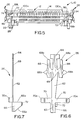
- Signal terminals 38 also have cantilevered spring contact elements 50 projecting from their respective base portions 42 into cavity portions 32a. Each spring contact element 50 has a contact point 50a which projects from cavity portion 32a into slot 14.
- each ground/power terminal 40 also includes a board-mounting foot 52 in the form of a right-angled solder tail portion projecting outwardly and downwardly from the respective base portion 42 of the terminal.
- the solder tail terminates in a surface mount portion 52a for soldering to an appropriate ground/power circuit trace on the mother board.
- Each terminal 40 also includes a cantilevered spring contact element 54 projecting from the base portion 42 into a respective one of the cavity portions 32a alternating with the cavity portions 32a into which the spring contact elements 50 of terminals 38 project.
- Each spring contact element 54 includes a contact point 54a projecting into slot 14.
- spring contact element 50 of terminal 38 is longer than spring contract element 54 of terminal 40. Regardless, it can be seen in Figure 2 that both configurations of spring contact elements 50 and 54 project into slot 14 for engaging the contact pads along the mating edge of the printed circuit board (daughter board) inserted into slot 14 in the direction of arrow "B" (Fig. 2).
- housing 12 be provided with surface means along the side of slot 14 from which spring contact elements 50 and 54 project, to define a datum plane beyond which contact points 50a and 54a project into the slot.
- biasing means are provided for biasing the printed circuit board against the surface means, thereby deflecting the spring contact elements 50 and 54 a constant and predetermined amount.
- wall portions 34a between cavity portions 32a have edges 56 which are in alignment lengthwise of housing 12 and which define one side (the bottom side as viewed in the drawings) of slot 14. These edges combine to define the datum plane beyond which contact points 50a and 54a of spring contact elements 50 and 54, respectively, project as seen in Figure 2. Therefore, it can be understood that if the daughter printed circuit board is biased against the datum plane in the direction of arrow "C", the datum plane provides an abutment or stop means to prevent further movement of the board and further deflection of the spring contact elements. Once the board engages the datum plane defined by edges 56 of wall portions 34a, the spring contact elements cannot be deflected any further. Consequently, the deflection of the spring contact elements is predetermined and constant. Other aspects of this concept can be derived from the aforementioned U.S. Patent No. 5,203,725.
- each ground terminal 40 has a second spring contact portion 58 extending from base portion 42 into a respective one of the cavity portions 32b and then downwardly into slot 14.
- the second spring contact portion is effective for contacting the daughter printed circuit board on a side thereof opposite the side which engages spring contact elements 50 and 54 and biasing the board against datum plane 56 while deflecting the spring contact elements 50 and 54.
- each ground terminal 40 is a monolithic structure including spring contact element or portion 54 and second spring contract portion 58.
- the second spring contact portion is generally C-shaped and extends from base portion 42 in a generally uniformly decreasing cross-section from a relatively wide base end 58a at base portion 42 to a relatively narrow distal end 58b for contacting the daughter printed circuit board and biasing the board toward datum plane 56.
- Geometrically, generally C-shaped second spring contact portion 58 has a generally circular inside edge 58c and a generally circular outside edge 58d. The circular outside edge is formed on a larger radius than the circular inside edge, as can be seen.
- an outwardly flared tip 58e is formed at distal end 58b, opposite an opposing outwardly flared tip 54b of spring contact element or portion 54, to assist in guiding the mating edge of the printed circuit board between the two spring contact portions.
- FIG. 2 A feature of the invention is shown in Figure 2 wherein it can be seen that board-mounting foot or solder tail 52 of ground terminal 40 is significantly larger than board-mounting foot or solder tail 48 of signal terminal 38.
- the larger solder tails of the ground terminals provide an effective shielding means for the smaller solder tails of the signal terminals.
- each of terminals 38 and 40 are provided with a tab or boss 60 projecting rearwardly of base portion 42 opposite the insertion direction of arrow "A" (Fig. 2).
- the tabs define shoulder means 60a adapted for engagement by an appropriate contact insertion tool. It can be seen that the shoulder means is generally aligned with barb 44 in the contact insertion direction of arrow "A". Therefore, the insertion tool will drive barb 44 into its respective hole 36 in the housing without a tendency to twist or skew the terminal during insertion.
- FIGS. 2 and 5 show that housing 12 has a pair of rearwardly extending walls 61 at opposite ends of the array of solder tails 48 and 50. These walls not only stabilize the housing, but they protect the solder tails.
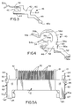
- each universal board latch 26 includes an elongated body 62 having a snap-latch head 64 at one end thereof and a board-lock flange 66 at the opposite or free end 67 of the body. Head 64 is coplanar with the body, and flange 66 projects transversely of or perpendicular to the body.
- a pair of retaining arms 68 are formed coplanar with the body at opposite edges thereof near head 64.
- a pair of operating arms 70 are formed coplanar with the body near board-lock flange 66.
- the operating arms have distal ends 70a that are bent outwardly as best seen in Figures 1 and 8 to define finger tabs which facilitate manual grasping by an operator.
- an anti-overstress tab 72 projects transversely of board-lock flange 66 at an inner end thereof. It can be seen in Figure 5 that the anti-overstress tab 72 of the left-hand board latch 26 projects upwardly, while the anti-overstress tab 72 of the right-hand board latch projects downwardly. This shows the universal nature of the board-latches.
- the corners of the board engage a chamfered or angled edge 66a (Fig. 7) of board-lock flanges 66. This biases the free ends of the board latches 26 outwardly in the direction of arrow "F" (Fig. 1).
- the board is provided with locking notches in its opposite side edges and which define locking shoulders which align with locking edges 66b (Fig. 7) of board latches 26, which snap back opposite the direction of arrow "F” into locking engagement with the notches in the board.
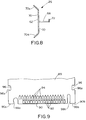
- FIG. 9 the mating end of a printed circuit board 89 having a mating edge 90 for insertion into board-receiving slot 14 of connector housing 12, is illustrated.
- the board has one row of contact pads 92 along edge 90 for engagement by contact points 54a of spring contact elements 54 of ground terminals 40.
- the board has a second row of contact pads 94 spaced inwardly of edge 90 for engagement by contact points 50a of spring contact elements 50 of signal terminals 38.
- Notches 96 can be seen formed in the side edges of the board for engagement therewithin by locking edges 66b (Fig. 7) of board-lock flanges 66 of board latches 26.
- the board also has a pair of differently sized and/or shaped polarizing notches 98a and 98b formed in edge 90 near the opposite ends thereof.
- These polarizing notches 98a and 98b embrace polarizing projections or bosses 100a and 100b, respectively, shown in Figure 5 within board-receiving slot 14.
- the polarizing notches and bosses effectively polarize the printed circuit board lengthwise of the elongated connector housing.
Landscapes
- Coupling Device And Connection With Printed Circuit (AREA)
- Details Of Connecting Devices For Male And Female Coupling (AREA)
Applications Claiming Priority (2)
| Application Number | Priority Date | Filing Date | Title |
|---|---|---|---|
| US08/555,437 US5725389A (en) | 1995-11-09 | 1995-11-09 | Edge card connector |
| US555437 | 1995-11-09 |
Publications (2)
| Publication Number | Publication Date |
|---|---|
| EP0773607A2 true EP0773607A2 (fr) | 1997-05-14 |
| EP0773607A3 EP0773607A3 (fr) | 1999-12-08 |
Family
ID=24217256
Family Applications (1)
| Application Number | Title | Priority Date | Filing Date |
|---|---|---|---|
| EP96117589A Withdrawn EP0773607A3 (fr) | 1995-11-09 | 1996-11-02 | Connecteur de bord de carte |
Country Status (6)
| Country | Link |
|---|---|
| US (1) | US5725389A (fr) |
| EP (1) | EP0773607A3 (fr) |
| JP (1) | JP2756668B2 (fr) |
| KR (1) | KR970030202A (fr) |
| SG (1) | SG66333A1 (fr) |
| TW (1) | TW390527U (fr) |
Cited By (2)
| Publication number | Priority date | Publication date | Assignee | Title |
|---|---|---|---|---|
| GB2326290A (en) * | 1997-06-13 | 1998-12-16 | Japan Aviation Electron | Edge connector for LCD display |
| SG99878A1 (en) * | 2000-02-14 | 2003-11-27 | Molex Inc | Circuit board straddle mounted connector |
Families Citing this family (11)
| Publication number | Priority date | Publication date | Assignee | Title |
|---|---|---|---|---|
| US6464537B1 (en) * | 1999-12-29 | 2002-10-15 | Berg Technology, Inc. | High speed card edge connectors |
| US6394823B1 (en) | 2000-05-26 | 2002-05-28 | Molex Incorporated | Connector with terminals having increased capacitance |
| USD472218S1 (en) | 2001-12-07 | 2003-03-25 | Hon Hai Precision Ind. Co., Ltd. | Electrical connector |
| US6790054B1 (en) | 2003-03-18 | 2004-09-14 | Sullins Electronic Corporation | Two-piece right angle contact edge card connector |
| CN100562210C (zh) * | 2006-02-22 | 2009-11-18 | 鸿富锦精密工业(深圳)有限公司 | 电路板组合 |
| JP2012142152A (ja) * | 2010-12-28 | 2012-07-26 | Tyco Electronics Japan Kk | 回路基板組立体、基板装置、回路基板組立体の組み立て方法 |
| DE102015205964A1 (de) * | 2015-02-17 | 2016-08-18 | Te Connectivity Germany Gmbh | Abgewinkelter Kontaktstift zum Einpressen in eine Kontaktstiftaufnahme, Steckverbinder mit wenigstens einem Kontaktstift und Verfahren zur Herstellung eines Steckverbinders |
| EP3278401B1 (fr) | 2015-04-01 | 2021-11-03 | TE Connectivity Germany GmbH | Broche de contact coudée destinée à être poussée dans une prise de broche de contact, connecteur pourvu d'au moins une broche de contact, et procédé de fabrication d'un connecteur |
| US9570824B1 (en) | 2015-09-23 | 2017-02-14 | Dell Products, L.P. | Reinforced right-angle type board edge connector |
| US10811794B2 (en) * | 2018-01-11 | 2020-10-20 | Te Connectivity Corporation | Card edge connector system |
| US10971863B1 (en) * | 2019-09-25 | 2021-04-06 | Greenconn Corp. | High speed connector assembly and electrical connector thereof |
Citations (2)
| Publication number | Priority date | Publication date | Assignee | Title |
|---|---|---|---|---|
| US4575172A (en) | 1984-04-06 | 1986-03-11 | Molex Incorporated | Low insertion force electrical connector with stress controlled contacts |
| US5203725A (en) | 1992-03-16 | 1993-04-20 | Molex Incorporated | Biased edge card connector |
Family Cites Families (10)
| Publication number | Priority date | Publication date | Assignee | Title |
|---|---|---|---|---|
| US4718859A (en) * | 1987-03-16 | 1988-01-12 | Molex Incorporated | Zero insertion force connector for flexible flat cable |
| US4957448A (en) * | 1989-10-17 | 1990-09-18 | Molex Incorporated | Low insertion force, low board stress electrical connector |
| US4990107A (en) * | 1989-11-17 | 1991-02-05 | Amp Incorporated | Integrated circuit module connector assembly |
| US5061200A (en) * | 1991-03-29 | 1991-10-29 | Yang Lee Su Lan | Stress-dispersed contact element of low insertion force electrical connector |
| DE9201757U1 (de) * | 1992-02-12 | 1992-04-09 | Corrado Computer Inc., Taipeh/T'ai-pei | Buchse für Leiterplatte |
| US5203714A (en) * | 1992-06-18 | 1993-04-20 | Kenny Tuan | Electrical connector for a printed circuit board |
| JP2587452Y2 (ja) * | 1993-12-14 | 1998-12-16 | ヒロセ電機株式会社 | 低挿抜力電気コネクタ |
| US5340328A (en) * | 1993-12-20 | 1994-08-23 | Roger Lee | PC board connector |
| US5514002A (en) * | 1994-04-28 | 1996-05-07 | Hon Hai Precision Ind. Co., Ltd. | Electrical connector assembly and contacts therein |
| JPH08185936A (ja) * | 1994-12-20 | 1996-07-16 | Berg Technol Inc | プリント基板用ソケット |
-
1995
- 1995-11-09 US US08/555,437 patent/US5725389A/en not_active Expired - Fee Related
-
1996
- 1996-08-26 TW TW087211824U patent/TW390527U/zh unknown
- 1996-10-11 JP JP8289150A patent/JP2756668B2/ja not_active Expired - Lifetime
- 1996-11-02 EP EP96117589A patent/EP0773607A3/fr not_active Withdrawn
- 1996-11-06 SG SG1996011054A patent/SG66333A1/en unknown
- 1996-11-08 KR KR1019960052939A patent/KR970030202A/ko not_active Abandoned
Patent Citations (2)
| Publication number | Priority date | Publication date | Assignee | Title |
|---|---|---|---|---|
| US4575172A (en) | 1984-04-06 | 1986-03-11 | Molex Incorporated | Low insertion force electrical connector with stress controlled contacts |
| US5203725A (en) | 1992-03-16 | 1993-04-20 | Molex Incorporated | Biased edge card connector |
Cited By (3)
| Publication number | Priority date | Publication date | Assignee | Title |
|---|---|---|---|---|
| GB2326290A (en) * | 1997-06-13 | 1998-12-16 | Japan Aviation Electron | Edge connector for LCD display |
| GB2326290B (en) * | 1997-06-13 | 2002-04-10 | Japan Aviation Electron | LCD panel connector for use in connection between an LCD panel and a circuit board |
| SG99878A1 (en) * | 2000-02-14 | 2003-11-27 | Molex Inc | Circuit board straddle mounted connector |
Also Published As
| Publication number | Publication date |
|---|---|
| SG66333A1 (en) | 1999-07-20 |
| EP0773607A3 (fr) | 1999-12-08 |
| KR970030202A (ko) | 1997-06-26 |
| JPH09139262A (ja) | 1997-05-27 |
| TW390527U (en) | 2000-05-11 |
| US5725389A (en) | 1998-03-10 |
| JP2756668B2 (ja) | 1998-05-25 |
Similar Documents
| Publication | Publication Date | Title |
|---|---|---|
| EP0561288B1 (fr) | Connecteur de carte enfichable avec moyens de rappel | |
| US5192228A (en) | Shielded surface mount electrical connector with integral barbed board lock | |
| US5112233A (en) | Electrical connector having contact retention means | |
| US5618187A (en) | Board mount bus bar contact | |
| US5290174A (en) | Electrical connector for a card reader | |
| EP0871261B1 (fr) | Améliorations d'un connecteur multi-broches | |
| US5297966A (en) | Mounting bracket for an electrical connector | |
| US5188535A (en) | Low profile electrical connector | |
| US5692928A (en) | Electrical connector having terminals with improved retention means | |
| US5145386A (en) | Low profile electrical connector | |
| US5725389A (en) | Edge card connector | |
| EP0232521A2 (fr) | Fiche à profil bas | |
| US5403215A (en) | Electrical connector with improved contact retention | |
| US6135785A (en) | Small pitch electrical connector having narrowed portion | |
| EP0487866B1 (fr) | Dispositif connecteur électrique pour assemblage sur plaquette de circuits imprimés | |
| US5292265A (en) | Edge mounted circuit board electrical connector | |
| EP0722205A2 (fr) | Assemblage de connecteur électrique pour interconnecter un câble plat à une carte de circuit imprimé | |
| US5921808A (en) | Ribbon cable plug-in connector | |
| US4148537A (en) | Zero insertion force connector for printed circuit boards | |
| US5597320A (en) | Zero insertion force electrical connector and terminal | |
| EP0488349A2 (fr) | Connecteur avec une plaque d'écartement pour des contacts ayant des voies coniques | |
| US5807142A (en) | Electrical connector having terminals with improved retention means | |
| EP0168922A2 (fr) | Connecteur à force d'insertion nulle | |
| EP0601703B1 (fr) | Support pour le montage d'un connecteur électrique | |
| EP0590958B1 (fr) | Connecteur électrique |
Legal Events
| Date | Code | Title | Description |
|---|---|---|---|
| PUAI | Public reference made under article 153(3) epc to a published international application that has entered the european phase |
Free format text: ORIGINAL CODE: 0009012 |
|
| AK | Designated contracting states |
Kind code of ref document: A2 Designated state(s): DE FR GB IT |
|
| PUAL | Search report despatched |
Free format text: ORIGINAL CODE: 0009013 |
|
| AK | Designated contracting states |
Kind code of ref document: A3 Designated state(s): DE FR GB IT |
|
| 17P | Request for examination filed |
Effective date: 20000602 |
|
| 17Q | First examination report despatched |
Effective date: 20010201 |
|
| STAA | Information on the status of an ep patent application or granted ep patent |
Free format text: STATUS: THE APPLICATION IS DEEMED TO BE WITHDRAWN |
|
| 18D | Application deemed to be withdrawn |
Effective date: 20010601 |