EP0773622A2 - Circuit d'alimentation interne - Google Patents
Circuit d'alimentation interne Download PDFInfo
- Publication number
- EP0773622A2 EP0773622A2 EP96402383A EP96402383A EP0773622A2 EP 0773622 A2 EP0773622 A2 EP 0773622A2 EP 96402383 A EP96402383 A EP 96402383A EP 96402383 A EP96402383 A EP 96402383A EP 0773622 A2 EP0773622 A2 EP 0773622A2
- Authority
- EP
- European Patent Office
- Prior art keywords
- power supply
- node
- switching means
- supply terminal
- terminal
- Prior art date
- Legal status (The legal status is an assumption and is not a legal conclusion. Google has not performed a legal analysis and makes no representation as to the accuracy of the status listed.)
- Withdrawn
Links
Images


Classifications
-
- H—ELECTRICITY
- H02—GENERATION; CONVERSION OR DISTRIBUTION OF ELECTRIC POWER
- H02M—APPARATUS FOR CONVERSION BETWEEN AC AND AC, BETWEEN AC AND DC, OR BETWEEN DC AND DC, AND FOR USE WITH MAINS OR SIMILAR POWER SUPPLY SYSTEMS; CONVERSION OF DC OR AC INPUT POWER INTO SURGE OUTPUT POWER; CONTROL OR REGULATION THEREOF
- H02M3/00—Conversion of DC power input into DC power output
- H02M3/02—Conversion of DC power input into DC power output without intermediate conversion into AC
- H02M3/04—Conversion of DC power input into DC power output without intermediate conversion into AC by static converters
- H02M3/06—Conversion of DC power input into DC power output without intermediate conversion into AC by static converters using resistors or capacitors, e.g. potential divider
- H02M3/07—Conversion of DC power input into DC power output without intermediate conversion into AC by static converters using resistors or capacitors, e.g. potential divider using capacitors charged and discharged alternately by semiconductor devices with control electrode, e.g. charge pumps
Definitions
- the present invention relates to a power supply circuit, more particularly to a booster circuit generating a voltage higher than an external power supply voltage by raising the voltage from the external power supply voltage, or to a down converter or other DC (direct current)-DC converter generating a voltage lower than the external power supply voltage by lowering the voltage from the external power supply voltage.
- the external power supply used is usually a 5V single power supply, but it has become necessary to operate semiconductor devices at a lower internal voltage due to the desire to deal with the deterioration of the voltage resistance of semiconductor devices accompanying higher integration and the desire to reduce power consumption.
- An object of the present invention is to provide a power supply circuit able to decrease the number of charge pumping circuits used for obtaining a desired high voltage by increasing the efficiency of raising or lowering the voltage and to give a stable output voltage with a low power loss.
- an internal power supply circuit comprising a plurality of charge accumulating means, a first power supply terminal, a second power supply terminal, a first switching means for connecting the plurality of charge accumulating means in parallel to each other in a first state, and a second switching means for connecting the plurality of charge accumulating means in series with each other in a second state, and a control means for energizing the first switching means or the second switching means in response to the first state or the second state to connect the plurality of charge accumulating means between the first power supply terminal and the second power supply terminal, and for deenergizing the first switching means or the second switching means in response to the first state or the second state to disconnect the plurality of charge accumulating means between the first power supply terminal and the second power supply terminal, the control means repeating the energizing and the deenergizing.
- the charge accumulating means are constituted by capacitors; the first switching means is constituted by a third switching means and a fourth switching means; and a partial booster circuit is comprised by a capacitor connected between a first node and a second node, the third switching means connected between the first node and the first power supply terminal, and the fourth switching means connected between the second node and the second power supply terminal; a plurality of the partial booster circuits is provided; the second switching means holds in a non-conductive state the first node of a front partial booster circuit and the second node of a rear partial booster circuit in the first state and holds them in a conductive state in the second state; the first switching means comprised of the third switching means and the fourth switching means being held in the conductive state and the second switching means being held in a non-conductive state in the first state; and the first switching means comprised of the third switching means and the fourth switching means being held in the non-conductive state and the second switching means being held in a conductive state in the second state so as to raise the voltage
- the internal power supply circuit of the present invention further comprises a biasing means connected to the second node of the initial stage partial booster circuit for holding the second node at a constant potential and a rectifying means connected between the first node of the final stage partial booster circuit and a boosted voltage output terminal.
- the biasing means is constituted by a switching means set in the conductive state when the first switching means comprised of the third and fourth switching means is non-conductive.
- the first power supply terminal is a positive power supply terminal and the second power supply terminal is a negative power supply terminal
- the constant potential is the potential of the first power supply terminal
- the biasing means is a rectification element connected so that a direction from the first power supply toward the second node of the initial stage partial booster circuit becomes a forward direction
- the rectification element is connected so that a direction from the first node of the final stage partial booster circuit toward the output terminal becomes the forward direction and supplies the positive boosted voltage to the output terminal.
- the first power supply terminal is a negative power supply terminal and the second power supply terminal is a positive power supply terminal
- the constant potential is the potential of the second power supply terminal
- the biasing means is a rectification element connected so that a direction from the second node of the first stage partial booster circuit toward the first power supply terminal becomes the forward direction
- the rectification element is connected so that a direction from the output terminal to the first node of the final stage partial booster circuit becomes the forward direction and supplies the negative boosted voltage to the output terminal.
- the third switching means is constituted by a first conductivity type insulation gate type field effect transistor with a gate electrode connected to an input terminal of a first clock, with one diffusion layer connected to the first power supply, and with another diffusion layer connected to the first node of the partial booster circuit;
- the fourth switching means is constituted by a first conductivity type insulation gate type field effect transistor with a gate electrode connected to an input terminal of a second clock, with one diffusion layer connected to the second power supply, and with another diffusion layer connected to the second node of the partial booster circuit;
- the second switching means is constituted by a second conductivity type insulation gate type field effect transistor with a gate electrode connected to the input terminal of a third clock.
- the biasing means is constituted by a second conductivity type insulation gate type field effect transistor with a gate electrode connected to the input terminal of a third clock.
- an amplitude of the first clock is set larger than a potential difference between the first power supply terminal and the second power supply terminal.
- the first power supply terminal is a positive power supply terminal and the first conductivity type insulation gate type field effect transistor is an n-channel type transistor and is held at a higher level than the first power supply terminal voltage in a high level section of the first clock.
- the first power supply is a negative power supply terminal and the first conductivity type insulation gate type field effect transistor is a p-channel type transistor and is held at a lower level than the second power supply terminal voltage in a low level section of the first clock.
- the second conductivity type insulation gate type field effect transistor constituting the second switching means is formed in an independent well.
- the biasing means is a second conductivity type insulation gate type field effect transistor formed in the same well as that for the second conductivity type insulator gate type field effect transistors constituting part of the peripheral logic circuit.
- an internal power supply circuit comprising a first power supply terminal, a second power supply terminal, a first node, a second node, a capacitor connected between the first node and the second node, a first switching means connected between the first node and the first power supply terminal, a second switching means connected between the second node and the second power supply terminal, a biasing means connected to the second node and biasing the node at a constant potential, and a rectifying means connected between the first node and the boosted voltage output terminal, the first and second switching means being repeatedly set in the conductive state and the non-conductive state to be overlapped thereby to output a boosted voltage to an output terminal.
- the biasing means is a rectification element connected so that a direction from the first power supply toward the second node becomes a forward direction, and the rectifying means is connected so that a direction from the first node toward the boosted voltage output terminal becomes the forward direction.
- the biasing means is a rectification element connected so that a direction from the second node toward the first power supply becomes a forward direction
- the rectifying means is connected so that a direction from the boosted voltage output terminal toward the first node becomes the forward direction.
- the charge accumulating means are constituted by capacitors; the capacitors are connected in series between the first and second power supply terminals and then are charged in the second state; and the capacitors are connected in parallel between the second power supply terminal and a down voltage output terminal in the first state to thereby obtain a voltage between the first and second power supply terminal.
- a switching means connecting to an external power supply between the voltage of the first power supply terminal and the voltage of the second power supply terminal, having at least one sub-power supply of a potential lower than the external power supply, and operationally connects the external power supply and the sub-power supply, and a means for sequentially switching the connection and nonconnection state from the switching means connected to the external power supply to cause charging and discharging of the capacitors.
- At least two arrangements of a plurality of capacitors which are switched between the serial connection and parallel connection based on a clock signal,and clock signals having inverse phases are supplied to the above at least two arrangements.
- the capacitors are composed of ferroelectric capacitors, high dielectric capacitors, MIM (metal-insulator-metal) configuration capacitors, DRAM trench and stack capacitors, planar capacitors, external capacitors, or MIS (metal-insulator-semiconductor) gate capacitors.
- MIM metal-insulator-metal
- DRAM trench and stack capacitors planar capacitors
- MIS metal-insulator-semiconductor
- the capacitance element of each booster stage is charged to the differential voltage level between the first power supply and the second power supply, then the first and second switching means are changed over to the nonconductive state and the third switching means is changed over to the conductive state, whereby the charged capacitance elements are connected in series between the constant potential and the output terminal of the power supply circuit and a positive or negative boosted voltage is output to the output terminal of the power supply circuit.
- the loss of the boosted voltage becomes only the voltage drop of the rectification element connected between the final stage and the output terminal, the reduction of the boosting efficiency accompanying the rise of the threshold voltage due to the substrate biasing effect can be avoided, and a reduction of the number of booster stages needed for obtaining a desired high voltage and a shortening of the rising time of the boosted voltage can be achieved.
- the value of the external power supply voltage is detected by a detecting circuit and the number of connections of the plurality of capacitance elements is switched in accordance with this detected voltage.
- the number of the capacitance elements set in accordance with the detected voltage are connected in series between the external power supply and the reference power supply and next connected in parallel and, at the same time, the connection and nonconnection states sequentially switched from the switching means connected to the external power supply to perform charging and discharging, thus an output voltage of a value between the external power supply voltage and the reference power supply voltage is obtained.
- the switching between the serial connection and parallel connection of the capacitance elements is carried out based on the clock signal. Further, two systems of the plurality of capacitance elements are respectively driven by clock signals having inverse phases to each other. By this, the ripple accompanying the load current can be lowered.
- the capacitance element is comprised by an element having a high relative dielectric constant such as a ferroelectric capacitance, whereby the power loss is reduced.
- Figure 1 is a circuit diagram of a representative example of a conventional power supply circuit constituted by a booster circuit.
- M1 to M4 are n-channel type MOS transistors, and C L is a load capacitor.
- the power supply circuit of Fig. 1 is constituted by connecting a plurality of stages of partial circuits (booster stages) each comprising one capacitor, for example, C2, and one nMOS transistor, for example, M2, in series.
- One of the electrodes of each of the capacitors C2, C3, C4 constituting a booster stage is connected to a common connecting point of the gate electrodes and drain diffusion layers of the nMOS transistors M2, M3, M4.
- the other electrodes of the capacitors C2, C3, C4 are alternately connected to respective ones of the supply lines of clocks 0 ⁇ 1 and 0 ⁇ 2.
- the common connecting point of the gate electrodes and drain diffusion layers of the diode-connected n-channel type MOS transistors constituting the booster stages is connected to the source diffusion layer of the n-channel type MOS transistor of the booster stage of the preceding stage, while the source diffusion layer is connected to the common connecting point of the gate electrodes and the drain diffusion layers of the diode-connected n-channel type MOS transistors of the next stage.
- the order of connection of the clocks 0 ⁇ 1 and 0 ⁇ 2 is one where the odd number booster stages are connected to the clock 0 ⁇ 1 and the even number stages are connected to the clock 0 ⁇ 2.
- the above power supply circuit constituted in this way attracts the charges from a semiconductor substrate on which a power supply voltage V CC and the present circuit are formed by supplying the clocks ⁇ 1 and ⁇ 2 with inverse phases and supplies a boosted voltage V OUT to an output terminal T OUT .
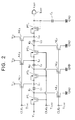
- Figure 2 is a circuit diagram of a first embodiment of the power supply circuit according to the present invention.
- CLK 1 , CLK 2 , and CLK 3 denote clock signals
- T CLK1 , T CLK2 , and T CLK3 denote clock signal input terminals
- PT 1 denotes a p-channel type (pMOS) transistor serving as a biasing means
- PT 2 and PT 3 denote pMOS transistors serving as the third switching means
- PT L denotes diode-connected pMOS transistor
- NU 1 , NU 2 , and NU 3 denote n-channel MOS (nMOS) transistors serving as the first switching means
- NL 1 , NL 2 , and NL 3 denote nMOS transistors serving as the second switching means
- K 1 , K 2 , K 3 , L 1 , L 2 , and L 3 denote nodes of the booster stages
- C 1 , C 2 , and C 3 denote capacitance elements (capacitors) for boosting
- C L denotes a parasitic capacitance of the load
- the power supply circuit shown in Fig. 2 is constituted by the booster stages shown in Fig. 3.
- the booster stage shown in Fig. 3 is a booster stage of the i-th stage.
- the booster stage of i-th stage is constituted by a capacitor C i , nodes K i and L i , and nMOS transistors NU i and NL i .
- the capacitor C i is connected between the node K i and the node L i .
- the gate electrode of the nMOS transistor NU i is connected to the input terminal of the clock signal CLK 1 , one diffusion layer is connected to the supply line of the power supply voltage V CC , and the other diffusion layer is connected to the node L i .
- the gate electrode of the nMOS transistor NL i is connected to the input terminal of the clock signal CLK 2 , one diffusion layer is connected to the node K i , and the other diffusion layer is connected to the ground line.
- the power supply circuit shown in Fig. 2 is configured with three stages of the booster stages shown in Fig. 3 connected in series.
- the node K 1 of the first booster stage is connected via the pMOS transistor PT 1 to the supply line of the power supply voltage V CC .
- the source electrode of the pMOS transistor PT 1 is connected to the supply line of the power supply voltage V CC
- the drain electrode is connected to the node K 1 .
- the gate electrode of the pMOS transistor PT 1 is connected to the input terminal T CLK3 of the clock signal CLK 3 .
- the node L 1 of the booster stage of the first stage is connected via the pMOS transistor PT 2 to the node K 2 of the second booster stage.
- the source electrode of the pMOS transistor PT 2 is connected to the node L 1 of the first booster stage, and the drain electrode is connected to the node K 2 of the second booster stage.
- the gate electrode of the pMOS transistor PT 2 is connected to the input terminal T CLK3 of the clock signal CLK 3 .
- the node L 2 of the second booster stage is connected via the pMOS transistor PT 3 to the node K 3 of the third booster stage.
- the source electrode of the pMOS transistor PT 3 is connected to the node L 2 of the second booster stage, and the drain electrode is connected to the node K 3 of the third booster stage.
- the gate electrode of the pMOS transistor PT 3 is connected to the input terminal T CLK3 of the clock signal CLK 3 .
- the node L 3 of the third booster stage is connected via the pMOS transistor PT L to the output terminal T OUT of the power supply circuit.
- the source electrode of the pMOS transistor PT L is connected to the node L 3 of the third booster stage, and the drain electrode is connected to the output terminal T OUT of the power supply circuit.
- the gate electrode of the pMOS transistor PT L is connected to the output terminal T OUT commonly with the drain electrode. Namely, the pMOS transistors PT L are diode-connected.
- the output terminal T OUT is grounded via the load capacitor C L .
- the pMOS transistor PT 1 serving as the biasing means is for example formed in the same well as that of the other transistors constituting the peripheral circuits of the power supply circuit.
- pMOS transistors PT 2 and PT 3 are formed in each independent well as the third switching means.
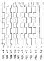
- a clock signal CLK 1 is supplied to the gate electrodes of the nMOS transistors NU 1 , NU 2 , and NU 3 constituting the booster stages.
- the high level of the clock signal CLK 1 is held at a higher level than the power supply voltage V CC , for example, a potential of (V CC + V TN ).
- V TN is a threshold voltage of the nMOS transistors NU 1 , NU 2 , and NU 3 .
- a voltage higher than the power supply voltage V CC for example, a voltage of (V CC + V TN ) is supplied to the gate electrodes of the nMOS transistors NU 1 , NU 2 , and NU 3 constituting the booster stages.
- the drain electrodes of these transistors are held at a potential of the same level as that of the power supply voltage V CC .
- the clock signal CLK 2 supplied to the gate electrodes of the nMOS transistors NL 1 , NL 2 , and NL 3 constituting the booster stages is held at a high level and low level in synchronization with the clock signal CLK 1 .
- the high level of the clock signal CLK 2 is held at for example the power supply voltage V CC level.
- the clock signal CLK 1 and the clock signal CLK 2 are held at a high level, and the capacitors C 1 , C 2 and C 3 existing in the booster stages are charged to for example the power supply voltage V CC level.
- both of the clock signal CLK 1 and clock signal CLK 2 are switched to the low level, therefore the nMOS transistors NU 1 , NU 2 , and NU 3 and NL 1 , NL 2 , and NL 3 constituting the booster stages are set in the nonconductive state at the time t 2 .
- the clock signal CLK 3 is switched from the high level to the low level, for example, the ground potential GND.
- the pMOS transistors PT 1 , PT 2 , and PT 3 are switched to the conductive state.
- the capacitors C 1 , C 2 , and C 3 all charged to the power supply voltages V CC level are connected in series between the node K 1 of the first stage and the output terminal T OUT of the power supply circuit, and a voltage obtained by multiplying the power supply voltage by (number of booster stages + 1) is obtained at one end of the capacitor of the final stage.
- the threshold voltage of the pMOS transistors PT L diode-connected between the node L n of the booster stage of the final stage and the output terminal T OUT is defined as V TP
- the boosted voltage V OUT obtained by the power supply circuit V OUT (n+1) x V CC - V TP
- the node K 1 of the booster stage of the first stage is held at the power supply voltage V CC level, and the node L 1 is held at the 2V CC level.
- the node K 2 of the second stage is held at 2V CC in the same way as the node L 1 of the first stage, and the node L 2 of the second stage is held at 3V CC .
- the node K 3 of the third stage is held at 3V CC in the same way as the node L 2 of the second stage, and the node L 3 of the third stage is held at 4V CC .
- the pMOS transistors PT L are diode-connected. The connection is made so that the direction from the node L 3 of the third stage toward the output terminal T OUT becomes the forward direction, therefore the voltage of the node L 3 is output to the output terminal T OUT . By this, the capacitor C L is charged, and a boosted voltage V OUT of substantially 4V CC is output to the output terminal T OUT .
- Figure 5 is a circuit diagram of a clock generating circuit showing an example of the circuit for generating the clock signals CLK 1 , CLK 2 , and CLK 3 shown in Fig. 2.
- the clock generating circuit of the present example is constituted by RS flip-flops RFF 1 , RFF 2 , RFF 3 , RFF 4 , RFF 5 , and RFF 6 , a clock generator 10, and delay circuits DLY 1 and DLY 2 .
- FIG. 6 An example of the configuration of the clock generator 10 is shown in Fig. 6.
- the clock generator 10 is constituted by the nMOS transistors NA, NB, NC, and ND and a capacitor C CK .
- One diffusion layer of the nMOS transistor NB is connected to the supply line of the power supply voltage V CC , the other diffusion layer is connected to the node ND 1 , and the gate electrode is connected to the input terminal of the clock signal B .
- One diffusion layer of the nMOS transistor NA is connected to the node ND 1 , the other diffusion layer is grounded, and the gate electrode is connected to the input terminal of the clock signal A .
- One diffusion layer of the nMOS transistor ND is connected to the supply line of the power supply voltage V CC , the other diffusion layer is connected to the node ND 2 , and the gate electrode is connected to the input terminal of the clock signal D .
- One diffusion layer of the nMOS transistor NC is connected to the node ND 2 , the other diffusion layer is grounded, and the gate electrode is connected to the input terminal of the clock signal C .
- a capacitor C CK is connected between the node ND 1 and the node ND 2 , and the node ND 2 is connected to the output terminal T 1 of the clock signal CLK 1 .
- the clock signals A , B , C , and D shown in Figs. 7A to 7D are input to the clock generator 10.
- the clock generator 10 Upon receipt of this, the clock generator 10 generates a clock signal CLK 1 held at a higher level than that of the power supply voltage V CC at the time of a high level.
- the set signal input terminal S of the RS flip-flop RFF 1 is connected to the inverted output terminal of the RS flip-flop RFF 5
- a reset signal input terminal R is connected to the inverted output terminal of the RS flip-flop RFF 2 .
- the output terminal of the RS flip-flop RFF 1 is connected to the set signal input terminal S of the RS flip-flop RFF 2 , and the inverted output terminal is connected to the reset signal input terminal R of the RS flip-flop RFF 6 .
- the inverted output signal of the RS flip-flop RFF 1 is output as the clock signal C to the clock generator 10.
- the reset signal input terminal R of the RS flip-flop RFF 2 is connected to the inverted output terminal of the RS flip-flop RFF 3 , and the output terminal is connected to the set signal input terminal S of the RS flip-flop RFF 3 .
- the output signal of the RS flip-flop RFF 2 is supplied to the clock generator 10 as the clock signal D .
- the reset signal input terminal R of the RS flip-flop RFF 3 is connected to the inverted output terminal of the RS flip-flop RFF 4 , and the output terminal is connected to the set signal input terminal S of the RS flip-flop RFF 4 .
- the inverted output signal of the RS flip-flop RFF 3 is supplied to the clock generator 10 as the clock signal A .
- the reset signal input terminal R of the RS flip-flop RFF 4 is connected to the inverted output terminal of the RS flip-flop RFF 5 , and the output terminal is connected to the set signal input terminal S of the RS flip-flop RFF 5 via the delay circuit DLY 1 .
- the output signal of the RS flip-flop RFF 4 is supplied to the clock generator 10 as the clock signal B .
- the reset signal input terminal R of the RS flip-flop RFF 5 is connected to the output terminal of the RS flip-flop RFF 6 , and the inverted output terminal is connected to the output terminal T 2 of the clock signal CLK 2 .
- the reset signal input terminal R of the RS flip-flop RFF 6 is connected to the inverted output terminal of the RS flip-flop RFF 1 , the set signal input terminal S is connected to the output terminal of the delay circuit DLY 2 , and the input terminal of the delay circuit DLY 2 is connected to the inverted output terminal of the RS flip-flop RFF 6 .
- the output terminal of the RS flip-flop RFF 6 is connected to the output terminal T 3 of the clock signal CLK 3 .
- the clock generating circuit shown in Fig. 5 generates the clock signals A , B , C , and D shown in Figs. 7A to 7H and the clock signals CLK 1 , CLK 2 , and CLK 3 .
- the clock signals A , B , C , and D are clock signals alternately taking a high level, for example, the power supply voltage V CC level, and a low level, for example, the ground potential GND level.
- the clock signals CLK 2 and CLK 3 are clock signals alternately taking a high level, for example, the power supply voltage V CC level, and a low level, for example, the ground potential GND level.
- the clock signals A , B , C , and D are input to the clock generator 10.
- the clock generator 10 generates a clock signal CLK 1 which is held at a level of more than the power supply voltage V CC at the time of the high level and is held at for example the ground potential GND level at the time of the low level.
- the node ND 1 is held at the ground potential GND level, and the node ND 2 side is held at a voltage reduced from the power supply voltage V CC by exactly the threshold voltage V TN of the nMOS transistor ND, therefore the capacitor C CK is charged to (V CC - V TN ).
- the clock signal B is switched from the low level to the high level. Also, at this time, both of the clock A and clock C are held at the low level, and the nMOS transistors NA and NC are set in the nonconductive state.
- the nMOS transistor NB is switched to the conductive state, and the node ND 1 is held at a voltage reduced from the power supply voltage V CC by exactly the threshold voltage V TN of the nMOS transistor NB, that is, (V CC - V TN ).
- the node ND 2 is held at 2(V CC - V TN ).
- the voltage of the output terminal T 1 of the clock signal CLK 1 rises by one stage and becomes 2(V CC - V TN ), that is, is held at a higher level than that of the power supply voltage V CC .
- the clock signal B is switched from the high level to the low level, and the clock signal A is switched from the low level to the high level in accordance with this. Further, in accordance with this, the clock signal C is switched to the high level, and the clock signal D is switched to the low level.
- the potentials of the nodes ND 1 and ND 2 are switched to the ground potential, and the output terminal T 1 of the clock signal CLK 1 is held at the ground potential. Then, at the time t 2 , the clock signal CLK 3 is switched from the high level to the low level.
- the clock signal CLK 2 and the clock signal CLK 3 are switched from the low level to the high level.
- the clock signal C is switched to the low level and the clock signal D is switched to the high level, therefore, the capacitor C CK is charged to (V CC - V TN ) again.
- the clock generating circuit shown in Fig. 5 generates the clock signal CLK 1 which is held at 2(V CC - V TN ) level at the time of the high level and held at the ground potential at the time of the low level and the clock signal CLK 2 and the clock signal CLK 3 which are held at the power supply voltage V CC level at the time of the high level and held at the ground potential at the time of the low level and supplies them to the power supply circuit shown in Fig. 2.
- the clock signal CLK 1 held at a higher level than the power supply voltage V CC at the time of the high level is supplied to the gate electrodes of the nMOS transistors NU 1 , NU 2 , and NU 3 constituting the booster stages
- the clock signal CLK 2 is supplied to the gate electrodes of the nMOS transistors NL 1 , NL 2 , and NL 3
- the clock signal CLK 3 is supplied to the gate electrodes of the pMOS transistors PT 1 , PT 2 , and PT 3 connected between the booster stages
- the clock signals CLK 1 and CLK 3 are held at the high level
- the capacitors C 1 , C 2 , and C 3 of the booster stages are charged to the power supply voltage V CC level
- the clock signals CLK 1 and CLK 2 are switched to the low level
- the clock signal CLK 3 is switched to the high level
- the boosted voltage V OUT is supplied to the output terminal T OUT of the power supply circuit, therefore there is no loss of
- Figure 8 is a circuit diagram of a second embodiment of the power supply circuit according to the present invention.
- Fig. 8 is a circuit diagram of the power supply circuit showing an example of the negative booster circuit for generating a negative boosted voltage compared with the power supply voltage V CC .
- the power supply circuit can be used for biasing for example a structure of a semiconductor circuit such as a dynamic random access memory.
- CLK B2 and CLK B3 are inverted signals of the clock signals CLK 2 and CLK 3 shown in Fig. 1, and CLK B1 is a clock signal which is held at the power supply voltage V CC level at the time of the high level in synchronization with the clock signal CLK B2 and held at a level lower than the ground potential GND, that is, a negative potential at the time of the low level.
- T CLKB1 , T CLKB2 , and T CLKB3 denote input terminals of the clock signals CLK B1 , CLK B2 , and CLK B3
- NT 1 denotes an nMOS transistor serving as the biasing means
- NT 2 and NT 3 denote nMOS transistors serving as the third switching means
- NT L denotes diode-connected nMOS transistor
- PL 1 , PL 2 , and PL 3 denote pMOS transistors serving as the first switching means
- PU 1 , PU 2 , and PU 3 denote pMOS transistors serving as the second switching means
- KB 1 , KB 2 , KB 3 , LB 1 , LB 2 , and LB 3 denote nodes of booster stages
- C 1 , C 2 , and C 3 denote capacitors for boosting
- C L denotes a parasitic capacitance of the load
- T OUTB denotes an output terminal of the negative
- the power supply circuit of the present example was constituted by three booster stages constituted by pMOS transistors PU 1 , PU 2 , PU 3 , PL 1 , PL 2 , and PL 3 and capacitors C 1 , C 2 , and C 3 .
- the gate electrode of the pMOS transistor PU i is connected to the input terminal of the clock signal CLK B2 , the source electrode is connected to the supply line of the power supply voltage V CC , and the drain electrode is connected to the node KB i of the booster stage.
- the gate electrode of the pMOS transistor PL i is connected to the input terminal of the clock signal CLK B1 , the source electrode is connected to the node LB i , and the drain electrode is grounded.
- One electrode of the capacitor C i is connected to the node KB i , and the other electrode is connected to the node LB i .
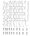
- Figure 10A to 10J are waveform diagrams of the clock signals CLK B1 , CLK B2 , and CLK B3 , the voltages of the boosting nodes KB 1 , LB 1 , KB 2 , LB 2 , KB 3 , and LB 3 , and the output voltage V OUTB .
- the clock signal CLK B1 and the clock signal CLK B2 are synchronous.
- the clock signal CLK B1 is held at the power supply voltage V CC level at the time of the high level and is held at the level lower than the ground potential GND, that is, a negative potential, at the time of the low level.
- the clock signal CLK B2 is held at the power supply voltage V CC level at the time of the high level and is held at the ground potential GND level at the time of the low level.
- the clock signals CLK B1 and CLK B2 are switched from the high level to the low level.
- the clock signal CLK B1 is held at the negative potential and the clock signal CLK B2 is held at the ground potential GND level.
- the pMOS transistors PU 1 , PU 2 , and PU 3 and the pMOS transistors PL 1 , PL 2 , and PL 3 are held in the conductive state, and the capacitors C 1 , C 2 , and C 3 are charged.
- the nodes LB 1 , LB 2 , and LB 3 are held at the ground potential GND level, the nodes KB 1 , KB 2 , and KB 3 are held at the power supply voltage V CC level, and the capacitors C 1 , C 2 , and C 3 are charged to the power supply voltage V CC level.
- the clock signals CLK B1 and CLK B2 are switched from the low level to the high level, and the pMOS transistors PU 1 , PU 2 , and PU 3 and the pMOS transistors PL 1 , PL 2 , and PL 3 are switched to the nonconductive state.
- the clock signal CLK B3 is switched from the low level to the high level, and the nMOS transistors NT 1 , NT 2 , and NT 3 are switched to the conductive state in accordance with this.
- the node KB 1 is held at the ground potential GND level, and the node LB 1 is held at the -V CC level.
- the node KB 2 is held at the -V CC level in the same way as the node LB 1 , and the node LB 2 is held at the -2V CC level.
- the node KB 3 is held at the -2V CC level in the same way as the node LB 2 , and the node LB 3 is held at the -3V CC level.
- the potential of the node LB 3 is output to the output terminal T OUTB via the diode-connected nMOS transistors NT L .
- the threshold voltage of the nMOS transistor NT L as V TN
- the negative boosted voltage V OUTB output to the output terminal T OUTB becomes -(3V CC - V TN ).
- V OUTB -(n x V CC - V TN )
- the voltage loss of the boosted voltage V OUTB obtained by the negative booster circuit shown in Fig. 8 is only the voltage drop in the diode-connected between the final stage and the output terminal T OUTB , and an improvement of the efficiency of the power supply circuit can be achieved.
- the nMOS transistor NT 1 is formed in the same well as that for the other transistors constituting the peripheral circuit of for example the negative booster circuit, and nMOS transistors NT 2 and NT 3 are formed in the individually independent wells.
- Figure 11 is a circuit diagram of an example of the generator 10a of the clock signal CLK B1 in the second embodiment.
- the clock generator 10a is constituted by the nMOS transistors NA B , NB B , NC B , and ND B and the capacitor C CK .
- One diffusion layer of the nMOS transistor NB B is connected to the supply line of the power supply voltage V CC , the other diffusion layer is connected to the node ND 1 , and the gate electrode is connected to the input terminal of the clock signal B B .
- One diffusion layer of the nMOS transistor NA B is connected to the node ND 1 , the other diffusion layer is grounded, and the gate electrode is connected to the input terminal of the clock signal A B .
- One diffusion layer of the nMOS transistor ND B is connected to the supply line of the power supply voltage V CC , the other diffusion layer is connected to the node ND 2 , and the gate electrode is connected to the input terminal of the clock signal D B .
- One diffusion layer of the nMOS transistor NC B is connected to the node ND 2 , the other diffusion layer is grounded, and the gate electrode is connected to the input terminal of the clock signal C B .
- a capacitor C CK is connected between the node ND 1 and the node ND 2 , and the node ND 2 is connected to the output terminal T B1 of the clock signal CLK B1 .
- the clock signals A B , B B , C B , and D B shown in Figs. 12A to 12D are input to the clock generator 10a.
- the clock generator 10a Upon receipt of these clock signals, the clock generator 10a generates a clock signal CLK B1 which is held at the power supply voltage V CC at the time of the high level and is held at a lower level than the ground potential GND at the time of the low level.
- the clock signals B B and C B are switched to the high level, for example, the power supply voltage V CC level. Note that, at this time, both of the clock signals A B and D B are held at the low level, for example, the ground potential GND.
- the nMOS transistors NA B and ND B are set in the nonconductive state, and both of the nMOS transistors NB B and NC B are set in the conductive state.
- the capacitor C CK is charged, and the node ND 1 is held at a voltage which becomes lower than the power supply voltage V CC by exactly the threshold voltage V TN of the nMOS transistor NB B , that is, (V CC - V TN ).
- the clock signals B B and C B are switched to the low level, and the clock signal A B is raised to the high level, for example, the power supply voltage V CC level. Note that, at this time, the clock signal D B is held at the low level as it is.
- both of the nMOS transistors NB B and NC B are switched to the nonconductive state, and the nMOS transistor NA B is switched to the conductive state. Further, the nMOS transistor ND B is held in the nonconductive state as it is. For this reason, the node ND 1 is held at the ground potential GND, and the node ND 2 is held at the negative potential, for example -(V CC - V TN ).
- the clock signal A B is switched to the low level, and the clock signal D B is raised to the high level, for example, the power supply voltage V CC .
- the nMOS transistor NA B is switched to the nonconductive state, and the nMOS transistor ND B is switched to the conductive state.
- the clock signals B B and C B are held at the low level, and both of the nMOS transistors NB B and NC B are held in the nonconductive state, therefore the node ND 2 is held at the power supply voltage V CC level.
- the clock signal D B is switched to the low level, and both of the clock signals B B and C B are raised to the high level, therefore both of the nMOS transistors NB B and NC B are set in the conductive state, and the capacitor C CK is charged and the node ND 1 is held at the (V CC - V TN ) level.
- the clock generator 10a shown in Fig. 11 generates a clock signal CLK B1 which is held at a level lower than the ground potential GND during the low level section and is held at the power supply voltage V CC level in the high level section and outputs the same from the output terminal T B1 . Then, this clock signal CLK B1 is supplied to the negative booster circuit shown in Fig. 8, and the negative boosted voltage V OUTB is generated.
- the clock signal CLK B2 is applied to the gate electrodes of the pMOS transistors PU 1 , PU 2 , and PU 3 constituting the booster stages, the clock signal CLK B1 which is held at the power supply voltage V CC level at the time of the high level and is held at the negative potential at the time of the low level is supplied to the gate electrodes of the pMOS transistors PL 1 , PL 2 , and PL 3 , the clock signal CLK B3 is supplied to the gate electrodes of the nMOS transistors NT 1 , NT 2 , and NT 3 connected between the booster stages, the clock signals CLK B1 and CLK B2 are held at the low level, and the capacitors C 1 , C 2 , and C 3 of the booster stages are charged to the power supply voltage V CC level, then the clock signals CLK B1 and CLK B2 are switched to the high level, the clock signal CLK B3 is switched to the high level, and the negative boosted voltage
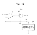
- a series regulator as shown in Fig. 13 is generally used.
- This series regulator is constituted by, as shown in Fig. 13, an operational amplifier 11 with an inverting input (-) connected to the supply line of a constant voltage V L , and a pMOS transistor 12 with a gate connected to the output of the operational amplifier 11, with a source connected to the supply line of the power supply voltage V cc , and with a drain connected to a noninverting input (+) of the operational amplifier 11 and supplies a low voltage V L from a node N 1 to a circuit block 13.
- V cc use external power supply
- the fluctuation of the V cc is large and there arises a problem of the power loss thereof.
- Figure 14 is a circuit diagram of an example of the configuration of this DC-DC converter.
- this DC-DC converter 20 is constituted by switch circuits 21 to 23 and capacitors 31 to 33.
- the switch circuits 21 to 23 are constituted by for example MOS type transistors.
- the capacitors 31 and 32 those having the same capacitance are used.
- An operational contact a of the switch circuit 21 is connected to the supply line of the power supply voltage V cc , an operational contact b is connected to an output node ND OUT , and a fixed contact c is connected to one electrode of the capacitor 31.
- the operational contact a of the switch circuit 22 is connected to the operational contact a of the switch circuit 23, the operational contact b is grounded, and the fixed contact c is connected to the other electrode of the capacitor 31.
- the operational contact b of the switch circuit 23 is connected to the output node ND OUT , and the fixed contact c is connected to one electrode of the capacitor 32. Then, the other electrode of the capacitor 32 is grounded.
- the capacitor 33 is a stabilizing capacitor which is connected between the output node ND OUT and the ground line for suppressing the voltage drop of the output node ND OUT by a load current I L and stabilizing the same. Note that, it is not necessary to provide this stabilizing capacitor 33 where the parasitic capacitance of the output power supply line is large.
- the switch circuits 21, 22, and 23 connect their fixed contacts c to the operational contact a when the clock signal 0 ⁇ is at the V cc level (high level) and connect their fixed contacts c to the operational contact b when the clock signal 0 ⁇ is at the ground level (low level).
- the capacitors 31 and 32 are constituted by elements having the same capacitance, due to the above charge and discharge function, the output voltage Va appearing at the output node ND OUT becomes V cc /2, which is supplied to a circuit block 40 operating at this low voltage V cc /2.
- Cs1 and Cs2 are parasitic capacitances of the nodes ND1 and ND2.
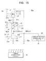
- Figure 15 is a circuit diagram of a third embodiment of the DC-DC converter according to the present invention. Also, Figs. 16A to 16J are timing charts of the circuit of Fig. 15.
- this DC-DC converter 20a is constituted by switch circuits 21a to 23a, capacitors 31a, 32a, and 33a, an external power supply 50 of the power supply voltage V cc , a power supply 60 for 0.25 V cc , and a timing generating circuit 70 generating the clock signals 0 ⁇ 1 to 0 ⁇ 7 at a timing shown in Figs. 16A to 16F.
- switch circuit 21a fixed contacts c1 and c2 of two on-off switches 111 and 112 are connected in parallel to one electrode of the capacitor 31a, the operational contact a1 of the switch 111 is connected to the external power supply 50, and the operational contact a2 of the switch 112 is connected to the output node ND OUT .
- the switch 111 is controlled on or off by the clock signal 0 ⁇ 1
- the switch 112 is controlled on or off by the clock signal 0 ⁇ 5.
- the switches 111 and 112 become the on state when the clock signal is at a high level and become the off state when it is at a low level.
- the fixed contacts c1, c2, and c3 of the three on-off switches 121, 122, and 123 are connected in parallel to the other electrode of the capacitor 31a, and the operational contact a1 of the switch 121 is connected to the operational contact a1 of the switch 131 of the switch circuit 23a.
- the operational contact a2 of the switch 122 is connected to the power supply 60 for 0.25 V cc , and the operational contact a3 of the switch 123 is grounded.
- the switch 121 is controlled on or off by the clock signal 0 ⁇ 2.
- the switch 122 is controlled on or off by the clock signal 0 ⁇ 6, and the switch 123 is controlled on or off by the clock signal 0 ⁇ 7.
- the switches 121, 122, and 123 become the on state when the clock signal is at a high level and become the off state when it is at a low level.
- the on-off control of these switches 121, 122, and 123 is sequentially carried out.
- the fixed contacts c1 and c2 of the two on-off switches 131 and 132 are connected in parallel to one electrode of the capacitor 32a, and the operational contact a2 of the switch 132 is connected to the output node ND OUT .
- the switch 131 is controlled on or off by the clock signal 0 ⁇ 3, and the switch 112 is controlled on or off by the clock signal 0 ⁇ 4.
- the switches 131 and 132 become the ON state when the clock signal is at a high level and become the off state when it is at a low level.
- the other electrode of the capacitor 32a is grounded.
- the switch circuits 21a to 23a are constituted by for example MOS system transistors.
- a stabilizing capacitor 33a for suppressing the voltage drop of the output node ND OUT by the load current I L is connected between the output node ND OUT and the ground line.
- capacitors 31a and 32a those having the same capacitance are used.
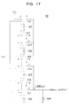
- Figure 17 is a circuit diagram of an example of the configuration of the power supply 60 for 0.25 V cc .
- This 0.25 V cc use power supply 60 is constituted by switch circuits 511 to 517 and capacitors 521 to 525 as shown in Fig. 17.
- the switch circuits 511 to 517 are constituted by for example MOS system transistors.
- the capacitors 521 to 524 those having the same capacitance are used.
- the operational contact a of the switch circuit 511 is connected to the supply line of the power supply voltage V cc , the operational contact b is connected to the output node ND OUT , and the fixed contact c is connected to one electrode of the capacitor 521.
- the operational contact a of the switch circuit 512 is connected to the operational contact a of the switch circuit 513, the operational contact b is grounded, and the fixed contact c is connected to the other electrode of the capacitor 521.
- the operational contact b of the switch circuit 513 is connected to the output node ND OUT , and the fixed contact c is connected to one electrode of the capacitor 522.
- the operational contact a of the switch circuit 514 is connected to the operational contact a of the switch circuit 515, the operational contact b is grounded, and the fixed contact c is connected to the other electrode of the capacitor 522.
- the operational contact b of the switch circuit 515 is connected to the output node ND OUT , and the fixed contact c is connected to one electrode of the capacitor 523.
- the operational contact a of the switch circuit 516 is connected to the operational contact a of the switch circuit 517, the operational contact b is grounded, and the fixed contact c is connected to the other electrode of the capacitor 523.
- the operational contact b of the switch circuit 517 is connected to the output node ND OUT , and the fixed contact c is connected to one electrode of the capacitor 524.
- the capacitor 525 is a stabilizing capacitor which is connected between the output node ND OUT and the ground line for suppressing the voltage drop of the output node ND OUT by a load current I L and stabilizing the same. Note that, it is not necessary to provide this stabilizing capacitor 525 when the parasitic capacitance of the output power supply line is large.
- the switch circuits 511 to 517 connect their fixed contacts c to the operational contact a when the clock signal 0 ⁇ 50 is at the V cc level (high level) and connect their fixed contacts c to the operational contact b when the clock signal 0 ⁇ 50 is at the ground level (low level).
- the four capacitors 521, 522, 523, and 524 are connected in series between the supply line of the power supply voltage V cc and the ground line and the capacitors 521 to 524 are charged.
- the timing generating circuit 70 first sets the clock signals 0 ⁇ 1 to 0 ⁇ 3 at a high level as shown in Fig. 16, holds the switches 111, 121, and 131 in the on state, connects two capacitors 31a and 32a in series between the external power supply 50 and the ground line, and makes them perform the charging with respect to the capacitors 31a and 32a.
- the clock signals 0 ⁇ 1 to 0 ⁇ 3 are switched to the low level, the clock signals 0 ⁇ 4 and 0 ⁇ 6 are set at a high level, the node ND2 is connected to the 0.25 V cc use power supply 60, and the charges of the capacitor 31a on the side connected to the node ND2 are discharged to the power supply 50.
- the clock signal 0 ⁇ 6 is switched to the low level, the clock signal 0 ⁇ 7 is set at a high level, the node ND2 is connected to the ground line, and the capacitor 31a is discharged so that the node ND1 exhibits 0.5 V cc and node ND2 exhibits 0V.
- the clock signal 0 ⁇ 5 is set at a high level
- the node ND1 is connected to the output node ND OUT
- 0.5 V cc (V cc /2) is supplied to the output node ND OUT .
- the clock signals 0 ⁇ 5 and 0 ⁇ 7 are switched to the low level, the clock signal 0 ⁇ 6 is set at a high level, the node ND2 is connected to 0.25 V cc use power supply 60, and the capacitor 31a is charged so that the potential of the node ND1 changes from 0.5 V cc to 0.75 V cc and the potential of the node ND2 changes from 0V to 0.25.
- the clock signal 0 ⁇ 6 is switched to the low level, the clock signal 0 ⁇ 1 is set at a high level, the node ND1 is connected to the external power supply 50, and the capacitor 31a is charged so that the potential of the node ND1 becomes V cc and the potential of the node ND2 becomes 0.5 V cc .
- the clock signals 0 ⁇ 1, 0 ⁇ 2, and 0 ⁇ 3 among the clock signals 0 ⁇ 1 to 0 ⁇ 7 are set at a high level at the timing generating circuit 70, and the clock signal 0 ⁇ 1 is supplied to the switch 111 of the switch circuit 21a, the clock signal 0 ⁇ 2 is supplied to the switch 121 of the switch circuit 22a, and the clock signal 0 ⁇ 3 is supplied to the switch circuit 131, respectively.
- the switches 111, 121, and 131 become the on state, the two capacitors 31a and 32a are connected in series between the external power supply 50 and the ground line, and the capacitors 31a and 32a are charged.
- the clock signals 0 ⁇ 1 to 0 ⁇ 3 are switched to the low level at the timing generating circuit 70, the clock signals 0 ⁇ 4 and 0 ⁇ 6 are set at a high level, the clock signal 0 ⁇ 4 is supplied to the switch 132 of the switch circuit 23a, and the clock signal 0 ⁇ 6 is supplied to the switch 122 of the switch circuit 22a, respectively.
- the node ND2 is connected to the 0.25 V cc use power supply 60, and the charges of the capacitor 31a on the side connected to the node ND2 are discharged to the power supply 60.
- a charge of 0.25 V cc (Cs1 + Cs2) flows into the power supply 50.
- the level of the node ND1 at this time is 0.75 V cc .
- Cs1 and Cs2 are parasitic capacitances of the nodes ND1 and ND2.
- the relationship with respect to the capacitance C 21 of the capacitor 31a is set as C 21 >> Cs1, Cs2.
- the clock signal 0 ⁇ 6 is switched to the low level at the timing generating circuit 70, the clock signal 0 ⁇ 7 is set at a high level, and the clock signal 0 ⁇ 7 is supplied to the switch 123 of the switch circuit 22a.
- the switch 122 becomes the off state, and the switch 123 becomes the on state.
- the node ND2 is connected to the ground line.
- the capacitor 31a is discharged so that the node ND1 exhibits 0.5 V cc and the node ND2 exhibits 0 V.
- the clock signal 0 ⁇ 5 is set at a high level at the timing generating circuit 70 and is supplied to the switch 112 of the switch circuit 21a.
- the switch 112 becomes the off state, and 0.5 V cc (V cc /2) is supplied to the output node ND OUT .
- the clock signals 0 ⁇ 5 and 0 ⁇ 7 are switched to the low level at the timing generating circuit 70, the clock signal 0 ⁇ 6 is set at a high level, and the clock signal 0 ⁇ 6 is supplied to the switch 122 of the switch circuit 22a.
- the node ND2 is connected to the 0.25 V cc use power supply 60.
- the capacitor 31a is charged so that the potential of the node ND1 changes from 0.5 V cc to 0.75 V cc , and the potential of the node ND2 changes from 0V to 0.25 V cc .
- the clock signal 0 ⁇ 6 is switched to the low level at the timing generating circuit 70, the clock signal 0 ⁇ 1 is set at a high level, and the clock signal 0 ⁇ 1 is supplied to the switch 111 of the switch circuit 21a.
- the switch 122 becomes the off state, and the switch 111 becomes the on state.
- the node ND1 is connected to the external power supply 50.
- the capacitor 31a is charged so that the potential of the node ND1 becomes V cc and the potential of the node ND2 becomes 0.5 V cc .
- a power supply 60 for potential lower than the external power supply 50 and the ground voltage source provision is made of switches 121, 122, and 123 respectively operationally connecting the external power supply 50 and the power supply 60 for low potential with the capacitors 31a and a circuit 70 for sequentially switching the connection and nonconnection state from the switch side connected to the external power supply to charge and discharge the capacitors 31a and sequentially switching the connection and nonconnection state from the switch side connected to the ground voltage source side to discharge the capacitors 31a and thereby perform a heat insulating charging, therefore there is the advantage that a low voltage source with which a stable output voltage Va can be obtained with a low power loss can be realized.
- the number of connections of the capacitors is not limited to that of the present example, and a variety of modifications are possible.
- the switch circuit can be constituted by for example a transmission gate of the CMOS type, but desirably a p-channel MOS transistor and n-channel MOS transistor are selected and used corresponding to the transmission potential.
- the capacitor desirably use is made of an external capacitance, high dielectric capacitance, MIM (metal-insulator-metal) configuration capacitance, DRAM trench or stack capacitance, planar capacitance, ferroelectric capacitance, or the like.
- MIM metal-insulator-metal
- a ferroelectric such as PZT has a relative dielectric constant larger than SiO 2 by two figures or more, and the parasitic capacitance can be sufficiently reduced.
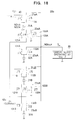
- Figure 18 is a circuit diagram of a fourth embodiment of the DC-DC converter according to the present invention.
- the difference of the present embodiment from the above third embodiment resides in that the switch circuits and capacitor columns of the system A and system B are connected in parallel, and they are respectively driven by the clock signals 0 ⁇ 1 to 0 ⁇ 7 and 0 ⁇ 1 ⁇ to 0 ⁇ 7 ⁇ having inverse phases to each other (deviated by ⁇ /2 phase).
- the ripple of the output node ND OUT accompanied with the load current I L can be lowered.
Landscapes
- Engineering & Computer Science (AREA)
- Power Engineering (AREA)
- Dc-Dc Converters (AREA)
- Dram (AREA)
Applications Claiming Priority (4)
| Application Number | Priority Date | Filing Date | Title |
|---|---|---|---|
| JP290070/95 | 1995-11-08 | ||
| JP29007095A JP3456074B2 (ja) | 1995-11-08 | 1995-11-08 | Dc−dcコンバータ |
| JP23073696A JPH1075568A (ja) | 1996-08-30 | 1996-08-30 | 電源回路 |
| JP230736/96 | 1996-08-30 |
Publications (2)
| Publication Number | Publication Date |
|---|---|
| EP0773622A2 true EP0773622A2 (fr) | 1997-05-14 |
| EP0773622A3 EP0773622A3 (fr) | 1997-07-23 |
Family
ID=26529502
Family Applications (1)
| Application Number | Title | Priority Date | Filing Date |
|---|---|---|---|
| EP96402383A Withdrawn EP0773622A3 (fr) | 1995-11-08 | 1996-11-08 | Circuit d'alimentation interne |
Country Status (6)
| Country | Link |
|---|---|
| US (1) | US5856918A (fr) |
| EP (1) | EP0773622A3 (fr) |
| KR (1) | KR970031198A (fr) |
| CN (1) | CN1061484C (fr) |
| ID (1) | ID18396A (fr) |
| SG (1) | SG48486A1 (fr) |
Cited By (13)
| Publication number | Priority date | Publication date | Assignee | Title |
|---|---|---|---|---|
| WO2014143366A1 (fr) * | 2013-03-15 | 2014-09-18 | Arctic Sand Technologies, Inc. | Protection de convertisseur de puissance à condensateur commuté |
| US9847712B2 (en) | 2013-03-15 | 2017-12-19 | Peregrine Semiconductor Corporation | Fault control for switched capacitor power converter |
| US9887622B2 (en) | 2014-03-14 | 2018-02-06 | Peregrine Semiconductor Corporation | Charge pump stability control |
| US10128745B2 (en) | 2014-03-14 | 2018-11-13 | Psemi Corporation | Charge balanced charge pump control |
| US10686380B2 (en) | 2011-12-19 | 2020-06-16 | Psemi Corporation | Switched-capacitor circuit control in power converters |
| US10686367B1 (en) | 2019-03-04 | 2020-06-16 | Psemi Corporation | Apparatus and method for efficient shutdown of adiabatic charge pumps |
| US10693368B2 (en) | 2014-03-14 | 2020-06-23 | Psemi Corporation | Charge pump stability control |
| US12107495B2 (en) | 2015-07-08 | 2024-10-01 | Psemi Corporation | Switched-capacitor power converters |
| US12212232B2 (en) | 2013-03-15 | 2025-01-28 | Psemi Corporation | Power supply for gate driver in switched-capacitor circuit |
| US12237765B2 (en) | 2015-03-13 | 2025-02-25 | Psemi Corporation | DC-DC transformer with inductor for the facilitation of adiabatic inter-capacitor charge transport |
| US12341424B2 (en) | 2011-05-05 | 2025-06-24 | Psemi Corporation | Power converters with modular stages |
| US12381482B2 (en) | 2011-05-05 | 2025-08-05 | Psemi Corporation | Power converter with modular stages connected by floating terminals |
| US12438135B2 (en) | 2011-10-18 | 2025-10-07 | Psemi Corporation | Multilayer power, converter with devices having reduced lateral current |
Families Citing this family (33)
| Publication number | Priority date | Publication date | Assignee | Title |
|---|---|---|---|---|
| DE19627197C1 (de) * | 1996-07-05 | 1998-03-26 | Siemens Ag | Vorrichtung zur Spannungsvervielfachung mit geringer Abhängigkeit der Ausgangsspannung von der Versorgungsspannung |
| IT1290168B1 (it) * | 1996-12-23 | 1998-10-19 | Consorzio Eagle | Pompa di carica a tensione negativa per memorie flash eeprom |
| IT1290167B1 (it) * | 1996-12-23 | 1998-10-19 | Consorzio Eagle | Pompa di carica in cmos ad alta corrente, in particolare per memorie flash eeprom |
| KR100256226B1 (ko) * | 1997-06-26 | 2000-05-15 | 김영환 | 레퍼런스 전압 발생 장치 |
| JP3223504B2 (ja) * | 1998-03-31 | 2001-10-29 | 日本電気株式会社 | 昇圧回路 |
| JP3872927B2 (ja) * | 2000-03-22 | 2007-01-24 | 株式会社東芝 | 昇圧回路 |
| JP3696125B2 (ja) * | 2000-05-24 | 2005-09-14 | 株式会社東芝 | 電位検出回路及び半導体集積回路 |
| US6696883B1 (en) * | 2000-09-20 | 2004-02-24 | Cypress Semiconductor Corp. | Negative bias charge pump |
| JP3594126B2 (ja) * | 2000-10-13 | 2004-11-24 | 日本電気株式会社 | 電流駆動回路 |
| US7336121B2 (en) * | 2001-05-04 | 2008-02-26 | Samsung Electronics Co., Ltd. | Negative voltage generator for a semiconductor memory device |
| US20030184360A1 (en) * | 2002-03-29 | 2003-10-02 | Yi-Ti Wang | Charge pump for flash memory with serially connected capacitors for preventing breakdown |
| US6861894B2 (en) * | 2002-09-27 | 2005-03-01 | Sandisk Corporation | Charge pump with Fibonacci number multiplication |
| FI114758B (fi) * | 2002-10-25 | 2004-12-15 | Nokia Oyj | Jännitekertoja |
| US6833753B2 (en) * | 2002-11-27 | 2004-12-21 | Texas Instruments Incorporated | Method and system for signal dependent boosting in sampling circuits |
| KR100518545B1 (ko) * | 2002-12-10 | 2005-10-04 | 삼성전자주식회사 | 고전압 스트레스를 감소시킬 수 있는 승압전압 발생회로및 승압전압 발생방법 |
| US20050077950A1 (en) * | 2003-10-14 | 2005-04-14 | Robinson Curtis B. | Negative charge pump |
| TWI298828B (en) * | 2005-06-29 | 2008-07-11 | Novatek Microelectronics Corp | Charge pump for generating arbitrary voltage level |
| KR100741978B1 (ko) * | 2005-09-16 | 2007-07-23 | 삼성에스디아이 주식회사 | 클럭신호 발생장치 및 이를 포함하는 유기 전계발광표시장치 |
| JP2008159736A (ja) * | 2006-12-22 | 2008-07-10 | Elpida Memory Inc | 半導体装置及びその電源供給方法 |
| US8115597B1 (en) * | 2007-03-07 | 2012-02-14 | Impinj, Inc. | RFID tags with synchronous power rectifier |
| US7894220B2 (en) * | 2008-03-27 | 2011-02-22 | Elite Semiconductor Memory Technology Inc. | Voltage generating circuit |
| US9001234B2 (en) | 2011-02-25 | 2015-04-07 | Intrinsix Corporation | Imager readout architecture utilizing A/D converters (ADC) |
| US9595558B2 (en) | 2013-11-12 | 2017-03-14 | Intrinsix Corporation | Photodiode architectures and image capture methods having a plurality of photodiode with a shared electrode |
| US9344660B2 (en) | 2011-02-25 | 2016-05-17 | Intrinsix Corporation | Foveal imager readout integrated circuit (ROIC) |
| KR101840379B1 (ko) | 2011-10-31 | 2018-03-21 | 에스케이하이닉스 주식회사 | 반도체 장치 |
| KR101315143B1 (ko) * | 2012-08-22 | 2013-10-14 | 전북대학교산학협력단 | 높은 승압 비를 갖는 고효율 dc/dc 컨버터 |
| US9787923B2 (en) * | 2014-01-13 | 2017-10-10 | Intrinsix Corporation | Correlated double sampled (CDS) pixel sense amplifier |
| JP6652457B2 (ja) * | 2016-06-29 | 2020-02-26 | キオクシア株式会社 | 昇圧回路 |
| CN108616216B (zh) * | 2016-12-09 | 2023-10-10 | 兆易创新科技集团股份有限公司 | 一种电荷泵泄放电路 |
| US10763746B1 (en) | 2019-08-01 | 2020-09-01 | Silanna Asia Pte Ltd | Series-parallel charge pump with NMOS devices |
| CN111338419B (zh) * | 2020-03-04 | 2021-05-25 | 长江存储科技有限责任公司 | 基准电压供应电路及其供应方法 |
| JP7522706B2 (ja) * | 2021-08-18 | 2024-07-25 | 矢崎総業株式会社 | 電源制御装置、電源装置、及び電源制御方法 |
| CN114362514A (zh) * | 2022-01-12 | 2022-04-15 | 南方科技大学 | 一种充电电路与充电系统 |
Family Cites Families (14)
| Publication number | Priority date | Publication date | Assignee | Title |
|---|---|---|---|---|
| DE405009C (de) * | 1922-11-25 | 1924-10-27 | Locomotive Firebox Company | Maschine zur Formgebung von Blechen durch eine Biegevorrichtung |
| GB1364618A (en) * | 1971-12-03 | 1974-08-21 | Seiko Instr & Electronics | Voltage boosters |
| US4106086A (en) * | 1976-12-29 | 1978-08-08 | Rca Corporation | Voltage multiplier circuit |
| US4199806A (en) * | 1978-01-18 | 1980-04-22 | Harris Corporation | CMOS Voltage multiplier |
| FR2437734A1 (fr) * | 1978-09-26 | 1980-04-25 | Thomson Csf | Amplificateur a capacites commutees, filtre a capacites commutees et filtre a transfert de charges comportant un tel amplificateur |
| US4433282A (en) * | 1981-12-08 | 1984-02-21 | Intersil | Monolithic voltage divider |
| DE3931596A1 (de) * | 1989-03-25 | 1990-10-04 | Eurosil Electronic Gmbh | Spannungsvervielfacherschaltung |
| JP2805210B2 (ja) * | 1989-06-09 | 1998-09-30 | 日本テキサス・インスツルメンツ株式会社 | 昇圧回路 |
| CH679901A5 (fr) * | 1989-06-20 | 1992-04-30 | Ernst Feller | |
| US5301097A (en) * | 1992-06-10 | 1994-04-05 | Intel Corporation | Multi-staged charge-pump with staggered clock phases for providing high current capability |
| JP2500422B2 (ja) * | 1993-02-10 | 1996-05-29 | 日本電気株式会社 | 半導体icチップ内蔵用の降圧回路 |
| US5397931A (en) * | 1993-03-31 | 1995-03-14 | Texas Instruments Deutschland Gmbh | Voltage multiplier |
| JPH07264842A (ja) * | 1994-03-22 | 1995-10-13 | Hitachi Ltd | 昇圧回路 |
| TW271011B (fr) * | 1994-04-20 | 1996-02-21 | Nippon Steel Corp |
-
1996
- 1996-11-05 US US08/743,825 patent/US5856918A/en not_active Expired - Fee Related
- 1996-11-07 SG SG1996011077A patent/SG48486A1/en unknown
- 1996-11-07 KR KR1019960052632A patent/KR970031198A/ko not_active Ceased
- 1996-11-08 CN CN96121658A patent/CN1061484C/zh not_active Expired - Fee Related
- 1996-11-08 ID IDP963235A patent/ID18396A/id unknown
- 1996-11-08 EP EP96402383A patent/EP0773622A3/fr not_active Withdrawn
Non-Patent Citations (1)
| Title |
|---|
| None |
Cited By (36)
| Publication number | Priority date | Publication date | Assignee | Title |
|---|---|---|---|---|
| US12341424B2 (en) | 2011-05-05 | 2025-06-24 | Psemi Corporation | Power converters with modular stages |
| US12381482B2 (en) | 2011-05-05 | 2025-08-05 | Psemi Corporation | Power converter with modular stages connected by floating terminals |
| US12438135B2 (en) | 2011-10-18 | 2025-10-07 | Psemi Corporation | Multilayer power, converter with devices having reduced lateral current |
| US10686380B2 (en) | 2011-12-19 | 2020-06-16 | Psemi Corporation | Switched-capacitor circuit control in power converters |
| US12176815B2 (en) | 2011-12-19 | 2024-12-24 | Psemi Corporation | Switched-capacitor circuit control in power converters |
| US12143010B2 (en) | 2013-03-15 | 2024-11-12 | Psemi Corporation | Protection of switched capacitor power converter |
| CN105229908B (zh) * | 2013-03-15 | 2018-10-19 | 北极砂技术有限公司 | 开关电容器功率转换器的保护 |
| GB2526492A (en) * | 2013-03-15 | 2015-11-25 | Arctic Sand Technologies Inc | Protection of switched capacitor power converter |
| US12212232B2 (en) | 2013-03-15 | 2025-01-28 | Psemi Corporation | Power supply for gate driver in switched-capacitor circuit |
| CN105229908A (zh) * | 2013-03-15 | 2016-01-06 | 北极砂技术有限公司 | 开关电容器功率转换器的保护 |
| US9847712B2 (en) | 2013-03-15 | 2017-12-19 | Peregrine Semiconductor Corporation | Fault control for switched capacitor power converter |
| US10666134B2 (en) | 2013-03-15 | 2020-05-26 | Psemi Corporation | Fault control for switched capacitor power converter |
| WO2014143366A1 (fr) * | 2013-03-15 | 2014-09-18 | Arctic Sand Technologies, Inc. | Protection de convertisseur de puissance à condensateur commuté |
| US12113438B2 (en) | 2013-03-15 | 2024-10-08 | Psemi Corporation | Protection of switched capacitor power converter |
| US11901817B2 (en) | 2013-03-15 | 2024-02-13 | Psemi Corporation | Protection of switched capacitor power converter |
| GB2526492B (en) * | 2013-03-15 | 2021-01-27 | Arctic Sand Technologies Inc | Protection of switched capacitor power converter |
| US10938299B2 (en) | 2013-03-15 | 2021-03-02 | Psemi Corporation | Fault detector for voltage converter |
| US11025164B2 (en) | 2013-03-15 | 2021-06-01 | Psemi Corporation | Fault detector for voltage converter |
| US11031864B2 (en) | 2014-03-14 | 2021-06-08 | Psemi Corporation | Charge pump stability control |
| US10348195B2 (en) | 2014-03-14 | 2019-07-09 | Psemi Corporation | Charge balanced charge pump control |
| US11177735B2 (en) | 2014-03-14 | 2021-11-16 | Psemi Corporation | Charge pump stability control |
| US11336175B2 (en) | 2014-03-14 | 2022-05-17 | Psemi Corporation | Charge balanced charge pump control |
| US11496046B2 (en) | 2014-03-14 | 2022-11-08 | Psemi Corporation | Charge pump stability control |
| US11527952B2 (en) | 2014-03-14 | 2022-12-13 | Psemi Corporation | Charge pump stability control |
| US9887622B2 (en) | 2014-03-14 | 2018-02-06 | Peregrine Semiconductor Corporation | Charge pump stability control |
| US11784561B2 (en) | 2014-03-14 | 2023-10-10 | Psemi Corporation | Charge pump stability control |
| US10693368B2 (en) | 2014-03-14 | 2020-06-23 | Psemi Corporation | Charge pump stability control |
| US10027224B2 (en) | 2014-03-14 | 2018-07-17 | Psemi Corporation | Charge pump stability control |
| US10128745B2 (en) | 2014-03-14 | 2018-11-13 | Psemi Corporation | Charge balanced charge pump control |
| US10574140B2 (en) | 2014-03-14 | 2020-02-25 | Psemi Corporation | Charge balanced charge pump control |
| US10454368B2 (en) | 2014-03-14 | 2019-10-22 | Psemi Corporation | Charge pump stability control |
| US12237765B2 (en) | 2015-03-13 | 2025-02-25 | Psemi Corporation | DC-DC transformer with inductor for the facilitation of adiabatic inter-capacitor charge transport |
| US12107495B2 (en) | 2015-07-08 | 2024-10-01 | Psemi Corporation | Switched-capacitor power converters |
| US11075576B2 (en) | 2019-03-04 | 2021-07-27 | Psemi Corporation | Apparatus and method for efficient shutdown of adiabatic charge pumps |
| US10686367B1 (en) | 2019-03-04 | 2020-06-16 | Psemi Corporation | Apparatus and method for efficient shutdown of adiabatic charge pumps |
| US11671004B2 (en) | 2019-03-04 | 2023-06-06 | Psemi Corporation | Power converter with multi-level topology |
Also Published As
| Publication number | Publication date |
|---|---|
| CN1061484C (zh) | 2001-01-31 |
| SG48486A1 (en) | 1998-04-17 |
| CN1159094A (zh) | 1997-09-10 |
| US5856918A (en) | 1999-01-05 |
| EP0773622A3 (fr) | 1997-07-23 |
| KR970031198A (ko) | 1997-06-26 |
| ID18396A (id) | 1998-04-02 |
Similar Documents
| Publication | Publication Date | Title |
|---|---|---|
| US5856918A (en) | Internal power supply circuit | |
| JP4257064B2 (ja) | 昇圧電位発生回路及び制御方法 | |
| JP2755047B2 (ja) | 昇圧電位発生回路 | |
| US7920018B2 (en) | Booster circuit | |
| US6912159B2 (en) | Boosting circuit and non-volatile semiconductor storage device containing the same | |
| KR101504587B1 (ko) | 음 전원전압 발생회로 및 이를 포함하는 반도체 집적회로 | |
| JPH09198887A (ja) | 高電圧発生回路 | |
| US7365591B2 (en) | Voltage generating circuit | |
| JPH09231752A (ja) | 内部電位発生回路および昇圧電位発生ユニット | |
| JP5537307B2 (ja) | チャージポンプ回路、不揮発性メモリ、データ処理装置、及びマイクロコンピュータ応用システム | |
| JP3505324B2 (ja) | チャージポンプ回路 | |
| JP2002261239A (ja) | 不揮発性半導体メモリ装置の昇圧回路 | |
| EP1278202A2 (fr) | Dispositif de mémoire à semiconducteurs non-volatile | |
| KR19990050472A (ko) | 승압전압 발생회로 | |
| JP3456074B2 (ja) | Dc−dcコンバータ | |
| US7808303B2 (en) | Booster circuit | |
| JP2008198985A (ja) | 昇圧回路 | |
| JPH11503261A (ja) | 電圧増倍のための装置 | |
| KR100253726B1 (ko) | 승압 회로 및 강압 회로 | |
| JP2002237192A (ja) | 負昇圧回路及び不揮発性半導体記憶装置 | |
| JP4730638B2 (ja) | 半導体装置 | |
| JPH10283790A (ja) | 半導体装置 | |
| JPH01134796A (ja) | 不揮発性半導体記憶装置 | |
| JP3012634B1 (ja) | 半導体昇圧回路 | |
| JPH1075568A (ja) | 電源回路 |
Legal Events
| Date | Code | Title | Description |
|---|---|---|---|
| PUAI | Public reference made under article 153(3) epc to a published international application that has entered the european phase |
Free format text: ORIGINAL CODE: 0009012 |
|
| AK | Designated contracting states |
Kind code of ref document: A2 Designated state(s): DE FR GB |
|
| PUAL | Search report despatched |
Free format text: ORIGINAL CODE: 0009013 |
|
| RIN1 | Information on inventor provided before grant (corrected) |
Inventor name: LI, AKIRA Inventor name: SONEDA, MITSUO |
|
| AK | Designated contracting states |
Kind code of ref document: A3 Designated state(s): DE FR GB |
|
| 17P | Request for examination filed |
Effective date: 19980107 |
|
| 17Q | First examination report despatched |
Effective date: 19990504 |
|
| STAA | Information on the status of an ep patent application or granted ep patent |
Free format text: STATUS: THE APPLICATION IS DEEMED TO BE WITHDRAWN |
|
| 18D | Application deemed to be withdrawn |
Effective date: 20030603 |