EP0775332B1 - Sicherheitsschalteranordnung - Google Patents
Sicherheitsschalteranordnung Download PDFInfo
- Publication number
- EP0775332B1 EP0775332B1 EP96905792A EP96905792A EP0775332B1 EP 0775332 B1 EP0775332 B1 EP 0775332B1 EP 96905792 A EP96905792 A EP 96905792A EP 96905792 A EP96905792 A EP 96905792A EP 0775332 B1 EP0775332 B1 EP 0775332B1
- Authority
- EP
- European Patent Office
- Prior art keywords
- actuator
- circuitbreaker
- arrangement according
- switch
- computer
- Prior art date
- Legal status (The legal status is an assumption and is not a legal conclusion. Google has not performed a legal analysis and makes no representation as to the accuracy of the status listed.)
- Expired - Lifetime
Links
Images

Classifications
-
- G—PHYSICS
- G05—CONTROLLING; REGULATING
- G05B—CONTROL OR REGULATING SYSTEMS IN GENERAL; FUNCTIONAL ELEMENTS OF SUCH SYSTEMS; MONITORING OR TESTING ARRANGEMENTS FOR SUCH SYSTEMS OR ELEMENTS
- G05B19/00—Program-control systems
- G05B19/02—Program-control systems electric
- G05B19/04—Program control other than numerical control, i.e. in sequence controllers or logic controllers
- G05B19/048—Monitoring; Safety
-
- G—PHYSICS
- G05—CONTROLLING; REGULATING
- G05B—CONTROL OR REGULATING SYSTEMS IN GENERAL; FUNCTIONAL ELEMENTS OF SUCH SYSTEMS; MONITORING OR TESTING ARRANGEMENTS FOR SUCH SYSTEMS OR ELEMENTS
- G05B19/00—Program-control systems
- G05B19/02—Program-control systems electric
- G05B19/04—Program control other than numerical control, i.e. in sequence controllers or logic controllers
- G05B19/042—Program control other than numerical control, i.e. in sequence controllers or logic controllers using digital processors
- G05B19/0423—Input/output
- G05B19/0425—Safety, monitoring
-
- G—PHYSICS
- G05—CONTROLLING; REGULATING
- G05B—CONTROL OR REGULATING SYSTEMS IN GENERAL; FUNCTIONAL ELEMENTS OF SUCH SYSTEMS; MONITORING OR TESTING ARRANGEMENTS FOR SUCH SYSTEMS OR ELEMENTS
- G05B9/00—Safety arrangements
- G05B9/02—Safety arrangements electric
- G05B9/03—Safety arrangements electric with multiple-channel loop, i.e. redundant control systems
-
- G—PHYSICS
- G05—CONTROLLING; REGULATING
- G05B—CONTROL OR REGULATING SYSTEMS IN GENERAL; FUNCTIONAL ELEMENTS OF SUCH SYSTEMS; MONITORING OR TESTING ARRANGEMENTS FOR SUCH SYSTEMS OR ELEMENTS
- G05B2219/00—Program-control systems
- G05B2219/20—Pc systems
- G05B2219/23—Pc programming
- G05B2219/23454—Execute program in fast mode, real system has no time to respond
-
- G—PHYSICS
- G05—CONTROLLING; REGULATING
- G05B—CONTROL OR REGULATING SYSTEMS IN GENERAL; FUNCTIONAL ELEMENTS OF SUCH SYSTEMS; MONITORING OR TESTING ARRANGEMENTS FOR SUCH SYSTEMS OR ELEMENTS
- G05B2219/00—Program-control systems
- G05B2219/20—Pc systems
- G05B2219/24—Pc safety
- G05B2219/24184—Redundant I-O, software comparison of both channels
-
- G—PHYSICS
- G05—CONTROLLING; REGULATING
- G05B—CONTROL OR REGULATING SYSTEMS IN GENERAL; FUNCTIONAL ELEMENTS OF SUCH SYSTEMS; MONITORING OR TESTING ARRANGEMENTS FOR SUCH SYSTEMS OR ELEMENTS
- G05B2219/00—Program-control systems
- G05B2219/20—Pc systems
- G05B2219/24—Pc safety
- G05B2219/24188—Redundant processors run different programs
-
- G—PHYSICS
- G05—CONTROLLING; REGULATING
- G05B—CONTROL OR REGULATING SYSTEMS IN GENERAL; FUNCTIONAL ELEMENTS OF SUCH SYSTEMS; MONITORING OR TESTING ARRANGEMENTS FOR SUCH SYSTEMS OR ELEMENTS
- G05B2219/00—Program-control systems
- G05B2219/20—Pc systems
- G05B2219/25—Pc structure of the system
- G05B2219/25458—Opto isolation, optical separation
Definitions
- the invention relates to a safety switch arrangement according to German laid-open specification DE-A-44 41 070 (date of disclosure: May 30, 1996).
- the two-channel safety switch arrangement described there has actuators with switch-like means consisting of semiconductor elements. This In contrast to relays, semiconductor elements are not susceptible to wear Contacts.
- each computer unit having two bidirectional supply lines is connected to the actuator.
- the computing units which are preferably designed as controllers, can be used as standard products upstream of the actuators at low cost without additional circuitry become.
- Computer units for control are already in a large number of sensors integrated sensor functions. In this case, these computing units the additional functions required for the safety switch arrangement process so that the circuit complexity of the sensor is further reduced becomes.
- the complete control and function monitoring of the actuators takes place centrally in the computer units. So that the function monitoring of the Transmission of the sensor signals is physically separated, are for transmission the switching impulses of the sensor and for the transmission of test impulses for the function check separate bidirectional from the computer unit to the actuator Supply lines are provided, which increases the functional reliability of the arrangement.
- the bidirectional leads do not transmit the switching impulses and test impulses only to the actuator but receive feedback from it. From this Acknowledgment is also obtained for information as to whether the functions of the actuator and the supply lines are error-free. Because of the different Feedback can quickly and safely localize any errors that may occur and be classified.
- the Computer units briefly changed the switching states and the feedback checked in the computer units whether the functions of the evaluation channels and the actuators are error-free. This change in the switching states takes place so briefly that the operating condition of the work equipment does not change, i.e. the operation of the work equipment is not affected by the functional check impaired.
- Another advantage of this arrangement is that the Function check parameters can be easily set using the computer units are.
- the invention has for its object the scope of the functional check increase with the least possible circuitry.
- the voltage monitoring unit which is connected to the switches in the supply lines are led, which lead to the actuators, the operating voltages the computer units checked so that outgoing from the computer units incorrect control signals due to overvoltage or undervoltage, that can lead to a dangerous failure of the switches can be.
- the function monitoring can advantageously be carried out in such a way that the read-back lines are no longer fed back to both computing units must be, which reduces the circuitry.
- the sensor via a two-channel supply line with each computer unit connected, whereby the signals from the sensor to the computer unit can be monitored.
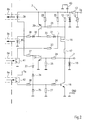
- Fig. 1 shows a safety switch assembly 1 for switching the on and off Power supply of a work equipment, not shown. Switching on and off of the work equipment takes place by means of a sensor signal S.
- the sensor is preferably designed as a light barrier, in its housing the complete Safety switch arrangement is integrated.
- the sensor can be used, for example, to monitor a protective field in the area of the work equipment. It has two signal states, namely Protective field free (sensor active) and protective field not free (sensor inactive).
- the binary sensor signal S is the two evaluation channels 2 of the safety switch arrangement 1 fed.
- Each evaluation channel 2 has a feed line 2a, 2b, which connects the sensor directly to an actuator 3.
- the actuator 3 has switch-like means consisting of semiconductor elements.
- the actuator 3 is a computer unit 4 connected upstream, which as a controller, preferably as Microcontroller, is trained.
- Each computer unit 4 is via a separate feed line 2a, 2b connected to the sensor, whereby the sensor signal via the Computer units 4 can be monitored.
- the computer units 4 are coupled via a bidirectional feed line 5.
- the Hardware of the controller is constructed identically, while its software is different is trained.
- the controllers are accordingly in terms of hardware homogeneously redundant, while the software is diversified is.
- the computing units 4 operate in the master-slave mode, the Master controls the communication of the computing units 4.
- the mutual The computer units 4 are advantageously checked in an asynchronous manner Delayed operation.
- bidirectional feed lines 5a, 5b and 6a, 6b coupled to the computer unit 4 two bidirectional feed lines 5a, 5b and 6a, 6b coupled. Via the first supply line 5a, 5b can be read back the switching pulses that correspond to the current signal state of the sensor correspond to the actuator 3. About all supply lines 5a, 5b, 6a, 6b are test pulses to the actuator 3 for its function check transfer.
- the bidirectional feed lines 5a, 5b, 6a, 6b each consist of a signal line 5a, 6a for the transmission of information to the actuator 3 and a readback line 5b, 6b for feedback from Actuator 3 to the computer unit 4.
- Each actuator 3 has a switching output 7. Only if both switching outputs 7 are active, i.e. if both switching outputs 7 have the signal states "protective field free "of the sensor, the work equipment is switched on.
- the safety switch arrangement 1 has a voltage monitoring unit 8, on the inputs of which leads 9a are led from the outputs of the computer units 4.
- the voltage monitoring unit 8 is preferably formed by an integrated circuit (IC).
- Another feed line 9b is led from an input of the voltage monitoring unit 8 to a reference voltage potential U re1 .
- a feed line 10 is routed to switch 11 in the signal lines 5a.
- the switches 11 are preferably designed as transistors.
- the voltage monitoring unit 8 is used to check whether the operating voltages of the computer units 4 in a predetermined target value range are located. If this is not the case, then the lead 10 two switches 11 opened, the work equipment accordingly deactivated. Thereby it is ensured that no incorrect control signals from the computer units 4 due to overvoltages or undervoltage.
- FIG. 2 shows a block diagram of an actuator 3.
- a varistor 12 On the exit side of the actuator 3 are a varistor 12, a resistor 13 and a suppressor diode 14 provided to protect transient overvoltages.
- the resistance 13 serves for the time delay of overvoltage pulses, so that the faster suppressor diode 14 does not respond before the varistor 12.
- Overvoltage protection leads a supply line to a via a resistor 15 P-channel MOS field effect transistor 16, which forms the switch-like means.
- the switch-like means is via a resistor 17 to the switching output 7 guided.
- a lead leads from resistor 17 to a transistor 19, which is connected to ground potential GND.
- the transistor 19 is turned on a suppressor diode 18 protected from overvoltages.
- the transistor 16 is through the resistors 15 and 20 as a first constant current source connected, whereby the current to a maximum value during short-circuit tests is limited.
- the resistor 20 is like the diode 21 and resistors 22, 23 on the led switch-like means. Resistors 24 and 25 are on the switching output 7 led. Resistors 26 and 27 are connected to transistor 19. Resistances 28 and 29 are between the resistor 15 and a transistor 30 switched. The transistor 30 regulates via the diode 21 and the resistor 22 the transistor 16, so that there is a second constant current source, the over the diode 32 is led to the readback line 5b.
- a transistor 31 is provided for measuring the voltage at the collector of transistor 19.
- the transistor 31 represents a starting current limitation for the transistor, ie it limits the current flow of the transistor 19 if the switch output 7 were short-circuited to the supply voltage U B. This protects the transistor 19 from destruction.
- the switching output is made by means of a Zener diode 33 and a diode 34 7 switched to ground potential GND.
- Resistors 36 and 37 are the transmission elements for the readback lines 5b, 6b upstream.
- the receiving elements of the signal lines 5a, 5b are Resistors 23, 38 connected downstream.
- the transmission elements for the readback lines 6b and 5b are from optocouplers 39, 40 formed.
- the receiving elements for the signal lines 5a, 6a are from Optocouplers 41 and 42 formed.
- the signal lines 5a, 6a are switched so that the computer units are in the reset state 4 the transistors 16 and 19 are high-resistance. So nobody can of these transistors 16, 19 are destroyed by an external short circuit before the computing units 4 are in operation.
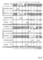
- the functional check of evaluation channels 2 is carried out independently of the current one Sensor state, i.e. regardless of whether the sensor is active or inactive. This is indicated by the hatched areas in FIG. 3.
- the implementation the function check is controlled by the computer units 4.
- the computing units work in master-slave mode. This means that a Computer unit 4 as master controls the communication via the leads 5. Communication takes the form of two-bit parallel communication, i.e. each computer unit 4 has a transmission and reception line 5.
- the functional control of the computer units 4 is carried out mutually via a time-out function. If one computing unit 4 detects a signal from the other Computing unit 4 does not respond in time, the missing answer is considered Interpreted error.
- the function check is carried out in the two Evaluation channels delayed.
- a Computer unit 4 for performing the functional check by the master for the sake of clarity, the time delay between two function checks is not shown in Fig. 3.
- test section I The functional check is divided into test sections I, II, III, IV, During The first three test sections I, II, III are checked to see whether there is any in actuator 3 itself There is a fault. In test section IV the function of the voltage monitoring unit 8 and the switch 11 checked.
- the signal sequences shown in FIG. 3 represent the error-free case.
- test section I the signal lines 5a, 6a are activated.
- the readback line 5b In the fault-free case, the readback line 5b must be in the active state and the read-back line 6b assume the state inactive.
- the transistor 16 connected by resistors 15 and 20 as a constant current source.
- a capacitor 43 is provided as an energy store, so that the supply Power supply is not burdened by this.
- the signal lines 5a, 6a are time-shifted activated.
- the read-back line 5b remains in the inactive state, while the readback line 6b is only inactive during test section III is, but not during test section II.
- readback lines 5b, 6b result during the test sections I, II, III switching states, of the states shown in Fig. 3 differ.
- the transistors 16, 19 can be alloyed or high-resistance. There may also be a short against ground potential GND or the supply voltage U B. Finally, the voltage monitoring unit 8 may be defective or the switching outputs 7 may be cross-connected to one another.
- the transistor 16 If the transistor 16 is alloyed in the event of a fault and can no longer be switched off, current flows when the transistor 19 is switched on until the resistor 17 forming a fuse responds and disconnects the switching output 7 from the supply voltage U B. Before the fuse responds, the faulty evaluation channel 2 can still go into the safe state, ie switch off the work equipment.
- test section IV the voltage monitoring of the computer unit 4 checked.
- the computer unit 4 simulates an overvoltage pulse (Signal lines 5a, 6a active), whereupon the feed line 9a in the faultless case is activated.
- the switching states of the signal lines are used for cyclical function monitoring 5a, 6a briefly changed.
- the individual time intervals "1" to "8" lie in the range of 50 - 150 ⁇ s. These time intervals are so short that the changes in the switching states carried out within these intervals the signal lines 5a, 6b no change due to the inertia of the working medium can cause its operating state.
- the repetition time of the Cyclic function monitoring is in the range 5 - 15 ms, preferably they 10 ms. It is particularly advantageous that the cyclical function monitoring is controlled by the computer units 4. About the software in the Computer units 4 can repeat the cyclical function monitoring can be varied, for example by overloading the computer units 4 to avoid.
Landscapes
- Physics & Mathematics (AREA)
- General Physics & Mathematics (AREA)
- Engineering & Computer Science (AREA)
- Automation & Control Theory (AREA)
- Testing Electric Properties And Detecting Electric Faults (AREA)
- Safety Devices In Control Systems (AREA)
- Electronic Switches (AREA)
Description
- Fig.1
- Ein Blockschaltbild der Sicherheitsschalteranordnung
- Fig. 2
- Ein Blockschaltbild des Aktors
- Fig. 3
- Ein Impulsdiagramm der Signalzustände der bidirektionalen Zuleitungen.
Claims (9)
- Sicherheitsschalteranordnung (1) zum Ein- und Ausschalten der Stromversorgung eines Arbeitsmittels mittels eines Sensorsignals, welches dem Arbeitsmittel über zwei Auswertekanäle (2) zugeführt wird, wobei jeder Auswertekanal einen Aktor (3) mit aus Halbleiterelementen bestehenden schalterartigen Mitteln aufweist, welchem eine Rechnereinheit (4) vorgeschaltet ist, die mit dem Aktor (3) über zwei bidirektionale Zuleitungen (5a, 6b, 6a, 6b) verbunden ist, wobei über die erste Zuleitung (5a, 5b) rücklesbar Schaltimpulse von der Rechnereinheit (4) zum Aktor (3) übertragen werden und dort einen Schaltvorgang auslösen, und wobei über die zweite Zuleitung (6a, 6b) rücklesbar Testimpulse von der Rechnereinheit (4) zum Aktor (3) zu dessen Funktionsüberprüfung übertragen werden, wobei die Rechnereinheiten (4) über eine bidirektionale Zuleitung (5) zu deren Funktionsüberprüfung verbunden sind, und wobei von den Rechnereinheiten (4) zur Funktionsüberprüfung der Aktoren (3) die Schaltzustände der schalterartigen Mittel so kurzzeitig geändert werden, daß sich der Betriebszustand des Arbeitsmittels aufgrund seiner Trägheit nicht ändert, und wobei die Zuleitungen (5a) jeweils einen Schalter (11) aufweisen, die mittels einer Spannungsüberwachungseinheit (8) geöffnet werden, sobald sich die Betriebspannung der Rechnereinheiten (4) außerhalb eines vorgegebenen Sollwertbereichs befinden.
- Sicherheitsschalteranordnung nach Anspruch 1, bei der die Schalter (11) von jeweils einem Transistor gebildet sind.
- Sicherheitsschalteranordnung nach Anspruch 1 oder 2, bei der von jeder Rechnereinheit (4) eine Zuleitung (2a, 2b) zum Sensor geführt ist.
- Sicherheitsschalteranordnung nach Anspruch 1 - 3, bei der die Rechnereinheiten (4) im Master-Slave Betrieb arbeiten.
- Sicherheitsschalteranordnung nach einem der Ansprüche 1 - 4, bei der die Funktionsüberprüfung unabhängig vom Signalzustand des Sensors erfolgt.
- Sicherheitsschalteranordnung nach einem der Ansprüche 1- 5, bei der die Funktionsüberprüfung aus vier nacheinander ablaufenden Testabschnitten besteht, wobei die ersten drei Testabschnitte zur Überprüfung des Aktors (3) vorgesehen sind und der vierte Testabschnitt zur Überprüfung der Betriebsspannungen der Rechnereinheiten (4) vorgesehen ist.
- Sicherheitsschalteranordnung nach einem der Ansprüche 1 - 6, bei der das schalterartige Mittel von einem MOS-Feldeffekttransistor (16) gebildet ist.
- Sicherheitsschalteranordnung nach Anspruch 7, bei welcher der MOS-Feldeffekttransistor (16) durch Widerstände (15) und (20) als erste Konstantstromquelle beschaltet ist.
- Sicherheitsschalteranordnung nach Anspruch 7 oder 8, bei der ein Transistor (30) über einen Widerstand (22) und eine Diode (21) auf den MOS-Feldeffekttransistor (16) geführt ist, wobei der Transistor (30) den MOS-Feldeffekttransistor (16) über den Widerstand (22) und die Diode (21) regelt, so daß sich eine zweite Konstantstromquelle ergibt.
Applications Claiming Priority (3)
| Application Number | Priority Date | Filing Date | Title |
|---|---|---|---|
| DE19508841 | 1995-03-11 | ||
| DE19508841A DE19508841C2 (de) | 1994-11-18 | 1995-03-11 | Sicherheitsschalteranordnung |
| PCT/EP1996/000769 WO1996028769A1 (de) | 1995-03-11 | 1996-02-24 | Sicherheitsschalteranordnung |
Publications (2)
| Publication Number | Publication Date |
|---|---|
| EP0775332A1 EP0775332A1 (de) | 1997-05-28 |
| EP0775332B1 true EP0775332B1 (de) | 2000-05-10 |
Family
ID=7756424
Family Applications (1)
| Application Number | Title | Priority Date | Filing Date |
|---|---|---|---|
| EP96905792A Expired - Lifetime EP0775332B1 (de) | 1995-03-11 | 1996-02-24 | Sicherheitsschalteranordnung |
Country Status (4)
| Country | Link |
|---|---|
| US (1) | US5777834A (de) |
| EP (1) | EP0775332B1 (de) |
| AT (1) | ATE192859T1 (de) |
| WO (1) | WO1996028769A1 (de) |
Cited By (1)
| Publication number | Priority date | Publication date | Assignee | Title |
|---|---|---|---|---|
| DE10059751A1 (de) * | 2000-11-30 | 2002-06-20 | Leuze Lumiflex Gmbh & Co | Verfahren und Schaltungsanordnung zur Überprüfung eines Ausganges eines elektrischen Bauteils |
Families Citing this family (13)
| Publication number | Priority date | Publication date | Assignee | Title |
|---|---|---|---|---|
| JPH11161326A (ja) | 1997-11-26 | 1999-06-18 | Fanuc Ltd | 数値制御装置 |
| ATE239930T1 (de) | 1998-11-09 | 2003-05-15 | Siemens Ag | Verfahren zum überprüfen einer ausgabeeinheit |
| US6275364B1 (en) * | 1999-02-26 | 2001-08-14 | Micron Technology Inc. | Method of enabling system operation |
| US6256180B1 (en) * | 1999-02-26 | 2001-07-03 | Micron Technology, Inc. | Apparatus for enabling system operation |
| US6795926B1 (en) | 1999-05-28 | 2004-09-21 | Dell Usa, L.P. | Prevention of power state change in response to chassis intrusion when computer system is not in powered up power state |
| EP1196975A1 (de) * | 1999-07-16 | 2002-04-17 | Siemens Aktiengesellschaft | Einrichtung zum kurzschliessen |
| WO2001027954A1 (de) * | 1999-10-08 | 2001-04-19 | Siemens Aktiengesellschaft | Aktoreinheit mit mindestens zwei schützen und einer sicheren ansteuereinheit |
| DE10127233C1 (de) * | 2001-05-22 | 2002-11-28 | Pilz Gmbh & Co | Sicherheitsschaltmodul und Verfahren zur Prüfung des Abschaltvermögens eines Schaltelements in einem Sicherheitsschaltmodul |
| DE10203921B4 (de) * | 2002-01-31 | 2015-11-12 | Bayerische Motoren Werke Aktiengesellschaft | Steuergerät |
| US7065662B2 (en) * | 2003-03-10 | 2006-06-20 | Dell Products L.P. | Information handling system featuring a power-based current limiting circuit |
| DE10330916A1 (de) * | 2003-07-04 | 2005-02-03 | Pilz Gmbh & Co. Kg | Vorrichtung und Verfahren zum automatisierten Steuern eines Betriebsablaufs bei einer technischen Anlage |
| EP2407992B1 (de) * | 2010-07-15 | 2013-09-04 | ABB Technology AG | Antriebs- und Steuerungseinheit für eine Nieder- oder Mittelspannungsvorrichtung |
| DE102013112488A1 (de) * | 2013-11-13 | 2015-05-13 | Pilz Gmbh & Co. Kg | Sicherheitssteuerung mit konfigurierbaren Eingängen |
Family Cites Families (12)
| Publication number | Priority date | Publication date | Assignee | Title |
|---|---|---|---|---|
| GB2007883B (en) * | 1977-09-23 | 1982-02-10 | Post Office | Power supplies |
| DE3024370C2 (de) * | 1980-06-27 | 1987-01-02 | Siemens AG, 1000 Berlin und 8000 München | Redundantes Steuersystem |
| GB2183113B (en) * | 1983-10-29 | 1987-12-02 | M L Engineering | Failsafe electrical power supply |
| DE3513357A1 (de) * | 1985-04-15 | 1986-10-16 | Fernsprech- und Signalbau KG Schüler & Vershoven, 4300 Essen | Schaltungsanordnung, insbesondere fuer einen sicherheitskoppelschalter im untertagebergbau |
| DE3639065C2 (de) * | 1986-11-14 | 1997-01-09 | Bosch Gmbh Robert | Verfahren zur Überwachung eines rechnergesteuerte Stellglieder ansteuernden Prozeßrechners |
| DE3701714A1 (de) * | 1987-01-22 | 1988-08-04 | Bosch Gmbh Robert | Verfahren und vorrichtung zur ueberwachung rechnergesteuerter stellglieder |
| DE3812760C2 (de) * | 1988-04-16 | 1996-10-24 | Vdo Schindling | Verfahren und Anordnung zur Überwachung eines Sollwertgebers |
| JP2873843B2 (ja) * | 1989-12-11 | 1999-03-24 | 株式会社 ユニシアジェックス | 自動車用制御装置のcpuバックアップ装置 |
| GB2249229A (en) * | 1990-10-09 | 1992-04-29 | Christopher James Cook | Mains overvoltage and undervoltage protection |
| DE4321971A1 (de) * | 1992-07-09 | 1994-01-13 | Siemens Ag | Schaltungsanordnung |
| DE4242792C2 (de) * | 1992-12-17 | 1997-02-06 | Sick Optik Elektronik Erwin | Sicherheitsschalteranordnung |
| DE4441070C2 (de) * | 1994-11-18 | 1997-12-11 | Leuze Electronic Gmbh & Co | Sicherheitsschalteranordnung |
-
1996
- 1996-02-24 AT AT96905792T patent/ATE192859T1/de active
- 1996-02-24 EP EP96905792A patent/EP0775332B1/de not_active Expired - Lifetime
- 1996-02-24 WO PCT/EP1996/000769 patent/WO1996028769A1/de not_active Ceased
- 1996-02-24 US US08/732,456 patent/US5777834A/en not_active Expired - Lifetime
Cited By (2)
| Publication number | Priority date | Publication date | Assignee | Title |
|---|---|---|---|---|
| DE10059751A1 (de) * | 2000-11-30 | 2002-06-20 | Leuze Lumiflex Gmbh & Co | Verfahren und Schaltungsanordnung zur Überprüfung eines Ausganges eines elektrischen Bauteils |
| DE10059751B4 (de) * | 2000-11-30 | 2004-09-30 | Leuze Lumiflex Gmbh + Co. Kg | Verfahren und Schaltungsanordnung zur Überprüfung eines Ausganges eines elektrischen Bauteils |
Also Published As
| Publication number | Publication date |
|---|---|
| ATE192859T1 (de) | 2000-05-15 |
| EP0775332A1 (de) | 1997-05-28 |
| US5777834A (en) | 1998-07-07 |
| WO1996028769A1 (de) | 1996-09-19 |
Similar Documents
| Publication | Publication Date | Title |
|---|---|---|
| DE4441070C2 (de) | Sicherheitsschalteranordnung | |
| EP0677830B1 (de) | Überwachungseinrichtung | |
| EP0775332B1 (de) | Sicherheitsschalteranordnung | |
| EP2951901B1 (de) | Sicherheitsschaltvorrichtung mit sicherem netzteil | |
| DE102010054386B3 (de) | Sicherheitsschaltgerät zum fehlersicheren Abschalten eines elektrischen Verbrauchers | |
| EP3440517B1 (de) | Busteilnehmer und verfahren zum betreiben eines busteilnehmers | |
| DE102017126754B4 (de) | Eingangsschaltung zum fehlersicheren Einlesen eines analogen Eingangssignals | |
| EP1833005A1 (de) | Detektionssystem und Detektionsverfahren | |
| DE102013106739A1 (de) | Sicherheitsschaltvorrichtung mit fehlersicheren Eingängen | |
| DE10359988A1 (de) | Messeinrichtung, insbesondere Temperaturmessumformer | |
| EP1873915B1 (de) | Sichere Eingangsschaltung mit einkanaligem Peripherieanschluss für den Eingang eines Busteilnehmers | |
| DE19508841C2 (de) | Sicherheitsschalteranordnung | |
| EP3696558A1 (de) | Vorrichtung und verfahren zur automatischen prüfung eines schaltorgans | |
| EP1594021A1 (de) | Schaltungsanordnung sowie Verfahren zum Testen von Relaisschaltkontakten einer digitalen Ausgangsschaltung | |
| EP0660043A1 (de) | Steuereinrichtung zur Betätigung von Schalteinrichtungen nach einem Zeitprogramm | |
| WO1999027552A1 (de) | Schaltung zur überwachung eines wechselstromschalters | |
| EP2117094B1 (de) | Überwachungsschaltung und Verfahren zum Prüfen der Schaltung | |
| EP4107535A1 (de) | System und verfahren zum erkennen von nicht schaltenden halbleiterschaltern | |
| EP0809361B1 (de) | Elektronisches Schaltgerät und Schaltungsanordnung zur Überwachung einer Anlage | |
| EP0763877B1 (de) | Kommunikationssystem | |
| EP2876509A2 (de) | Sicherheitssteuerung | |
| DE2438257C2 (de) | Schaltungsanordnung zur Überwachung eines binären Signalgebers | |
| DE2317744C3 (de) | Kontrolleinrichtung für einen Überwachungskreis eines Röntgenuntersuchungsgerätes | |
| DE4319750C2 (de) | Verfahren und Vorrichtung zur Funktionsüberwachung von Schalteinrichtungen einer Brückenschaltung sowie deren Verwendung | |
| DE2448878B2 (de) | Ueberwachungseinrichtung fuer drei oder mehr parallel arbeitende leistungsaggregate zur stillsetzung eines gestoerten leistungsaggregats |
Legal Events
| Date | Code | Title | Description |
|---|---|---|---|
| PUAI | Public reference made under article 153(3) epc to a published international application that has entered the european phase |
Free format text: ORIGINAL CODE: 0009012 |
|
| 17P | Request for examination filed |
Effective date: 19960320 |
|
| AK | Designated contracting states |
Kind code of ref document: A1 Designated state(s): AT BE CH DE FR GB IT LI NL |
|
| GRAG | Despatch of communication of intention to grant |
Free format text: ORIGINAL CODE: EPIDOS AGRA |
|
| GRAG | Despatch of communication of intention to grant |
Free format text: ORIGINAL CODE: EPIDOS AGRA |
|
| GRAH | Despatch of communication of intention to grant a patent |
Free format text: ORIGINAL CODE: EPIDOS IGRA |
|
| RIC1 | Information provided on ipc code assigned before grant |
Free format text: 6G 05B 9/03 A, 6G 05B 19/048 B |
|
| 17Q | First examination report despatched |
Effective date: 19990810 |
|
| GRAH | Despatch of communication of intention to grant a patent |
Free format text: ORIGINAL CODE: EPIDOS IGRA |
|
| GRAA | (expected) grant |
Free format text: ORIGINAL CODE: 0009210 |
|
| AK | Designated contracting states |
Kind code of ref document: B1 Designated state(s): AT BE CH DE FR GB IT LI NL |
|
| REF | Corresponds to: |
Ref document number: 192859 Country of ref document: AT Date of ref document: 20000515 Kind code of ref document: T |
|
| REG | Reference to a national code |
Ref country code: CH Ref legal event code: EP |
|
| GBT | Gb: translation of ep patent filed (gb section 77(6)(a)/1977) |
Effective date: 20000510 |
|
| REG | Reference to a national code |
Ref country code: CH Ref legal event code: NV Representative=s name: ROTTMANN, ZIMMERMANN + PARTNER AG |
|
| REF | Corresponds to: |
Ref document number: 59605178 Country of ref document: DE Date of ref document: 20000615 |
|
| ET | Fr: translation filed | ||
| ITF | It: translation for a ep patent filed | ||
| PLBQ | Unpublished change to opponent data |
Free format text: ORIGINAL CODE: EPIDOS OPPO |
|
| PLBI | Opposition filed |
Free format text: ORIGINAL CODE: 0009260 |
|
| PLBF | Reply of patent proprietor to notice(s) of opposition |
Free format text: ORIGINAL CODE: EPIDOS OBSO |
|
| 26 | Opposition filed |
Opponent name: IFM ELECTRONIC GMBH Effective date: 20010212 |
|
| NLR1 | Nl: opposition has been filed with the epo |
Opponent name: IFM ELECTRONIC GMBH |
|
| PLBF | Reply of patent proprietor to notice(s) of opposition |
Free format text: ORIGINAL CODE: EPIDOS OBSO |
|
| PLBF | Reply of patent proprietor to notice(s) of opposition |
Free format text: ORIGINAL CODE: EPIDOS OBSO |
|
| REG | Reference to a national code |
Ref country code: GB Ref legal event code: IF02 |
|
| PLBO | Opposition rejected |
Free format text: ORIGINAL CODE: EPIDOS REJO |
|
| RIC2 | Information provided on ipc code assigned after grant |
Ipc: 7G 05B 19/048 B Ipc: 7G 05B 9/03 A |
|
| PLBO | Opposition rejected |
Free format text: ORIGINAL CODE: EPIDOS REJO |
|
| APAC | Appeal dossier modified |
Free format text: ORIGINAL CODE: EPIDOS NOAPO |
|
| APBQ | Date of receipt of statement of grounds of appeal recorded |
Free format text: ORIGINAL CODE: EPIDOSNNOA3O |
|
| APAA | Appeal reference recorded |
Free format text: ORIGINAL CODE: EPIDOS REFN |
|
| APAH | Appeal reference modified |
Free format text: ORIGINAL CODE: EPIDOSCREFNO |
|
| APBU | Appeal procedure closed |
Free format text: ORIGINAL CODE: EPIDOSNNOA9O |
|
| PLBN | Opposition rejected |
Free format text: ORIGINAL CODE: 0009273 |
|
| STAA | Information on the status of an ep patent application or granted ep patent |
Free format text: STATUS: OPPOSITION REJECTED |
|
| REG | Reference to a national code |
Ref country code: FR Ref legal event code: CJ Ref country code: FR Ref legal event code: CD |
|
| 27O | Opposition rejected |
Effective date: 20030222 |
|
| NLR2 | Nl: decision of opposition |
Effective date: 20030222 |
|
| PLAB | Opposition data, opponent's data or that of the opponent's representative modified |
Free format text: ORIGINAL CODE: 0009299OPPO |
|
| REG | Reference to a national code |
Ref country code: CH Ref legal event code: PFA Owner name: LEUZE ELECTRONIC GMBH + CO. Free format text: LEUZE ELECTRONIC GMBH + CO.#IN DER BRAIKE 1 POSTFACH 11 11#73277 OWEN/TECK (DE) -TRANSFER TO- LEUZE ELECTRONIC GMBH + CO.#IN DER BRAIKE 1 POSTFACH 11 11#73277 OWEN/TECK (DE) |
|
| PGFP | Annual fee paid to national office [announced via postgrant information from national office to epo] |
Ref country code: NL Payment date: 20140218 Year of fee payment: 19 |
|
| PGFP | Annual fee paid to national office [announced via postgrant information from national office to epo] |
Ref country code: AT Payment date: 20140212 Year of fee payment: 19 Ref country code: BE Payment date: 20140218 Year of fee payment: 19 |
|
| PGFP | Annual fee paid to national office [announced via postgrant information from national office to epo] |
Ref country code: GB Payment date: 20140218 Year of fee payment: 19 |
|
| REG | Reference to a national code |
Ref country code: FR Ref legal event code: PLFP Year of fee payment: 20 |
|
| PGFP | Annual fee paid to national office [announced via postgrant information from national office to epo] |
Ref country code: DE Payment date: 20150317 Year of fee payment: 20 Ref country code: IT Payment date: 20150226 Year of fee payment: 20 Ref country code: CH Payment date: 20150218 Year of fee payment: 20 |
|
| PGFP | Annual fee paid to national office [announced via postgrant information from national office to epo] |
Ref country code: FR Payment date: 20150219 Year of fee payment: 20 |
|
| PG25 | Lapsed in a contracting state [announced via postgrant information from national office to epo] |
Ref country code: BE Free format text: LAPSE BECAUSE OF NON-PAYMENT OF DUE FEES Effective date: 20150228 |
|
| REG | Reference to a national code |
Ref country code: NL Ref legal event code: V1 Effective date: 20150901 |
|
| PG25 | Lapsed in a contracting state [announced via postgrant information from national office to epo] |
Ref country code: NL Free format text: LAPSE BECAUSE OF NON-PAYMENT OF DUE FEES Effective date: 20150901 |
|
| REG | Reference to a national code |
Ref country code: AT Ref legal event code: MM01 Ref document number: 192859 Country of ref document: AT Kind code of ref document: T Effective date: 20150224 |
|
| GBPC | Gb: european patent ceased through non-payment of renewal fee |
Effective date: 20150224 |
|
| PG25 | Lapsed in a contracting state [announced via postgrant information from national office to epo] |
Ref country code: AT Free format text: LAPSE BECAUSE OF NON-PAYMENT OF DUE FEES Effective date: 20150224 |
|
| PG25 | Lapsed in a contracting state [announced via postgrant information from national office to epo] |
Ref country code: GB Free format text: LAPSE BECAUSE OF NON-PAYMENT OF DUE FEES Effective date: 20150224 |
|
| REG | Reference to a national code |
Ref country code: DE Ref legal event code: R071 Ref document number: 59605178 Country of ref document: DE |
|
| REG | Reference to a national code |
Ref country code: CH Ref legal event code: PL |