EP0776110A2 - Circuit de modulation en quadrature - Google Patents
Circuit de modulation en quadrature Download PDFInfo
- Publication number
- EP0776110A2 EP0776110A2 EP97100128A EP97100128A EP0776110A2 EP 0776110 A2 EP0776110 A2 EP 0776110A2 EP 97100128 A EP97100128 A EP 97100128A EP 97100128 A EP97100128 A EP 97100128A EP 0776110 A2 EP0776110 A2 EP 0776110A2
- Authority
- EP
- European Patent Office
- Prior art keywords
- rom
- signal
- output
- channel
- data
- Prior art date
- Legal status (The legal status is an assumption and is not a legal conclusion. Google has not performed a legal analysis and makes no representation as to the accuracy of the status listed.)
- Granted
Links
Images


Classifications
-
- H—ELECTRICITY
- H04—ELECTRIC COMMUNICATION TECHNIQUE
- H04L—TRANSMISSION OF DIGITAL INFORMATION, e.g. TELEGRAPHIC COMMUNICATION
- H04L27/00—Modulated-carrier systems
- H04L27/18—Phase-modulated carrier systems, i.e. using phase-shift keying
- H04L27/20—Modulator circuits; Transmitter circuits
- H04L27/2003—Modulator circuits; Transmitter circuits for continuous phase modulation
- H04L27/2007—Modulator circuits; Transmitter circuits for continuous phase modulation in which the phase change within each symbol period is constrained
- H04L27/2017—Modulator circuits; Transmitter circuits for continuous phase modulation in which the phase change within each symbol period is constrained in which the phase changes are non-linear, e.g. generalized and Gaussian minimum shift keying, tamed frequency modulation
-
- H—ELECTRICITY
- H04—ELECTRIC COMMUNICATION TECHNIQUE
- H04L—TRANSMISSION OF DIGITAL INFORMATION, e.g. TELEGRAPHIC COMMUNICATION
- H04L25/00—Baseband systems
- H04L25/02—Details ; arrangements for supplying electrical power along data transmission lines
- H04L25/03—Shaping networks in transmitter or receiver, e.g. adaptive shaping networks
- H04L25/03828—Arrangements for spectral shaping; Arrangements for providing signals with specified spectral properties
- H04L25/03834—Arrangements for spectral shaping; Arrangements for providing signals with specified spectral properties using pulse shaping
- H04L25/03859—Arrangements for spectral shaping; Arrangements for providing signals with specified spectral properties using pulse shaping shaping using look up tables for partial waveforms
Definitions
- the invention relates to a quadrature modulation circuit.
- the present invention relates to a quadrature modulation circuit which includes a base band wave reshaping circuit used for digital modulation such as four phase shift keying modulation (QPSK) in which the frequency band is limited by the digital transmission system.
- QPSK phase shift keying modulation
- FIG. 8 shows a block diagram of a conventional quadrature modulation circuit used for QPSK.
- an in -phase channel signal 1 i (I-ch) and a quadrature-phase channel signal 1 q (Q-ch) are non-return-to-zero (NRZ) input signals.
- Low pass filters (ROM LPF) 2 i and 2 q are read only memories (ROM) respectively which operate as band limitation filters for I-ch and Q-ch.
- Digital to analog converters (D/A converter) 3 i and 3 q convert the digital signals which are received from the ROM LPF 2 i and ROM LPF 2 q , to analog signals.
- Analog filters 4 i and 4 q suppress the step aliases received from the D/A converters 3 i and 3 q .
- a quadrature modulation circuit 5 which includes a phase shifter 51, multipliers 52, 53 and an adder 54 modulate a carrier orthogonally with the output signals of the analog filters 4 i and 4 q .
- An oscillator 6 supplies the modulation carrier signal to the quadrature modulation circuit 5.
- FIG. 9 shows a block diagram of the low pass filters (ROM LPF) 2 i and 2 q in FIG. 8.
- an input signal 1 corresponds to the in - phase channel signal 1 i (I-ch) and the quadrature channel signal 1 q (Q-ch).
- An n-step shift register 21 shifts the input signal 1 in sequence.
- An oscillator 22 generates a clock signal corresponding to the sample frequency of the ROM LPF 2 i and 2 q .
- a ROM 24 stores the resulting data of the wave form from the filter.
- FIG. 10 shows another block diagram of the low pass filters (ROM LPF) 2 i and 2 q in FIG. 8.
- ROM LPF low pass filters
- a pair of n/2 -step shift registers 211 and 212 shift the first half cycle of the input signal and the second half cycle of the input signal respectively.
- ROMs 241 and 242 store the different wave forms.
- An adder 25 adds the values received from the ROMs 241 and 242.
- a QPSK signal S(t) limited in the base band frequency is expressed in the following equation (1).
- ⁇ c is a carrier frequency
- I k and Q k are the digital signals of I-ch and Q-ch and have the value of +1 or -1
- h (t) is the impulse response of the band limitation filter.
- a nyquist filter having the characteristics of a raised-cosine roll-off is used for the band limitation filter.
- FIG. 8 The operation of FIG. 8 is explained by referring the equation (1).
- An in-phase channel signal 1 i (I-ch) and a quadrature channel signal 1 q (Q-ch) are input to the low pass filters (ROM LPF) 2 i and 2 q respectively by the form of NRZ signal I k and Q k .
- Input signals I k and Q k are convoluted to form impulse responses in the low pass filters (ROM LPF) 2 i and 2 q respectively.
- Smoothed wave forms I (t) and Q (t) are output as sampled and quantized numerical data from the low pass filters (ROM LPF) 2 i and 2 q respectively.
- These output data are input to the D/A converters 3 i and 3 q respectively and converted into analog signals.
- the analog filters 4 i and 4 q smooth the step data converted to the analog signals, suppress the aliases generated at the sampling process, and the output signals I (t) and Q (t) are input to the quadrature modulator 5.
- the carrier signal generated in the generator 6 is distributed into two quadrature carriers -sin ⁇ c and cos ⁇ c which is shifted 90 degrees using a shifter 51. These two carrier signals are applied to multipliers 52 and 53 and are multiplied by the output signals I (t) and Q (t) received from the analog filter 4 i and 4 q respectively.
- the two outputs from the multipliers 52 and 53 are added in an adder 54 and are output as a modulation wave form S (t).
- the operations of the ROMs LPF 2 i and 2 q are explained by using FIG. 9 and FIG. 11.
- the operation of the LPF can be considered as the convolution of the input signal and the impulse response of the LPF. Therefore, they are expressed as the second and the third equations of equation (1).
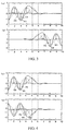
- FIG. 11 shows the convolution result of the equation (1).
- numeral 7 shows input impulse row ( I k or Q k ).
- the upward arrow shows "1" and downward arrow shows "0".
- 8 is an impulse response wave form [ I k ⁇ h ( t- kT ) or Q k ⁇ h ( t-kT ) ] of the LPF for each input impulse 7.
- These impulse response wave forms [ I k ⁇ h ( t- kT ) or Q k ⁇ h ( t-kT ) ] are shown in dotted lines.
- 9 is a filter output wave form [ I (t) or Q (t) ] in which all impulse response wave forms are added.
- the filter output wave form [ I (t) or Q (t) ] is shown in solid line.
- the value of the impulse response becomes negligibly small where
- 5 symbols before and 5 symbols after a certain symbol are used for calculating the convolution of the impulse response.
- the impulse response wave form between the " 5 " symbol and " 6 " symbol shown in the solid line is calculated using 10 symbols shown in FIG. 11.
- the filter output wave form I (t) or Q (t) is obtained as the summation of all impulse response wave forms corresponding to each 10 symbols. That is, the impulse response wave form between the " 5 " symbol and " 6 " is calculated from only 10 symbols of " 1 " to " 10 " symbols.
- FIG. 9 shows a ROM LPF which includes the ROM 24 for storing the wave form described above.
- digital signals I k or Q k (input signal 1 ) are input to the n-step shift register 21.
- the shift register 21 shifts the input data ( symbol ) in sequence and stores the most recent n symbols and outputs these n symbols to the address of the ROM 24.
- n is equal to 10.
- All combination wave forms of n symbols are calculated beforehand and stored in the ROM 24.
- the wave form can not be processed continuously on the time axis. Therefore, the wave forms between two symbols are sampled on the time point of 2 m and the quantized data is stored in the ROM 24.
- the m bits output from the 2 m binary counter 23 which operates at the sampling clock received from the oscillator 22 is input to the ROM 24 as well as the n symbols received from the shift register 21.
- the ROM LPF in FIG. 9 operates as the LPF by selecting the output wave form stored in the ROM 24 at a time according to the address data constructed of n symbol data received from the shift register 21 and by reading in sequence the 2 m sampling number between the two symbols which is selected according to the output value from the counter 23.
- the capacity of the ROM 24 is decided by the referred symbol data n and the sampling number 2 m between the two symbols.
- n becomes larger in order to make the truncation error of the impulse response smaller, the capacity of the ROM will be increasing exponentially.
- FIG. 10 is a block diagram of ROMs LPF 2 i and 2 q configuration which is able to decrease the required capacity of the ROM 24 of FIG. 9.
- the operation of the low pass filter is modified, and expressed by equation (2) which is introduced from the second and third equations of equation (1) as follows.
- equation (2) the range of the impulse response exists between finite n symbols.
- FIG. 12 The filter output wave form is considered as the summation of the filter output wave forms shown in FIGs. 12 (a) and (b). That is, the wave form of the FIG. 12 (a) indicates the first term of the right side of equation ( 2 ) and FIG. 12 (b) indicates the second term of the right side of the equation ( 2 ).
- the reference numbers 71 ⁇ 91 and 72 ⁇ 92 in FIG. 12 correspond to the number 7 ⁇ 9 in FIG. 11.
- the wave forms shown in FIG. 12 (a) and (b) are stored in a ROM 241 and 242 of FIG. 10 respectively in the same way as stored in the ROM 24 in FIG. 9.
- Each n/2 data from the shift registers 211 and 212 and m bit data from the counter 23 are input to the ROMs 241 and 242 respectively , and the corresponding data are read from the ROMs 241 and 242 respectively.
- the two output data from the ROM 241 are added in an adder 25. That is, the ROM 241 operates to calculate the first term of the right side of equation ( 2 ), the ROM 241 operates to calculate the second term of the right side of equation ( 2 ), and the adder 25 calculates the addition of the right side of equation ( 2 ).
- the address data from the shift register 211 is output to the ROM 241, and the address data from the shift register 212 is output to the ROM 242.
- the m bits output from the counter 23 is input to the both ROM 241 and 242. The operation of the m bits output is the same as explained in the FIG. 9.
- the capacity of the ROM of FIG. 10 becomes smaller than that of FIG. 9. But, the capacity of the ROMs 241 and 242 still occupies a considerable amount of memory in the quadrature modulation circuit of FIG. 8. It is also necessary to provide two sets of the same ROM in the quadrature modulation circuit for each I-ch and Q-ch.
- a quadrature modulation circuit includes at least a low pass filter for limiting the frequency band of the in-phase channel and the quadrature channel, along with at least a D/A converter for converting the digital signals received from the low pass filters to analog signals.
- the quadrature modulation circuit also includes at least a filter for suppressing the aliases output from the D/A converters and a quadrature modulator for modulating the outputs from the filters.
- the low pass filters operate by a time division sequence for the in-phase channel and the quadrature channel.
- the low pass filters also use one symbol as a sign data and invert the sign of the remaining symbol data and that of the data read out from the ROM.
- the low pass filters divide the reference data into the first half portion and the second half portion, and read out the contents from the ROM for the forward direction of the time axis at the first half portion, and for the backward direction of the time axis at the second half portion.
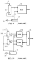
- FIG. 1 shows a first embodiment of the present invention.
- signals 1 i and 1 q are input signals of I-ch and Q-ch respectively.
- a selector 10 switches the input signals 1 i and 1 q to a ROM 20 by a time division process.
- a ROM 20 is a ROM LPF which stores a half of the wave form data using the symmetry characteristic of the wave form data. The adoption of the ROM LPF decreases the capacity of the memory.
- a demultiplexer 11 demultiplexes the output signal from the ROM 20 by a time division process.
- D/A converters 3 i and 3 q convert the input digital signals into analog signals for the I-channel and the Q-channel respectively.
- Analog filters 4 i and 4 q smooth the analog signals, suppress the aliases generated at the sampling process, and output I (t) and Q (t) signals to the quadrature modulator 5 respectively.
- a quadrature modulator 5 modulates the input I (t) and Q (t) signals with the distributed two signals in the same manner as explained in FIG. 8.
- An oscillator 6 supplies the modulation carrier signal to the quadrature modulator 5.
- FIG. 2 shows a block diagram of the selector 10 and the ROM LPF 20 of FIG. 1.
- n/2 step shift registers 211 i , 211 q , 212 i and 212 q shift the input 1 i and 1 q signals in sequence respectively.
- a selector 100 selects one of the outputs from the shift registers 211 i , 211 q , 212 i and 212 q .
- Exclusive ORs 202 and 204 operate so that the amplitude symmetry of the wave form is used for calculating the output signal.
- Exclusive OR 203 operates so that the symmetry of time axis of the wave form is used for calculating the output signal.
- a ROM 201 is addressed by the outputs of the exclusive ORs 202 and 203 and outputs the data to an exclusive OR 204.
- An adder 251 adds the output from the exclusive OR 204.
- a latch circuit 206 latches the output from the adder 251 and uses it for the succeeding addition.
- An oscillator 221 generates a clock signal which is supplied to a counter 231 for counting the clock.
- a timing generator 207 generates the latch clock signal ( CK ) and clear signal ( CLR ) for the latch circuit 206 from the clock signal received from the counter 231.
- signals 1 i and 1 q are input to the selector 10.
- the selector 10 switches the input signals 1 i and 1 q to the ROM LPF 20 by a time division process.
- the ROM LPF 20 stores the filtered wave form data, memory capacity of which is reduced by utilizing the symmetric characteristics of the wave form.
- the same ROM LPF 20 is used both for the in-phase channel and the quadrature channel by a time division process.
- the demultiplexer 11 demultiplexes the output signal from the ROM LPF 20 and sends it to the D/A converters 3 i and 3 q by a time division process.
- Each D/A converter 3 i and 3 q converts the input digital signal into an analog signal.
- Each analog filter 4 i and 4 q smoothes the analog signal, suppresses the aliases generated at the sampling process, and outputs I (t) and Q (t) signals to the quadrature modulator 5 respectively.
- the quadrature modulator 5 modulate a carrier orthogonally with the output signals of the analog filters 4 i and 4 q .
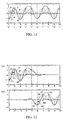
- FIG. 3 shows the symmetrical characteristic of the signal wave form on the time axis.
- Numerals 73 and 74 are input impulse rows respectively
- numerals 83 and 84 are impulse responses for each input impulse.
- Numerals 93 and 94 are output signal wave forms from the filter which are obtained as the summation of all impulse responses 83 and 84 respectively.
- the ROMs 241 and 242 it is necessary to provide the ROMs 241 and 242 for storing the first half n/2 symbols and the second half n/2 symbols respectively. But, the data stored in the ROM 241 is the same as the data stored in the ROM 242 in which the data address is reversely arranged.
- FIG. 3 (b) can be obtained by changing the data sequence from “ 11010 " to " 01011 ", and by reversing the counter number which indicates the sampling position, namely by reversing the time axis and reading out the wave form from the ROM 241.
- the wave forms of FIG. 3 (a) and FIG. 3 (b) can be read out from the same ROM 201 as shown in FIG. 2 .
- FIG. 4 shows the wave form which explains the amplitude symmetry.
- numbers 75 and 76 are inputted impulse sequences respectively
- numbers 85 and 86 are impulse responses for each input impulse.
- Numbers 95 and 96 are the output signal wave forms of the filter which convolutes the impulse responses 85 and 86 respectively.
- the operation for multiplying by ( -1 ) is attained easily by simple hardware. Therefore, the required capacity of the ROM is reduced by half by storing the half wave form in the ROM shown in FIG. 4 (a) , and by multiplying the output wave form by ( -1 ).
- the data on the time axis "5" in FIG. 4 (a) is continuously supervised, and if the data on the time axis "5" is "0", then the data of the time axis "1" ⁇ ”4" are supplied to the ROM 201 as the address data, and if the data on the time axis "5" is "1", then the data of the time axis "1" ⁇ ”4" are inverted and supplied to the ROM 201 as the address data.
- the read out data from the ROM 201 is multiplied by (-1) in the exclusive OR 204.
- FIG. 2 The operation of FIG. 2 is explained hereinafter.
- the first half of the input signal 1 i is stored in the register 211 i and the second half of the signal 1 i is stored in the register 212 i in the same way as described in FIG. 10.
- the first half of the input signal 1 q is stored in the register 211 q and the second half of the signal 1 q is stored in the register 212 q .
- the first n/2 symbols are obtained from the register 211 i and 211 q
- the second n/2 symbols are obtained from the registers 212 i and 212 q .
- a selector 100 selects the input signal from the registers 211 i , 212 q , 212 i and 212 q by the combination of the control signal S 1 and S 0 .
- FIG. 13 shows a time chart which gives wave forms of the signals S 1 , S 0 , latch clock signal CK and clear signal CLR in FIG. 2 and the timing relation between them.
- Latch clock signal CK and the clear signal CLR are generated in the timing generator 207 of FIG. 2.
- the select signal S 1 switches the I channel and Q channels at a sampling point.
- the select signal S 0 switches the first half symbols and the second half symbols of the I channel and the Q channel at a sampling point. That is, the output of the register 211 i is selected when S 1 and S 0 are ( 00 ), and the output of the register 212 i is selected when S 1 and S 0 are ( 01 ). In the same way, the output of the register 211 q is selected when S 1 and S 0 are ( 10 ) and the output of the register 212 q is selected when S 1 and S 0 are ( 11 ).
- the output data selected by the select signal S 1 and S 0 is separated to a specific bit symbol for indicating the sign of the wave form and the remaining ( n/2 -1) bit symbols in order to use the symmetry characteristic of the amplitude of the wave form. These remaining ( n/2 -1) bit symbols are input as the address input to the ROM 201.
- the sign bit is input to the exclusive-OR 202 which inverts the address data. Further, the sign bit is input to an exclusive-OR 204 and an adder 251.
- the output data is processed as two's compliment. Multiplication by (-1) is executed at the exclusive-OR 204 and at the adder 251 by applying " 1 " to the least significant carry bit.
- the impulse response of the first half of the wave form and the impulse response of the second half of the wave form are processed by time division process. Therefore the output of the I channel and Q channel can not be added at a time as shown in FIG. 10.
- the addition in the adder 251 is executed as follows.
- a latch circuit 206 is cleared by the clear pulse CLR received from the timing generator 207 before the first half of the wave form is read out from the ROM 201. After the first half of the wave form has been read from the ROM 201, the latch circuit 206 stores the read out first half of the wave form.
- the second half of the wave form is read out from the ROM 201.
- the output from the adder 251 shows the addition result of the first half and the second half of the wave form.
- the output wave form processed by the ROM LPF is obtained from the adder 251.
- FIG. 5 shows a block diagram of a second embodiment of a quadrature modulation circuit of the present invention.
- a D/A converter 30 is provided which operates by a time division process for I channel and Q channel.
- the output analog signal from the D/A converter 30 is sampled alternately by the sample hold circuits 12 i and 12 q , demultiplexed into the I channel and the Q channel.
- the sample hold circuits 13 i and 13 q operate by the same timing, and align the phase of the I channel and the Q channel.
- FIG. 6 shows a block diagram of a third embodiment of a quadrature modulation circuit of the present invention which is applied to the Gaussian filtered minimum phase shift keying modulation (GMSK).
- GMSK Gaussian filtered minimum phase shift keying modulation
- a signal 101 is inputted to a ROM LPF 20.
- An adder 14 adds the signal from the ROM LPF 20.
- a latch 15 stores the output signal from the adder 14 which is then added to the succeeding output from the ROM LPF 20.
- a COS ROM 16 and a SIN ROM 17 convert the output phase from the adder 14 to I channel signal and Q channel signals respectively.
- input signal 101 is smoothed in the ROM LPF 20.
- the output signal from the ROM LPF 20 is integrated in sequence by the adder 14 and the latch 15, and the signal in the frequency domain is converted into the signal in the phase domain.
- the outputs from the COS ROM 16 and the SIN ROM 17 are converted to analog signals in the D/A converter 3 i , 3 q and supplied to the quadrature modulator 5 through LPF 4 i and 4 q .
- FIG. 7 shows a detailed block diagram of the construction of the ROM LPF 20 of FIG. 6 using amplitude symmetry characteristic.
- numeral 2010 is a ROM
- numeral 2040 is a calculator which multiplies the output from the ROM 2010 by ( -1 ) selectively.
- the same reference number to the FIG. 2 and FIG. 9 is the same portion or the corresponding portion. Accordingly the detailed explanation of the portion is abbreviated in connection with the same number.
- the input signal 101 is stored in a shift register 21.
- One bit of the output signal from the shift register 21 is used as a sign bit and applied to the exclusive-OR 202 and the calculator 2040.
- the sign bit ( 1 bit) and the remaining ( n - 1 ) bits from the shift register 21 are input into the exclusive-OR 202.
- the remaining ( n - 1 ) bits are used as address bits.
- the output signal from the ROM 2010 is multiplied by ( -1 ) in the calculator 2040 when the sign bit is " 1 ". In this manner, the required capacity of the ROM is reduced by half using amplitude symmetry characteristic.
- FIG. 7b shows a detailed block diagram of the construction of the ROM LPF 20 of FIG. 6 using the symmetry on the time axis.
- 1001 is a selector which selects one of the outputs from the shift registers 211,212.
- 2011 is a ROM.
- 2211 is a generator which generates the clock signal.
- 2311 is a counter which counts the clock signal.
- 2071 is a timing generator which generates a latch clock and a clear signal.
- FIG. 7b the same reference numbers as used in FIG. 2 are used to refer to the same portions or corresponding portions. Accordingly the detailed explanation of such portions is omitted in connection with the same reference numbers.
- the input signal 101 is stored in shift registers 211 and 212.
- the first half n/2 symbols of the input signal 101 is stored in the shift register 211 and the second half n/2 symbols of the input signal 101 is stored in the shift register 212.
- the select input signal S 0 selects the first half n/2 symbols or the second half n/2 symbols , that is, the output of the register 211 or 212.
- the selector 1001 selects the second half n/2 symbols from the register 212.
- the output from the register 212 is reversed and the counter data from the counter 2311 is also inverted in the exclusive-OR 203 by the S 0 bit as explained in connection with FIG. 2.
- the impulse responses of the first half wave form and the second half wave form are read from the ROM 2011 by time division process.
- the output data from the ROM 2011 is added in the same way using the adder 251 and the latch 206 as described in connection with FIG. 2.
- the filter output wave form is obtained from the output of the adder 251.
- the required capacity of the ROM is reduced by half using symmetry wave form on the time axis.
Landscapes
- Engineering & Computer Science (AREA)
- Physics & Mathematics (AREA)
- Computer Networks & Wireless Communication (AREA)
- Signal Processing (AREA)
- Nonlinear Science (AREA)
- Spectroscopy & Molecular Physics (AREA)
- Power Engineering (AREA)
- Digital Transmission Methods That Use Modulated Carrier Waves (AREA)
Applications Claiming Priority (4)
| Application Number | Priority Date | Filing Date | Title |
|---|---|---|---|
| JP1264591 | 1991-01-11 | ||
| JP3012645A JP2968350B2 (ja) | 1991-01-11 | 1991-01-11 | 直交変調回路 |
| JP12645/91 | 1991-01-11 | ||
| EP92100452A EP0494696B1 (fr) | 1991-01-11 | 1992-01-13 | Circuit de modulation en quadrature |
Related Parent Applications (2)
| Application Number | Title | Priority Date | Filing Date |
|---|---|---|---|
| EP92100452.9 Division | 1992-01-13 | ||
| EP92100452A Division EP0494696B1 (fr) | 1991-01-11 | 1992-01-13 | Circuit de modulation en quadrature |
Publications (3)
| Publication Number | Publication Date |
|---|---|
| EP0776110A2 true EP0776110A2 (fr) | 1997-05-28 |
| EP0776110A3 EP0776110A3 (fr) | 1997-07-30 |
| EP0776110B1 EP0776110B1 (fr) | 2003-04-16 |
Family
ID=11811105
Family Applications (2)
| Application Number | Title | Priority Date | Filing Date |
|---|---|---|---|
| EP97100128A Expired - Lifetime EP0776110B1 (fr) | 1991-01-11 | 1992-01-13 | Circuit de modulation en quadrature |
| EP92100452A Expired - Lifetime EP0494696B1 (fr) | 1991-01-11 | 1992-01-13 | Circuit de modulation en quadrature |
Family Applications After (1)
| Application Number | Title | Priority Date | Filing Date |
|---|---|---|---|
| EP92100452A Expired - Lifetime EP0494696B1 (fr) | 1991-01-11 | 1992-01-13 | Circuit de modulation en quadrature |
Country Status (5)
| Country | Link |
|---|---|
| US (1) | US5285479A (fr) |
| EP (2) | EP0776110B1 (fr) |
| JP (1) | JP2968350B2 (fr) |
| DE (2) | DE69233017T2 (fr) |
| NO (1) | NO914514L (fr) |
Families Citing this family (31)
| Publication number | Priority date | Publication date | Assignee | Title |
|---|---|---|---|---|
| US5487089A (en) * | 1992-02-17 | 1996-01-23 | Matsushita Electric Industrial Co., Ltd. | Nyquist filter for digital modulation |
| US5420887A (en) * | 1992-03-26 | 1995-05-30 | Pacific Communication Sciences | Programmable digital modulator and methods of modulating digital data |
| US5530722A (en) * | 1992-10-27 | 1996-06-25 | Ericsson Ge Mobile Communications Inc. | Quadrature modulator with integrated distributed RC filters |
| EP0608664B1 (fr) * | 1993-01-29 | 1999-05-06 | STMicroelectronics S.r.l. | Méthode pour filtrer des signaux numériques à haute résolution et architecture correspondante d'un filtre numérique |
| KR0165277B1 (ko) * | 1993-02-27 | 1999-03-20 | 김광호 | 디지탈신호 자기 기록 재생장치 |
| JPH06315039A (ja) * | 1993-04-30 | 1994-11-08 | Toshiba Corp | π/4シフトDQPSK変調器 |
| DE69434132T2 (de) * | 1993-06-25 | 2005-03-17 | Matsushita Electric Industrial Co., Ltd., Kadoma | Verfahren und Einrichtung zur Signalformung von Paketdaten |
| US5541961A (en) * | 1994-08-15 | 1996-07-30 | At&T Corp. | Digitally controlled high resolution hybrid phase synthesizer |
| US5523726A (en) * | 1994-10-13 | 1996-06-04 | Westinghouse Electric Corporation | Digital quadriphase-shift keying modulator |
| US5764693A (en) * | 1994-11-14 | 1998-06-09 | Research In Motion Limited | Wireless radio modem with minimal inter-device RF interference |
| US5619531A (en) * | 1994-11-14 | 1997-04-08 | Research In Motion Limited | Wireless radio modem with minimal interdevice RF interference |
| JP3454623B2 (ja) * | 1995-11-28 | 2003-10-06 | 三洋電機株式会社 | π/4シフトQPSK直交変調装置 |
| US6320914B1 (en) * | 1996-12-18 | 2001-11-20 | Ericsson Inc. | Spectrally efficient modulation using overlapped GMSK |
| KR100237380B1 (ko) * | 1997-06-16 | 2000-01-15 | 이계철 | 고속 롬 기반 나이퀴스트 유한 임펄스 응답 필터 |
| US6459742B1 (en) | 1997-08-04 | 2002-10-01 | Eads Defence And Security Networks | Digital modulation process and modulator implementing the process |
| FR2767002B1 (fr) * | 1997-08-04 | 1999-10-08 | Matra Communication | Procede de modulation numerique, et modulateur mettant en oeuvre un tel procede |
| US6757826B1 (en) | 1998-04-14 | 2004-06-29 | Citicorp Development Center, Inc. | Digital graphic signature system |
| US6359936B1 (en) * | 1998-10-30 | 2002-03-19 | Winbond Electronics Corp. | Modulator employing a memory reduction circuit |
| US7542520B1 (en) | 1999-12-02 | 2009-06-02 | Qualcomm Incorporated | Apparatus and method for implementing a low complexity digital modulator |
| WO2002028126A1 (fr) * | 2000-08-31 | 2002-04-04 | Huawei Technologies Co., Ltd. | Procede de modulation par deplacement de 8 phases (8mdp) et dispositif associe |
| GB2368244A (en) * | 2000-10-10 | 2002-04-24 | Seiko Epson Corp | Signal processor with look-up table for modulating data |
| JP3703083B2 (ja) | 2001-01-10 | 2005-10-05 | 松下電器産業株式会社 | 波形発生装置 |
| US7103108B1 (en) * | 2001-05-17 | 2006-09-05 | Cypress Semiconductor Corp. | Digital signal processor transceiver |
| US7065157B2 (en) * | 2003-03-11 | 2006-06-20 | Qualcomm Inc. | GMSK modulation techniques |
| DE102005053723A1 (de) * | 2005-11-10 | 2007-05-24 | Rohde & Schwarz Gmbh & Co. Kg | Schaltung zur Signalaufbereitung mit gemeinsamen Oszillator |
| US7916808B2 (en) * | 2005-12-23 | 2011-03-29 | Texas Instruments Incorporated | 8PSK modulator |
| EP2612440A4 (fr) | 2010-08-30 | 2014-02-19 | Physical Devices Llc | Dispositifs et procédés de filtrage accordable |
| US9042857B2 (en) | 2010-08-30 | 2015-05-26 | Physical Devices, Llc | Methods, systems, and non-transitory computer readable media for wideband frequency and bandwidth tunable filtering |
| US8520774B1 (en) * | 2010-12-23 | 2013-08-27 | Arris Enterprises, Inc. | Generation of radio frequency outputs |
| EP2820447A4 (fr) | 2012-02-28 | 2015-11-11 | Physical Devices Llc | Procédés, systèmes et supports lisibles par ordinateur pour l'atténuation des interférences dans la bande des signaux du système de positionnement global (gps) |
| US20150244431A1 (en) | 2014-02-21 | 2015-08-27 | Physical Devices, Llc | Devices and methods for diversity signal enhancement and cosite cancellation |
Citations (1)
| Publication number | Priority date | Publication date | Assignee | Title |
|---|---|---|---|---|
| JPS6377246A (ja) | 1986-09-20 | 1988-04-07 | Fujitsu Ltd | デイジタル位相変調回路 |
Family Cites Families (15)
| Publication number | Priority date | Publication date | Assignee | Title |
|---|---|---|---|---|
| US3971996A (en) * | 1973-01-18 | 1976-07-27 | Hycom Incorporated | Phase tracking network |
| NL178640C (nl) * | 1976-07-12 | 1986-04-16 | Philips Nv | Digitale signaalbewerkingsinrichting. |
| DE2913669C2 (de) * | 1979-04-05 | 1981-12-10 | Licentia Patent-Verwaltungs-Gmbh, 6000 Frankfurt | Verfahren zum Erzeugen von Modem-Sendesignalen mit Quadratur-Amplituden-Modulation QAM |
| US4613976A (en) * | 1984-05-02 | 1986-09-23 | British Columbia Telephone Company | Constant envelope offset QPSK modulator |
| JPS60254909A (ja) * | 1984-05-31 | 1985-12-16 | Nippon Precision Saakitsutsu Kk | デイジタルフイルタ |
| NL8402318A (nl) * | 1984-07-23 | 1986-02-17 | Philips Nv | Inrichting voor het genereren van een hoekgemoduleerd draaggolfsignaal van constante amplitude in responsie op datasignalen. |
| DE3579591D1 (de) * | 1984-11-22 | 1990-10-11 | Devon County Council | Daten-modulator-demodulatorsystem. |
| JP2510490B2 (ja) * | 1985-04-10 | 1996-06-26 | 株式会社日立製作所 | デイジタル変調器 |
| JP2595961B2 (ja) * | 1987-04-03 | 1997-04-02 | 日本電気株式会社 | デイジタル変復調システム |
| IE69762B1 (en) * | 1988-11-30 | 1996-10-02 | Motorola Inc | Digital gmsk modulator with non-integer bit interval handling |
| WO1990012451A1 (fr) * | 1989-04-07 | 1990-10-18 | Sharp Kabushiki Kaisha | Modulateur de frequence |
| JPH02295260A (ja) * | 1989-05-10 | 1990-12-06 | Toshiba Corp | 変調器 |
| US4953184A (en) * | 1989-06-01 | 1990-08-28 | Motorola, Inc. | Complex bandpass digital filter |
| US5140613A (en) * | 1990-05-25 | 1992-08-18 | Hewlett-Packard Company | Baseband modulation system with improved ROM-based digital filter |
| KR950003666B1 (ko) * | 1990-12-31 | 1995-04-17 | 삼성전자 주식회사 | 지엠에스케이신호복조방법 및 그 장치 |
-
1991
- 1991-01-11 JP JP3012645A patent/JP2968350B2/ja not_active Expired - Fee Related
- 1991-11-13 US US07/791,228 patent/US5285479A/en not_active Expired - Lifetime
- 1991-11-18 NO NO91914514A patent/NO914514L/no unknown
-
1992
- 1992-01-13 EP EP97100128A patent/EP0776110B1/fr not_active Expired - Lifetime
- 1992-01-13 DE DE69233017T patent/DE69233017T2/de not_active Expired - Fee Related
- 1992-01-13 DE DE69228839T patent/DE69228839T2/de not_active Expired - Fee Related
- 1992-01-13 EP EP92100452A patent/EP0494696B1/fr not_active Expired - Lifetime
Patent Citations (1)
| Publication number | Priority date | Publication date | Assignee | Title |
|---|---|---|---|---|
| JPS6377246A (ja) | 1986-09-20 | 1988-04-07 | Fujitsu Ltd | デイジタル位相変調回路 |
Also Published As
| Publication number | Publication date |
|---|---|
| US5285479A (en) | 1994-02-08 |
| JPH04239245A (ja) | 1992-08-27 |
| DE69233017T2 (de) | 2004-03-25 |
| EP0494696A2 (fr) | 1992-07-15 |
| EP0494696A3 (en) | 1993-05-12 |
| DE69233017D1 (de) | 2003-05-22 |
| DE69228839D1 (de) | 1999-05-12 |
| EP0494696B1 (fr) | 1999-04-07 |
| NO914514D0 (no) | 1991-11-18 |
| EP0776110B1 (fr) | 2003-04-16 |
| JP2968350B2 (ja) | 1999-10-25 |
| EP0776110A3 (fr) | 1997-07-30 |
| NO914514L (no) | 1992-07-13 |
| DE69228839T2 (de) | 1999-11-25 |
Similar Documents
| Publication | Publication Date | Title |
|---|---|---|
| EP0776110B1 (fr) | Circuit de modulation en quadrature | |
| EP0584872B1 (fr) | Modulateur de phase à table de consultation | |
| US5140613A (en) | Baseband modulation system with improved ROM-based digital filter | |
| US5459749A (en) | Multi-level superposed amplitude-modulated baseband signal processor | |
| EP0716785B1 (fr) | Filtre a memoires mortes ameliore | |
| EP0440187A2 (fr) | Dispositif à conversion de signaux binaires d'entrée en signaux en phase et en quadrature correspondants | |
| US5321799A (en) | Signalling transition control in a modulated-signal communications system | |
| US6668013B1 (en) | Digital filter | |
| EP0771097B1 (fr) | Détecteur différentiel pour signaux MDP | |
| US4812786A (en) | Method and system for providing precise multi-function modulation | |
| US6611567B1 (en) | Method and apparatus for pulse shaping | |
| US6278731B1 (en) | Digital transmitter employing digital signal generator utilizing stored waveforms | |
| EP1045561B1 (fr) | Correction de fréquence dans récepteurs multiporteuse | |
| EP0620667A1 (fr) | Modulateur pour signaux pi/4 QPSK | |
| US4631486A (en) | M-phase PSK vector processor demodulator | |
| US6430232B1 (en) | Phase constellation modulator | |
| US6239666B1 (en) | Uniform amplitude modulator | |
| EP0753953B1 (fr) | Procédé et dispositif pour modulation d'amplitude en quadrature à plusieurs niveaux | |
| US6873661B1 (en) | π/4 QPSK modulator | |
| JP3260874B2 (ja) | 1/4πQPSK変調器 | |
| KR100269746B1 (ko) | 디지탈 필터 | |
| JP3260873B2 (ja) | 1/4πQPSK変調器 | |
| KR100192798B1 (ko) | 직각 위상 편이 복조기의 정합 필터 | |
| JPS63215209A (ja) | デジタルフイルタ | |
| JPH06205057A (ja) | 変調器 |
Legal Events
| Date | Code | Title | Description |
|---|---|---|---|
| PUAI | Public reference made under article 153(3) epc to a published international application that has entered the european phase |
Free format text: ORIGINAL CODE: 0009012 |
|
| AC | Divisional application: reference to earlier application |
Ref document number: 494696 Country of ref document: EP |
|
| AK | Designated contracting states |
Kind code of ref document: A2 Designated state(s): DE FR GB SE |
|
| PUAL | Search report despatched |
Free format text: ORIGINAL CODE: 0009013 |
|
| AK | Designated contracting states |
Kind code of ref document: A3 Designated state(s): DE FR GB SE |
|
| 17P | Request for examination filed |
Effective date: 19971029 |
|
| 17Q | First examination report despatched |
Effective date: 20000512 |
|
| GRAH | Despatch of communication of intention to grant a patent |
Free format text: ORIGINAL CODE: EPIDOS IGRA |
|
| GRAH | Despatch of communication of intention to grant a patent |
Free format text: ORIGINAL CODE: EPIDOS IGRA |
|
| GRAA | (expected) grant |
Free format text: ORIGINAL CODE: 0009210 |
|
| AC | Divisional application: reference to earlier application |
Ref document number: 0494696 Country of ref document: EP Kind code of ref document: P |
|
| AK | Designated contracting states |
Designated state(s): DE FR GB SE |
|
| REG | Reference to a national code |
Ref country code: GB Ref legal event code: FG4D |
|
| REF | Corresponds to: |
Ref document number: 69233017 Country of ref document: DE Date of ref document: 20030522 Kind code of ref document: P |
|
| PG25 | Lapsed in a contracting state [announced via postgrant information from national office to epo] |
Ref country code: SE Free format text: LAPSE BECAUSE OF FAILURE TO SUBMIT A TRANSLATION OF THE DESCRIPTION OR TO PAY THE FEE WITHIN THE PRESCRIBED TIME-LIMIT Effective date: 20030716 |
|
| ET | Fr: translation filed | ||
| PLBE | No opposition filed within time limit |
Free format text: ORIGINAL CODE: 0009261 |
|
| STAA | Information on the status of an ep patent application or granted ep patent |
Free format text: STATUS: NO OPPOSITION FILED WITHIN TIME LIMIT |
|
| 26N | No opposition filed |
Effective date: 20040119 |
|
| PGFP | Annual fee paid to national office [announced via postgrant information from national office to epo] |
Ref country code: DE Payment date: 20060105 Year of fee payment: 15 |
|
| PGFP | Annual fee paid to national office [announced via postgrant information from national office to epo] |
Ref country code: FR Payment date: 20060110 Year of fee payment: 15 |
|
| PG25 | Lapsed in a contracting state [announced via postgrant information from national office to epo] |
Ref country code: DE Free format text: LAPSE BECAUSE OF NON-PAYMENT OF DUE FEES Effective date: 20070801 |
|
| GBPC | Gb: european patent ceased through non-payment of renewal fee |
Effective date: 20070113 |
|
| REG | Reference to a national code |
Ref country code: FR Ref legal event code: ST Effective date: 20070930 |
|
| PG25 | Lapsed in a contracting state [announced via postgrant information from national office to epo] |
Ref country code: GB Free format text: LAPSE BECAUSE OF NON-PAYMENT OF DUE FEES Effective date: 20070113 |
|
| PG25 | Lapsed in a contracting state [announced via postgrant information from national office to epo] |
Ref country code: FR Free format text: LAPSE BECAUSE OF NON-PAYMENT OF DUE FEES Effective date: 20070131 |
|
| PGFP | Annual fee paid to national office [announced via postgrant information from national office to epo] |
Ref country code: GB Payment date: 20060111 Year of fee payment: 15 |