EP0777138A2 - Gekrümmter optischer Wellenleiter und Verfahren zu dessen Herstellung - Google Patents
Gekrümmter optischer Wellenleiter und Verfahren zu dessen Herstellung Download PDFInfo
- Publication number
- EP0777138A2 EP0777138A2 EP96308507A EP96308507A EP0777138A2 EP 0777138 A2 EP0777138 A2 EP 0777138A2 EP 96308507 A EP96308507 A EP 96308507A EP 96308507 A EP96308507 A EP 96308507A EP 0777138 A2 EP0777138 A2 EP 0777138A2
- Authority
- EP
- European Patent Office
- Prior art keywords
- optical waveguide
- cladding
- core
- width
- waveguide
- Prior art date
- Legal status (The legal status is an assumption and is not a legal conclusion. Google has not performed a legal analysis and makes no representation as to the accuracy of the status listed.)
- Granted
Links
- 230000003287 optical effect Effects 0.000 title claims abstract description 121
- 238000004519 manufacturing process Methods 0.000 title claims description 23
- 238000005253 cladding Methods 0.000 claims abstract description 80
- 238000000034 method Methods 0.000 claims description 17
- 239000000178 monomer Substances 0.000 claims description 16
- 229920006254 polymer film Polymers 0.000 claims description 7
- 239000000376 reactant Substances 0.000 claims description 5
- 238000001035 drying Methods 0.000 claims description 4
- 230000001678 irradiating effect Effects 0.000 claims description 3
- 238000003780 insertion Methods 0.000 description 14
- 230000037431 insertion Effects 0.000 description 14
- 238000005259 measurement Methods 0.000 description 11
- 239000013307 optical fiber Substances 0.000 description 7
- YMWUJEATGCHHMB-UHFFFAOYSA-N Dichloromethane Chemical compound ClCCl YMWUJEATGCHHMB-UHFFFAOYSA-N 0.000 description 3
- 230000000694 effects Effects 0.000 description 3
- 229920000642 polymer Polymers 0.000 description 3
- VYPSYNLAJGMNEJ-UHFFFAOYSA-N Silicium dioxide Chemical compound O=[Si]=O VYPSYNLAJGMNEJ-UHFFFAOYSA-N 0.000 description 2
- 239000000853 adhesive Substances 0.000 description 2
- 239000011521 glass Substances 0.000 description 2
- 238000001291 vacuum drying Methods 0.000 description 2
- VBHXIMACZBQHPX-UHFFFAOYSA-N 2,2,2-trifluoroethyl prop-2-enoate Chemical compound FC(F)(F)COC(=O)C=C VBHXIMACZBQHPX-UHFFFAOYSA-N 0.000 description 1
- KMNCBSZOIQAUFX-UHFFFAOYSA-N 2-ethoxy-1,2-diphenylethanone Chemical compound C=1C=CC=CC=1C(OCC)C(=O)C1=CC=CC=C1 KMNCBSZOIQAUFX-UHFFFAOYSA-N 0.000 description 1
- SDDLEVPIDBLVHC-UHFFFAOYSA-N Bisphenol Z Chemical compound C1=CC(O)=CC=C1C1(C=2C=CC(O)=CC=2)CCCCC1 SDDLEVPIDBLVHC-UHFFFAOYSA-N 0.000 description 1
- 239000004420 Iupilon Substances 0.000 description 1
- 230000001154 acute effect Effects 0.000 description 1
- 238000005266 casting Methods 0.000 description 1
- 238000010276 construction Methods 0.000 description 1
- 238000005286 illumination Methods 0.000 description 1
- 239000000463 material Substances 0.000 description 1
- 239000011159 matrix material Substances 0.000 description 1
- 239000003504 photosensitizing agent Substances 0.000 description 1
- 239000004431 polycarbonate resin Substances 0.000 description 1
- 229920005668 polycarbonate resin Polymers 0.000 description 1
- 230000001902 propagating effect Effects 0.000 description 1
- 239000011347 resin Substances 0.000 description 1
- 229920005989 resin Polymers 0.000 description 1
- 239000000377 silicon dioxide Substances 0.000 description 1
- 238000000807 solvent casting Methods 0.000 description 1
- 238000005728 strengthening Methods 0.000 description 1
Images


Classifications
-
- G—PHYSICS
- G02—OPTICS
- G02B—OPTICAL ELEMENTS, SYSTEMS OR APPARATUS
- G02B6/00—Light guides; Structural details of arrangements comprising light guides and other optical elements, e.g. couplings
- G02B6/10—Light guides; Structural details of arrangements comprising light guides and other optical elements, e.g. couplings of the optical waveguide type
- G02B6/12—Light guides; Structural details of arrangements comprising light guides and other optical elements, e.g. couplings of the optical waveguide type of the integrated circuit kind
- G02B6/122—Basic optical elements, e.g. light-guiding paths
- G02B6/125—Bends, branchings or intersections
-
- G—PHYSICS
- G02—OPTICS
- G02B—OPTICAL ELEMENTS, SYSTEMS OR APPARATUS
- G02B6/00—Light guides; Structural details of arrangements comprising light guides and other optical elements, e.g. couplings
- G02B6/10—Light guides; Structural details of arrangements comprising light guides and other optical elements, e.g. couplings of the optical waveguide type
- G02B6/12—Light guides; Structural details of arrangements comprising light guides and other optical elements, e.g. couplings of the optical waveguide type of the integrated circuit kind
- G02B2006/12083—Constructional arrangements
- G02B2006/12119—Bend
Definitions
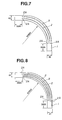
- the range of the point of incidence (range of point A) of the wider optical waveguide can be considered to have shifted in a direction in which the light leakage increases, so that the greater the width of the optical waveguide, the greater the loss.
- waveguides having curved portions inevitably incur loss due to the curvature.
- the degree of loss differs with the waveguide width (D) at the curved portion and the radius (R) of the curvature, depending approximately on the ratio R/D.
- the appropriate range for the waveguide width D is determined among others as a consequence of the core radius of the optical fiber to be connected with this optical waveguide, so that the curvature radius R is important in deciding the shape of the optical waveguide.
- optical waveguides also need to be made as compact as possible to achieve this purpose.
- sharply curved portions greatly increase curvature loss and make it difficult to obtain optical waveguides which satisfy the required performance.
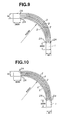
- the optical waveguide relating to the present invention may further comprise a straight portion formed in continuance of said curved portion, wherein the tip of said cladding is formed in the vicinity of the border between such curved portion and the straight portion. Thereby, the light leakage can be reduced further.
- the tip of the cladding may be formed at an arbitrary location in the vicinity of the end of the optical waveguide.
- the present invention also provides a method for manufacturing an optical waveguide, comprising the steps of irradiating a light-transmissive polymer film which contains light reactive monomer via a mask which has an optical waveguide pattern with the cladding according to the above, and thereby reactivating the light reactive monomer of the exposed portion, and drying and removing the non-reactant monomer of the non-exposed portions at said irradiation.
- the insertion loss was greatly improved from 5dB to 2.6dB by providing one cladding.
Landscapes
- Physics & Mathematics (AREA)
- Engineering & Computer Science (AREA)
- Microelectronics & Electronic Packaging (AREA)
- General Physics & Mathematics (AREA)
- Optics & Photonics (AREA)
- Optical Integrated Circuits (AREA)
Applications Claiming Priority (3)
| Application Number | Priority Date | Filing Date | Title |
|---|---|---|---|
| JP30895095 | 1995-11-28 | ||
| JP7308950A JPH09145943A (ja) | 1995-11-28 | 1995-11-28 | 曲がり光導波路およびその製造法 |
| JP308950/95 | 1995-11-28 |
Publications (3)
| Publication Number | Publication Date |
|---|---|
| EP0777138A2 true EP0777138A2 (de) | 1997-06-04 |
| EP0777138A3 EP0777138A3 (de) | 1998-11-11 |
| EP0777138B1 EP0777138B1 (de) | 2002-01-09 |
Family
ID=17987208
Family Applications (1)
| Application Number | Title | Priority Date | Filing Date |
|---|---|---|---|
| EP96308507A Expired - Lifetime EP0777138B1 (de) | 1995-11-28 | 1996-11-25 | Gekrümmter optischer Wellenleiter und Verfahren zu dessen Herstellung |
Country Status (4)
| Country | Link |
|---|---|
| US (1) | US5872883A (de) |
| EP (1) | EP0777138B1 (de) |
| JP (1) | JPH09145943A (de) |
| DE (1) | DE69618434T2 (de) |
Cited By (2)
| Publication number | Priority date | Publication date | Assignee | Title |
|---|---|---|---|---|
| EP1336894A3 (de) * | 2002-02-19 | 2004-12-15 | Omron Corporation | Ein optischer Wellenleiter, ein optisches Bauelement und ein optischer Schalter |
| WO2010116320A1 (en) * | 2009-04-10 | 2010-10-14 | Koninklijke Philips Electronics N.V. | Light guiding bend with curved slits |
Families Citing this family (46)
| Publication number | Priority date | Publication date | Assignee | Title |
|---|---|---|---|---|
| JP4012367B2 (ja) * | 1997-08-04 | 2007-11-21 | インターナショナル・ビジネス・マシーンズ・コーポレーション | 単一モード光ウェーブガイド結合要素 |
| US6370837B1 (en) | 1999-08-04 | 2002-04-16 | Anthony B. Mcmahon | System for laying masonry blocks |
| US6947651B2 (en) * | 2001-05-10 | 2005-09-20 | Georgia Tech Research Corporation | Optical waveguides formed from nano air-gap inter-layer dielectric materials and methods of fabrication thereof |
| US6895133B1 (en) | 2001-06-20 | 2005-05-17 | Lightwave Microsystems Corporation | Crack propagation stops for dicing of planar lightwave circuit devices |
| KR100401203B1 (ko) * | 2001-11-13 | 2003-10-10 | 삼성전자주식회사 | 다항 곡선 광도파로를 구비한 평면 도파로 소자 |
| US20030156819A1 (en) * | 2002-02-15 | 2003-08-21 | Mark Pruss | Optical waveguide |
| JP2003274466A (ja) * | 2002-03-12 | 2003-09-26 | Funai Electric Co Ltd | リモコン受光装置 |
| US7013178B2 (en) * | 2002-09-25 | 2006-03-14 | Medtronic, Inc. | Implantable medical device communication system |
| US20040114875A1 (en) * | 2002-12-17 | 2004-06-17 | Randy Mattsen | 90 Degree fiber optic board connector |
| JP2004287093A (ja) * | 2003-03-20 | 2004-10-14 | Fujitsu Ltd | 光導波路、光デバイスおよび光導波路の製造方法 |
| JP2005010758A (ja) | 2003-05-23 | 2005-01-13 | Sanyo Electric Co Ltd | 光デバイスおよびその製造方法 |
| JP2006337748A (ja) | 2005-06-02 | 2006-12-14 | Fuji Xerox Co Ltd | 光導波路及びその製造方法 |
| JP4965135B2 (ja) * | 2006-02-10 | 2012-07-04 | オムロン株式会社 | 光伝送路、光伝送モジュール、および電子機器 |
| JP4848986B2 (ja) | 2007-03-22 | 2011-12-28 | 富士ゼロックス株式会社 | 光導波路及びその製造方法 |
| JP5278225B2 (ja) * | 2009-07-29 | 2013-09-04 | 住友ベークライト株式会社 | 光導波路、光配線、光電気混載基板および電子機器 |
| WO2011109133A2 (en) * | 2010-03-02 | 2011-09-09 | ExpoImaging, Inc. | Formable photographic device |
| USD632831S1 (en) * | 2010-05-28 | 2011-02-15 | Expolmaging, Inc. | Positionable reflector |
| USD637754S1 (en) * | 2010-05-28 | 2011-05-10 | ExpoImaging, Inc. | Positionable reflector |
| USD637345S1 (en) * | 2010-05-28 | 2011-05-03 | ExpoImaging, Inc. | Flexible multi-positionable rod support for light fixture |
| USD637344S1 (en) * | 2010-05-28 | 2011-05-03 | ExpoImaging, Inc. | Flexible multi-positionable rod support for light fixture |
| USD637346S1 (en) * | 2010-05-28 | 2011-05-03 | ExpoImaging, Inc. | Flexible multi-positionable rod support for light fixture |
| USD633647S1 (en) * | 2010-05-28 | 2011-03-01 | ExpoImaging, Inc. | Positionable reflector |
| JP2012015104A (ja) * | 2010-06-01 | 2012-01-19 | Fujikura Ltd | 面状発光装置 |
| US9442243B2 (en) | 2013-01-30 | 2016-09-13 | Cree, Inc. | Waveguide bodies including redirection features and methods of producing same |
| US9291320B2 (en) | 2013-01-30 | 2016-03-22 | Cree, Inc. | Consolidated troffer |
| US9366396B2 (en) | 2013-01-30 | 2016-06-14 | Cree, Inc. | Optical waveguide and lamp including same |
| US9869432B2 (en) | 2013-01-30 | 2018-01-16 | Cree, Inc. | Luminaires using waveguide bodies and optical elements |
| US10436969B2 (en) | 2013-01-30 | 2019-10-08 | Ideal Industries Lighting Llc | Optical waveguide and luminaire incorporating same |
| US9625638B2 (en) | 2013-03-15 | 2017-04-18 | Cree, Inc. | Optical waveguide body |
| US9690029B2 (en) | 2013-01-30 | 2017-06-27 | Cree, Inc. | Optical waveguides and luminaires incorporating same |
| US10209429B2 (en) | 2013-03-15 | 2019-02-19 | Cree, Inc. | Luminaire with selectable luminous intensity pattern |
| US9366799B2 (en) | 2013-03-15 | 2016-06-14 | Cree, Inc. | Optical waveguide bodies and luminaires utilizing same |
| US9798072B2 (en) | 2013-03-15 | 2017-10-24 | Cree, Inc. | Optical element and method of forming an optical element |
| US10436970B2 (en) | 2013-03-15 | 2019-10-08 | Ideal Industries Lighting Llc | Shaped optical waveguide bodies |
| US10379278B2 (en) * | 2013-03-15 | 2019-08-13 | Ideal Industries Lighting Llc | Outdoor and/or enclosed structure LED luminaire outdoor and/or enclosed structure LED luminaire having outward illumination |
| US9920901B2 (en) | 2013-03-15 | 2018-03-20 | Cree, Inc. | LED lensing arrangement |
| US10400984B2 (en) | 2013-03-15 | 2019-09-03 | Cree, Inc. | LED light fixture and unitary optic member therefor |
| US10502899B2 (en) | 2013-03-15 | 2019-12-10 | Ideal Industries Lighting Llc | Outdoor and/or enclosed structure LED luminaire |
| JP5574001B2 (ja) * | 2013-03-22 | 2014-08-20 | 住友ベークライト株式会社 | 光導波路 |
| US12372219B2 (en) * | 2014-05-30 | 2025-07-29 | Cree Lighting Usa Llc | LED luminaire with a cavity, finned interior, and a curved outer wall extending from a surface on which the light source is mounted |
| US11719882B2 (en) | 2016-05-06 | 2023-08-08 | Ideal Industries Lighting Llc | Waveguide-based light sources with dynamic beam shaping |
| US10416377B2 (en) | 2016-05-06 | 2019-09-17 | Cree, Inc. | Luminaire with controllable light emission |
| WO2020088746A1 (en) * | 2018-10-30 | 2020-05-07 | Telefonaktiebolaget Lm Ericsson (Publ) | Optical add/drop device and assembly, and communications network node |
| WO2021209492A1 (en) * | 2020-04-15 | 2021-10-21 | CommScope Connectivity Belgium BV | Device and method for sealing cables in telecommunications enclosures |
| CN113253450B (zh) * | 2021-05-18 | 2022-06-21 | 浙江大学 | 一种低损耗集成弯曲光波导及其设计方法 |
| US20250355162A1 (en) * | 2022-06-13 | 2025-11-20 | Schott Ag | Thermal expansion-balanced transverse anderson localization optical waveguides that have reduced bowing |
Citations (1)
| Publication number | Priority date | Publication date | Assignee | Title |
|---|---|---|---|---|
| JPS563522B2 (de) | 1976-05-14 | 1981-01-26 |
Family Cites Families (9)
| Publication number | Priority date | Publication date | Assignee | Title |
|---|---|---|---|---|
| DE2041211C3 (de) * | 1970-08-19 | 1973-10-18 | Matth. Hohner Ag, 7218 Trossingen | Vorrichtung zur Beleuchtung einer Fläche mit intensitätsmoduliertem Licht |
| US4472020A (en) * | 1981-01-27 | 1984-09-18 | California Institute Of Technology | Structure for monolithic optical circuits |
| US4824194A (en) * | 1987-03-25 | 1989-04-25 | Fuji Photo Film Co., Ltd. | Light guide apparatus formed from strip light guides |
| US4810049A (en) * | 1987-04-02 | 1989-03-07 | American Telephone And Telegraph Company, At&T Bell Laboratories | Reducing bend and coupling losses in integrated optical waveguides |
| US5292620A (en) * | 1988-01-15 | 1994-03-08 | E. I. Du Pont De Nemours And Company | Optical waveguide devices, elements for making the devices and methods of making the devices and elements |
| EP0365724A1 (de) * | 1988-10-26 | 1990-05-02 | THE GENERAL ELECTRIC COMPANY, p.l.c. | Integrierte optische Wellenleiterkrümmung |
| US5243672A (en) * | 1992-08-04 | 1993-09-07 | At&T Bell Laboratories | Planar waveguide having optimized bend |
| EP0678196B1 (de) * | 1993-01-08 | 2002-04-10 | Massachusetts Institute Of Technology | Verlustarme optische und optoelektronische integrierte schaltungen |
| US5381506A (en) * | 1993-10-18 | 1995-01-10 | Mcdonnell Douglas Corporation | Flat to spiral polymer light waveguide |
-
1995
- 1995-11-28 JP JP7308950A patent/JPH09145943A/ja active Pending
-
1996
- 1996-11-25 US US08/753,433 patent/US5872883A/en not_active Expired - Fee Related
- 1996-11-25 DE DE69618434T patent/DE69618434T2/de not_active Expired - Fee Related
- 1996-11-25 EP EP96308507A patent/EP0777138B1/de not_active Expired - Lifetime
Patent Citations (1)
| Publication number | Priority date | Publication date | Assignee | Title |
|---|---|---|---|---|
| JPS563522B2 (de) | 1976-05-14 | 1981-01-26 |
Cited By (4)
| Publication number | Priority date | Publication date | Assignee | Title |
|---|---|---|---|---|
| EP1336894A3 (de) * | 2002-02-19 | 2004-12-15 | Omron Corporation | Ein optischer Wellenleiter, ein optisches Bauelement und ein optischer Schalter |
| US6950588B2 (en) | 2002-02-19 | 2005-09-27 | Omron Corporation | Optical wave guide, an optical component and an optical switch |
| WO2010116320A1 (en) * | 2009-04-10 | 2010-10-14 | Koninklijke Philips Electronics N.V. | Light guiding bend with curved slits |
| CN102388328A (zh) * | 2009-04-10 | 2012-03-21 | 皇家飞利浦电子股份有限公司 | 具有弯曲狭缝的光导弯曲 |
Also Published As
| Publication number | Publication date |
|---|---|
| DE69618434D1 (de) | 2002-02-14 |
| JPH09145943A (ja) | 1997-06-06 |
| EP0777138B1 (de) | 2002-01-09 |
| EP0777138A3 (de) | 1998-11-11 |
| US5872883A (en) | 1999-02-16 |
| DE69618434T2 (de) | 2002-08-08 |
Similar Documents
| Publication | Publication Date | Title |
|---|---|---|
| EP0777138B1 (de) | Gekrümmter optischer Wellenleiter und Verfahren zu dessen Herstellung | |
| US7289713B2 (en) | Optical waveguide and method of manufacturing the same | |
| EP0428951B1 (de) | Optischer Verteiler für multimodale faseroptische Systeme | |
| CA2028328C (en) | Optical divider for multimode optical fiber systems | |
| EP0598622B1 (de) | Optische Vorrichtung zum Mischen und Verteilen von Licht | |
| EP1810070B1 (de) | Optischer pfad mit einem strahlformer | |
| GB2135075A (en) | Optical waveguide device | |
| KR19990044014A (ko) | 구조면 광 추출 오버레이 및 조명 시스템 | |
| JPH10160961A (ja) | 光学素子 | |
| US6324323B1 (en) | Adhesive-free lens-attached optical fibers to optical waveguide packaging system | |
| EP0785449A1 (de) | Optischer Wellenleiter | |
| EP1757964B1 (de) | Optisches glied mit graduiertem index und optische module damit | |
| JPH09265019A (ja) | 光信号分配装置 | |
| CN114325927A (zh) | 一种用于刻写大模场啁啾光纤光栅的切趾刻写系统 | |
| GB2143650A (en) | Optical coupler | |
| EP0813077A2 (de) | Integrierter, optischer Wellenleiter und Verfahren zur Herstellung | |
| US20110243516A1 (en) | Optical waveguide device, electronic device, and manufacturing method of optical waveguide device | |
| JPS60173508A (ja) | 光導波路接続方法 | |
| US7748910B2 (en) | Optical system and method of manufacturing the same | |
| CN112327419B (zh) | 一种波导垂直光耦合结构 | |
| JPS60175010A (ja) | 光導波路の作製方法 | |
| CN2510887Y (zh) | 挡片式光衰减器 | |
| JPS63282704A (ja) | 光回路の製造方法 | |
| JPH01319707A (ja) | 光合流器 | |
| KR100420958B1 (ko) | 곡면 구조를 갖는 금형의 제조방법 및 이를 이용한광도파로 소자의 제조방법 |
Legal Events
| Date | Code | Title | Description |
|---|---|---|---|
| PUAI | Public reference made under article 153(3) epc to a published international application that has entered the european phase |
Free format text: ORIGINAL CODE: 0009012 |
|
| AK | Designated contracting states |
Kind code of ref document: A2 Designated state(s): DE FR GB |
|
| PUAL | Search report despatched |
Free format text: ORIGINAL CODE: 0009013 |
|
| AK | Designated contracting states |
Kind code of ref document: A3 Designated state(s): DE FR GB |
|
| 17P | Request for examination filed |
Effective date: 19990510 |
|
| 17Q | First examination report despatched |
Effective date: 19991229 |
|
| GRAG | Despatch of communication of intention to grant |
Free format text: ORIGINAL CODE: EPIDOS AGRA |
|
| GRAG | Despatch of communication of intention to grant |
Free format text: ORIGINAL CODE: EPIDOS AGRA |
|
| GRAH | Despatch of communication of intention to grant a patent |
Free format text: ORIGINAL CODE: EPIDOS IGRA |
|
| GRAH | Despatch of communication of intention to grant a patent |
Free format text: ORIGINAL CODE: EPIDOS IGRA |
|
| GRAA | (expected) grant |
Free format text: ORIGINAL CODE: 0009210 |
|
| REG | Reference to a national code |
Ref country code: GB Ref legal event code: IF02 |
|
| AK | Designated contracting states |
Kind code of ref document: B1 Designated state(s): DE FR GB |
|
| REF | Corresponds to: |
Ref document number: 69618434 Country of ref document: DE Date of ref document: 20020214 |
|
| ET | Fr: translation filed | ||
| PGFP | Annual fee paid to national office [announced via postgrant information from national office to epo] |
Ref country code: GB Payment date: 20021030 Year of fee payment: 7 |
|
| PGFP | Annual fee paid to national office [announced via postgrant information from national office to epo] |
Ref country code: FR Payment date: 20021104 Year of fee payment: 7 |
|
| PGFP | Annual fee paid to national office [announced via postgrant information from national office to epo] |
Ref country code: DE Payment date: 20021111 Year of fee payment: 7 |
|
| PLBE | No opposition filed within time limit |
Free format text: ORIGINAL CODE: 0009261 |
|
| STAA | Information on the status of an ep patent application or granted ep patent |
Free format text: STATUS: NO OPPOSITION FILED WITHIN TIME LIMIT |
|
| 26N | No opposition filed | ||
| PG25 | Lapsed in a contracting state [announced via postgrant information from national office to epo] |
Ref country code: GB Free format text: LAPSE BECAUSE OF NON-PAYMENT OF DUE FEES Effective date: 20031125 |
|
| PG25 | Lapsed in a contracting state [announced via postgrant information from national office to epo] |
Ref country code: DE Free format text: LAPSE BECAUSE OF NON-PAYMENT OF DUE FEES Effective date: 20040602 |
|
| GBPC | Gb: european patent ceased through non-payment of renewal fee |
Effective date: 20031125 |
|
| PG25 | Lapsed in a contracting state [announced via postgrant information from national office to epo] |
Ref country code: FR Free format text: LAPSE BECAUSE OF NON-PAYMENT OF DUE FEES Effective date: 20040730 |
|
| REG | Reference to a national code |
Ref country code: FR Ref legal event code: ST |