EP0777207A2 - Verfahren und Vorrichtung zur Schnittstellenbildung zwischen einer Verarbeitungseinheit und Speichern - Google Patents
Verfahren und Vorrichtung zur Schnittstellenbildung zwischen einer Verarbeitungseinheit und Speichern Download PDFInfo
- Publication number
- EP0777207A2 EP0777207A2 EP96307888A EP96307888A EP0777207A2 EP 0777207 A2 EP0777207 A2 EP 0777207A2 EP 96307888 A EP96307888 A EP 96307888A EP 96307888 A EP96307888 A EP 96307888A EP 0777207 A2 EP0777207 A2 EP 0777207A2
- Authority
- EP
- European Patent Office
- Prior art keywords
- memory
- data
- controller
- frame buffer
- out memory
- Prior art date
- Legal status (The legal status is an assumption and is not a legal conclusion. Google has not performed a legal analysis and makes no representation as to the accuracy of the status listed.)
- Withdrawn
Links
Images


Classifications
-
- G—PHYSICS
- G06—COMPUTING OR CALCULATING; COUNTING
- G06T—IMAGE DATA PROCESSING OR GENERATION, IN GENERAL
- G06T1/00—General purpose image data processing
- G06T1/60—Memory management
-
- G—PHYSICS
- G09—EDUCATION; CRYPTOGRAPHY; DISPLAY; ADVERTISING; SEALS
- G09G—ARRANGEMENTS OR CIRCUITS FOR CONTROL OF INDICATING DEVICES USING STATIC MEANS TO PRESENT VARIABLE INFORMATION
- G09G5/00—Control arrangements or circuits for visual indicators common to cathode-ray tube indicators and other visual indicators
- G09G5/36—Control arrangements or circuits for visual indicators common to cathode-ray tube indicators and other visual indicators characterised by the display of a graphic pattern, e.g. using an all-points-addressable [APA] memory
- G09G5/39—Control of the bit-mapped memory
- G09G5/395—Arrangements specially adapted for transferring the contents of the bit-mapped memory to the screen
-
- G—PHYSICS
- G09—EDUCATION; CRYPTOGRAPHY; DISPLAY; ADVERTISING; SEALS
- G09G—ARRANGEMENTS OR CIRCUITS FOR CONTROL OF INDICATING DEVICES USING STATIC MEANS TO PRESENT VARIABLE INFORMATION
- G09G3/00—Control arrangements or circuits, of interest only in connection with visual indicators other than cathode-ray tubes
- G09G3/20—Control arrangements or circuits, of interest only in connection with visual indicators other than cathode-ray tubes for presentation of an assembly of a number of characters, e.g. a page, by composing the assembly by combination of individual elements arranged in a matrix no fixed position being assigned to or needed to be assigned to the individual characters or partial characters
- G09G3/2007—Display of intermediate tones
- G09G3/2018—Display of intermediate tones by time modulation using two or more time intervals
Definitions
- the present invention relates in general to data processing systems and in particular to circuits, systems and methods for interfacing processing circuitry with a memory.
- a typical processing system with video/graphics display capability includes a central processing unit (CPU), a display controller coupled with the CPU by a system bus, a system memory also coupled to the system bus, a frame buffer coupled to the display controller by a local bus, peripheral circuitry (e.g., clock drivers and signal converters), display driver circuitry, and a display unit.
- the CPU generally provides overall system control and, in response to user commands and program instructions retrieved from the system memory, controls the contents of graphics images to be displayed on the display unit.
- the display controller which may for example be a video graphics architecture (VGA) controller, generally interfaces the CPU and the display driver circuitry, exchanges graphics and/or video data with the frame buffer during data processing and display refresh operations, controls frame buffer memory operations, and performs additional processing on the subject graphics or video data, such as color expansion.
- the display driver circuitry converts digital data received from the display controller into the analog levels required by the display unit to generate graphics/video display images.
- the display unit may be any type of device which presents images to the user conveying the information represented by the graphics/video data being processed.
- the frame buffer which is typically constructed from dynamic random access memory devices (DRAMs), stores words of graphics or video data defining the color/gray-shade of each pixel of an entire display frame during processing operations such as filtering or drawing images. During display refresh, this "pixel data" is retrieved out of the frame buffer by the display controller pixel by pixel as the corresponding pixels on the display screen are refreshed.
- the size of the frame buffer directly corresponds to the number of pixels in each display frame and the number of bits (Bytes) in each word used to define each pixel.
- the size and performance of frame buffer is dictated by a number of factors such as, the number of monitor pixels, the monitor DOT clock rate, display refresh, data read/write frequency, and memory bandwidth, to name only a few.
- the frame buffer memory bandwidth is typically constrained by the speed of the memory devices available. For example, a pair of the fastest presently available 256k x 16 DRAMs operating in the page mode can, without interleaving, only provide display refresh data to the display controller at a maximum of rate of 80 to 100 megabytes/second across a 32-bit interface. This limited range accounts not only for the limits on device access time but also for the fact that the frame buffer is simultaneously being burdened with other tasks such as cell refresh, off-screen memory accesses and writes to the on-screen memory. While the available bandwidth may be sufficient for systems driving displays with lower resolutions and/or lower bit depths, it will not support state of the art high resolution/high bit depth displays. For instance, a 1280 by 1024 pixel display with a pixel color depth of 8 bits/pixel being refreshed at 72 hertz requires data from the frame buffer (through the controller) at a rate of at least 130 megabytes/sec.
- Interleaving of the DRAMs (or the random ports of VRAMs when VRAMs are used) of the frame buffer is a memory control/partitioning scheme used in some display systems to improve bandwidth.
- the frame buffer is divided into odd and even banks from which data is alternately retrieved.
- substantial increases in the rate the controller receives data from the memory can be achieved. For example, assume that each bank outputs data at a rate of 40 MHz and the display controller switches between banks at a rate of 80 Mhz, the controller receives a stream of words from the frame buffer at approximately 80 MHz. For a given word width, the bandwidth of the memory is essentially doubled. Interleaving can be similarly extended to memories partitioned more than two banks.
- interleaving provides increased bandwidth
- the complexity of implementing interleaving have limited its application to high end systems.
- the timing and control of the memory becomes a more precise and complicated task for the controller.
- the controller not only must the controller generate additional bank enable signals for switching between banks, but it must also generate the conventional DRAM control signals (RAS, CAS, OE) necessary to retrieve data from each bank at the appropriate times.
- RAS DRAM control signals
- CAS CAS, OE
- circuits, systems and methods for constructing and controlling a memory should allow for the high speed access of data from memory without resort to complex timing schemes required by conventional interleaving techniques. Further, such circuits, systems and methods should be particularly applicable to the control and construction of graphic/video frame buffers.
- the principles of the present invention allow a controller to interface with both on-chip and off-chip memory.
- the on-chip memory provides the controller with fast access storage.
- the off-chip memory allows the controller to interface with a memory which may be substantially larger than that which can be provided on-chip.
- the controller/external memory interface of the present invention allows for the external memory to be expandable.
- the first-in/first-out registers (memories) employed in the novel interface of the present invention eliminate the complex timing schemes required in conventional interleaving schemes.
- a processing system which includes a controller fabricated on an integrated circuit chip along with an internal memory.
- a first first-in/first-out memory is provided having an input for receiving data retrieved from the internal memory and an output for providing data to the controller.
- An external memory is included which interfaces with the controller through a second first-in/first-out memory which has an input for receiving data retrieved from the external memory and an output for providing data to the controller
- a display data processing system which includes an integrated circuit fabricated on a single chip.
- the integrated circuit includes a display controller, an internal frame buffer memory for providing display refresh data at a first predetermined rate through a corresponding data port, and a first first-in/first-out memory interfacing the data port of the internal frame buffer and an input port of the display controller.
- a second first-in/first-out memory is disposed in parallel with the first first-in/first-out memory and includes an output coupled to the input port of the display controller.
- An external frame buffer memory is included for providing display refresh data at a second predetermined rate through a corresponding data port coupled to an input of the second first-in/first-out memory.
- a display system including a display, a frame buffer, controller, and interface circuitry.
- the display is operable to display data as a plurality of pixels on a display screen.
- the frame buffer stores words of pixel data defining characteristics of corresponding pixels on the display screen, the frame buffer including an internal section forming a first part of an integrated controller/frame buffer device and an external portion.
- the controller forms a second part of the integrated controller/frame buffer device and controls the transfer of words of pixel data from the frame buffer to the display.
- the interface circuitry forms a third part of the integrated controller/frame buffer device and includes a first first-in/first-out memory for queuing words of pixel data being transferred from the internal section of the frame buffer to the controller and a second first-in/first-out memory for queuing words of pixel data being transferred from the external section of the frame buffer to the controller.
- first data is received from an internal memory at a first rate at the input of a first first-in/first-out memory.
- Second data is received from an external memory at a second rate at the input of a second first-in/first-out memory.
- a predetermined number of words of the first data are output from the first-in/first-out memory to the controller.
- at least one word of data from the second first-in/first-out memory is output to the controller.
- circuits, systems and methods embodying the principles of the present invention have substantial advantages over the prior art. Among other things, such circuits, systems and methods allow for the high-speed access of data from memory without resort to the complex timing schemes required by conventional interleaving techniques.
- the principles of the present invention are particularly applicable to the control and construction of graphics video frame buffers. In this application, the present invention allows for construction of a large frame buffer which provides data to the controller with substantial bandwidth such that a large displays with high pixel depths can be supported.
- a display control system using a DRAM frame buffer will be used; however, it should be recognized that the principles of the present invention are not limited thereto but may be applied to a number of different processing systems and memory types as will become apparent from the discussion below.
- FIGURE 1 is a high level functional block diagram of the portion of a processing system 100 controlling the display of graphics and/or video data.
- System 100 includes a central processing unit 101, a system bus 102, a display controller 103, a frame buffer 104, a digital to analog converter (DAC) 105 and a display device 106.
- frame buffer 104 includes an internal (on-chip) frame buffer section 104a and an external (off-chip) frame buffer section 104b.
- display controller 103, internal frame buffer 104a and DAC 105 are fabricated together on a single integrated circuit chip 107.
- CPU 101 controls the overall operation of system 100, determines the content of graphics data to be displayed on display unit 106 under user commands, and performs various data processing functions.
- CPU 101 may be for example a general purpose microprocessor used in commercial personal computers.
- CPU 101 communicates with the remainder of system 100 via system bus 102, which may be for example a local bus, an ISA bus or a PCI bus.
- DAC 105 receives digital data from controller 103 and outputs in response the analog data required to drive display 106.
- DAC 105 may also include a color palette, YUV to RGB format conversion circuitry, and/or x- and y-zooming circuitry, to name a few options.
- controller 103 is a display controller, such as a VGA controller, which among other things, controls the exchange of graphics and/or video data with frame buffer 103, controls memory refresh, and performs data processing functions such as color expansion.
- a display controller is the "master" for the specific application of display and thus frees up CPU 101 to perform computational tasks.
- the architecture of a display controller optimizes it to perform graphics and video functions in a manner for superior to that of a general purpose microprocessor.
- Controller 103 may also include a color palette, cursor generation hardware, and/or video to graphics conversion circuitry, to name a few options.
- Frame buffer 104 is preferably a dynamic random access memory (DRAM) which includes an array of rows and columns of DRAM cells and associated address and control circuitry such as row and column decoders, read and write buffers, and sense amplifiers.
- DRAM dynamic random access memory
- Frame buffer 104 may also be constructed from various types of DRAMs including synchronous DRAMs (SDRAMs), cache DRAMs (CDRAMs), MDRAMS, RDRAMs, as well as static RAMs (SRAMs). Frame buffer 104 will be discussed in further detail below.
- Display 106 may be for example a CRT unit or liquid crystal display, electroluminescent display (ELD), plasma display (PLD), or other type of display device displays images on a display screen as a plurality of pixels. Further, display 106 may be a state-of-the-art device such as a digital micromirror device or a silicon carbide like device which directly accepts digital data. It should also be noted that in alternate embodiments, "display" 106 may be another type of output device such as a laser printer or similar document view/print appliances.
- ELD electroluminescent display
- PLD plasma display
- FIGURE 2 depicts a first embodiment of the display refresh interface between display controller 103, internal frame buffer 104a and external frame buffer 104b according to the principles of the present invention (the controller 103/system bus 102 interface is described further below in conjunction with FIGURE 5).
- internal frame buffer 104a and external frame buffer 104b may be different types of DRAMs or alternatively, one may be a DRAM memory of a given type and the other an SRAM memory.
- screen refresh logic 200 of controller 103 receives display data from internal frame buffer 104a through a first-in-first-out memory 201 (FIFO A) and from external frame buffer 104b through first-in-first-out memory 202 and register 203.
- Screen refresh data are "alternatedly" received from FIFOs 201 and 202 and output to display 106 by screen refresh logic 200 during the raster scan of display 106.
- internal frame buffer 104a has a 1 megabyte capacity and is constructed from a pair of parallel 256k by 16 DRAMS 204a and 204b (it should be noted that in alternate embodiments the random ports of video RAMS [VRAMs] may be used).
- VRAMs video RAMS
- the integration of at least part of the frame buffer 104a within the display controller will alone improve bandwidth, notwithstanding the provision of external frame buffer 104b.
- the internal frame buffer 104a will have a substantially improved access speed since, among other things, the capacitive and inductive loading between controller 200 and memory 104a is substantially reduced in the absence of chip to chip interconnections.
- the 16-bit words output from data ports DRAMs 204a and 204b are provided simultaneously in parallel as a 32-bit word to the inputs of FIFO 201. It should be noted that in addition to screen refresh accesses, other accesses are being made to frame buffer 104 while the display screen is being refreshed (e.g., writes to the on-screen space, reads/writes to the off screen space, DRAM cell refreshes, etc.).
- one half a megabyte of external frame buffer 104b is provided as a 256k by 16 DRAM 205. Pairs of 16-bit words output from the data ports of DRAM 205 are received by register 203 and concatenated into 32-bit words which are then provided to the inputs of FIFO B 202.
- the external section 104b allows for the construction of a larger/expandable frame buffer 104 which cannot otherwise be provided by the integrated portion 104a alone.
- the integrated memory 104a is limited in size by the ability to fabricate both memory and controller circuitry on a single yieldable chip.
- the external frame buffer 104b remedies this disadvantage.
- FIFO A 201 for each read made from FIFO B 202.
- the number of reads per FIFO may vary however from application to application.
- the timing of the retrieval of data from internal DRAM 104a and external DRAM 104b is optimized to maintain the data queue in the corresponding FIFO using independent clocks.
- the internal memory 104a and external memory 104b are each controlled by separate DRAM control signals (i.e. RAS, CAS, OE, etc.) Data is then output from FIFOs 201 and 202 respectively at a fixed rate based on the respective input rate.
- RAS DRAM control signals
- the data from FIFOs 201 and 202 preferably directly maps to the screen of display 106. Assuming a pixel depth of 8 bits per pixel, each read of 32-bits from FIFO 201 corresponds to four pixels on the display screen (i.e., one 32-bit "entry" equals four 8-bit pixels). Therefore, the two reads from FIFO 201 will provide data for 8 consecutive pixels in the display raster scan. The following read of one 32-bit word from FIFO 202 provides the data for the next four pixels being generated in the raster scan. The numbers of pixels per word (entry) and the number of corresponding display pixels generated will vary as a function of the pixel depth accordingly.
- the operating parameters for FIFO A and FIFO B in the preferred embodiment can be determined as follows. Initially, assume that only FIFO B (202) is being employed. The calculations will then be extended in the discussion below to the full two FIFO configuration of FIGURE 2.
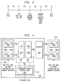
- Single FIFO operation can generally be modeled in accordance with the time line of FIGURE 3.
- FIFO B is assumed to be full with pixel data.
- T 1 it is assumed that substantially half of the data originally in FIFO B at time T 0 has been clocked out for screen refresh. Additionally, at time T 1 , a half-full flag is set.
- other accesses i.e. non-screen refresh operations such as block transfers, graphics data updates, etc. preferably through the controller/bus interface discussed below.
- ⁇ T F X ⁇ T R + Y ⁇ T P
- X is the number of random cycles required
- Y is the number of page mode cycles required
- ⁇ T R is the time required to complete each random cycle
- ⁇ T P is the time required to complete each page mode cycle.
- each FIFO pipeline words or entries, each composed of the pixel data for one or more display pixels.
- ⁇ T 0 is selected to allow an existing DRAM access to complete; normally; ⁇ T 0 would be approximated as the time required to complete one random cycle ( ⁇ T R ) and one page mode cycle ( ⁇ T P ), but can be increased or decreased depending on the demands on the external memory 104b.
- Both ⁇ T 0 and ⁇ T F are defined by other non-screen refresh oriented memory accesses, such as graphics updates and block transfers, etc. It should be recognized that ⁇ T 0 is selected to allow completion of a DRAM access whereas ⁇ T F is set to the length of a complete memory access.
- ⁇ T D represents the time required to unload (clock-out) one entry from the FIFO and thus is dependent on the dot clock rate at which data is retrieved to refresh the display screen.
- ⁇ T D Number of Pixels Per FIFO Entry Dot Clock Rate
- N IFH represents the number of entries left in the FIFO available for screen refresh between time T 1 and time T 3 (i.e. the number of entries remaining after the half-full flag has been set).
- a single FIFO can be modeled as follows, For a fast mode DRAM, page mode cycles ( ⁇ T P ) are typically 40 ns and random cycles ( ⁇ T R ) are typically 140 ns. To set the value of ⁇ T F , it will be assumed that one random cycle and 10 page cycles will be required for other memory operations before the FIFO is half empty from display refresh retrievals. Therefore, ⁇ T F will be 140 + 10 x 40 ns or 540 ns.
- FIFO A and FIFO B both output to an imaginary FIFO at the input of refresh logic 200.
- DRAM bank 204 will output approximately twice as many pixels as DRAM bank 205 since its page mode cycle is approximately twice as fast. From above, ⁇ T D for the imaginary single FIFO is 53.3 nsecs and thus will unload 12 pixels (i.e.
- ⁇ T DA is calculated for FIFO A and ⁇ T DB is the calculation for FIFO B.
- FIGURE 4 depicts an alternate frame buffer interface/partitioning which demonstrates the expandability of the frame buffer 104 according to the principles of the present invention.
- external frame buffer 104b is constructed with two 256k by 16 DRAMs 205a and 205b (1 megabyte of external memory) In this case, 32-bit words are always input to register 205 with each cycle.
- register 205 may be foregone and data transferred directly from external frame buffer 104b to FIFO B 202.
- the embodiment of FIGURE 4 has improved performance (i.e., increased bandwidth) and greater storage capacity. Not only will the embodiment support each of the displays in Table I, but also provides additional space and bandwidth which may be used by controller 103 for the storage of off-screen data.
- FIGURE 5 is a functional block diagram of the display controller 103/system bus 102 interface according to the principles of the present invention.
- Display controller 103 pipelines data to the system bus 102 through conventional BLT engine/CPU access controls 500 during such operations as block transfers and graphics data updates, etc.
- a pair of first-in-first-out memories (registers) 501 and 502 and register 503 queue data to or from internal frame buffer 104a and external memory 104b to BLT engine/controls 500 in a manner discussed above with regards to the display refresh interface.
- FIFOs 501 and 502 can be calculated using the same equations discussed above except that these calculations are based on the timing of the CPU accesses; in this case, the refresh accesses previously discussed become the "other accesses.”
- ⁇ T F now defines the period during which refresh accesses are being made (in contrast, during sizing of refresh FIFOs 201 and 202 ⁇ T F represents the time during which non-screen refresh operations, such as block transfers and graphics data updates, are made).
Landscapes
- Engineering & Computer Science (AREA)
- Physics & Mathematics (AREA)
- General Physics & Mathematics (AREA)
- Theoretical Computer Science (AREA)
- Computer Hardware Design (AREA)
- Controls And Circuits For Display Device (AREA)
- Storage Device Security (AREA)
- Dram (AREA)
- Image Input (AREA)
- Memory System (AREA)
Applications Claiming Priority (2)
| Application Number | Priority Date | Filing Date | Title |
|---|---|---|---|
| US08/552,197 US6108015A (en) | 1995-11-02 | 1995-11-02 | Circuits, systems and methods for interfacing processing circuitry with a memory |
| US552197 | 1995-11-02 |
Publications (2)
| Publication Number | Publication Date |
|---|---|
| EP0777207A2 true EP0777207A2 (de) | 1997-06-04 |
| EP0777207A3 EP0777207A3 (de) | 1998-01-14 |
Family
ID=24204329
Family Applications (1)
| Application Number | Title | Priority Date | Filing Date |
|---|---|---|---|
| EP96307888A Withdrawn EP0777207A3 (de) | 1995-11-02 | 1996-10-31 | Verfahren und Vorrichtung zur Schnittstellenbildung zwischen einer Verarbeitungseinheit und Speichern |
Country Status (4)
| Country | Link |
|---|---|
| US (1) | US6108015A (de) |
| EP (1) | EP0777207A3 (de) |
| JP (1) | JPH09212417A (de) |
| KR (1) | KR100255259B1 (de) |
Cited By (4)
| Publication number | Priority date | Publication date | Assignee | Title |
|---|---|---|---|---|
| WO2000069162A3 (en) * | 1999-05-07 | 2002-01-10 | Intel Corp | A method and apparatus for video decoding |
| EP1628282A1 (de) * | 2004-08-20 | 2006-02-22 | Dialog Semiconductor GmbH | Anzeigesteuerung mit einem grafischen DRAM Speicher |
| WO2007018852A1 (en) * | 2005-07-27 | 2007-02-15 | Sinett Corporation | Queuing and scheduling architecture using both internal and external packet memory for network appliances |
| CN110673816A (zh) * | 2019-10-08 | 2020-01-10 | 深圳市迪太科技有限公司 | 低成本的显存刷新显示屏方法 |
Families Citing this family (12)
| Publication number | Priority date | Publication date | Assignee | Title |
|---|---|---|---|---|
| US6504548B2 (en) | 1998-09-18 | 2003-01-07 | Hitachi, Ltd. | Data processing apparatus having DRAM incorporated therein |
| EP0889478A4 (de) * | 1996-03-21 | 2000-07-19 | Hitachi Ltd | Datenprozessor mit eingebautem dram |
| US6118462A (en) | 1997-07-01 | 2000-09-12 | Memtrax Llc | Computer system controller having internal memory and external memory control |
| JP3359270B2 (ja) * | 1997-10-24 | 2002-12-24 | キヤノン株式会社 | メモリー制御装置と液晶表示装置 |
| US6496869B1 (en) * | 1998-03-26 | 2002-12-17 | National Semiconductor Corporation | Receiving data on a networked computer in a reduced power state |
| US6400361B2 (en) * | 1998-04-23 | 2002-06-04 | United Technologies Dearborn, Inc | Graphics processor architecture employing variable refresh rates |
| JP3786521B2 (ja) * | 1998-07-01 | 2006-06-14 | 株式会社日立製作所 | 半導体集積回路及びデータ処理システム |
| US6329997B1 (en) * | 1998-12-04 | 2001-12-11 | Silicon Motion, Inc. | 3-D graphics chip with embedded DRAM buffers |
| US6704023B1 (en) | 1998-12-04 | 2004-03-09 | Silicon Motion, Inc. | 3-D graphics chip with embedded DRAMbuffers |
| US6820209B1 (en) * | 1999-07-15 | 2004-11-16 | Apple Computer, Inc. | Power managed graphics controller |
| TW476066B (en) * | 1999-11-09 | 2002-02-11 | Winbond Electronics Corp | OSD generation method and structure using dynamic random access memory |
| US7492369B2 (en) | 2004-04-09 | 2009-02-17 | Marvell International Ltd. | Loading an internal frame buffer from an external frame buffer |
Citations (2)
| Publication number | Priority date | Publication date | Assignee | Title |
|---|---|---|---|---|
| EP0660329A2 (de) * | 1993-12-16 | 1995-06-28 | Mosaid Technologies Incorporated | Ausgangpuffer mit variabler Latenz und Synchronisiereinrichtung für synchronen Speicher |
| US5450130A (en) * | 1994-03-30 | 1995-09-12 | Radius Inc. | Method and system for cell based image data compression |
Family Cites Families (25)
| Publication number | Priority date | Publication date | Assignee | Title |
|---|---|---|---|---|
| DE3628286A1 (de) * | 1986-08-20 | 1988-02-25 | Staerk Juergen Dipl Ing Dipl I | Prozessor mit integriertem speicher |
| JPS63245547A (ja) * | 1987-03-31 | 1988-10-12 | Hitachi Ltd | デ−タ処理装置 |
| US4907086A (en) * | 1987-09-04 | 1990-03-06 | Texas Instruments Incorporated | Method and apparatus for overlaying a displayable image with a second image |
| JPH01182992A (ja) * | 1988-01-14 | 1989-07-20 | Mitsubishi Electric Corp | 半導体記憶装置 |
| JPH0283579A (ja) * | 1988-09-21 | 1990-03-23 | Matsushita Electric Ind Co Ltd | 画像データ表示装置と画像データ表示方法 |
| JPH0283578A (ja) * | 1988-09-21 | 1990-03-23 | Matsushita Electric Ind Co Ltd | 画像データ表示装置と画像データ表示方法 |
| EP0429678A4 (en) * | 1989-06-19 | 1992-09-23 | Fujitsu Limited | Dynamic image encoder and dynamic image decoder |
| US5012408A (en) * | 1990-03-15 | 1991-04-30 | Digital Equipment Corporation | Memory array addressing system for computer systems with multiple memory arrays |
| JP3037383B2 (ja) * | 1990-09-03 | 2000-04-24 | キヤノン株式会社 | 画像処理システム及びその方法 |
| US5148272A (en) * | 1991-02-27 | 1992-09-15 | Rca Thomson Licensing Corporation | Apparatus for recombining prioritized video data |
| JP3114228B2 (ja) * | 1991-04-26 | 2000-12-04 | 株式会社日立製作所 | 画像処理装置 |
| US5212742A (en) * | 1991-05-24 | 1993-05-18 | Apple Computer, Inc. | Method and apparatus for encoding/decoding image data |
| JP3158370B2 (ja) * | 1991-07-12 | 2001-04-23 | ソニー株式会社 | ディスクデータ再生装置 |
| JPH05137131A (ja) * | 1991-11-13 | 1993-06-01 | Sony Corp | フレーム間動き予測方法 |
| JP3161614B2 (ja) * | 1991-11-30 | 2001-04-25 | ソニー株式会社 | 動画像復号化装置 |
| US5335322A (en) * | 1992-03-31 | 1994-08-02 | Vlsi Technology, Inc. | Computer display system using system memory in place or dedicated display memory and method therefor |
| US5432900A (en) * | 1992-06-19 | 1995-07-11 | Intel Corporation | Integrated graphics and video computer display system |
| US5408606A (en) * | 1993-01-07 | 1995-04-18 | Evans & Sutherland Computer Corp. | Computer graphics system with parallel processing using a switch structure |
| US5572655A (en) * | 1993-01-12 | 1996-11-05 | Lsi Logic Corporation | High-performance integrated bit-mapped graphics controller |
| DE69420116T2 (de) * | 1993-06-28 | 2000-02-10 | Sony Corp., Tokio/Tokyo | Einrichtung zum dekodieren eines sich zeitlich ändernden bildes |
| US5517612A (en) * | 1993-11-12 | 1996-05-14 | International Business Machines Corporation | Device for scaling real-time image frames in multi-media workstations |
| US5450542A (en) * | 1993-11-30 | 1995-09-12 | Vlsi Technology, Inc. | Bus interface with graphics and system paths for an integrated memory system |
| US5576765A (en) * | 1994-03-17 | 1996-11-19 | International Business Machines, Corporation | Video decoder |
| US5442588A (en) * | 1994-08-16 | 1995-08-15 | Cirrus Logic, Inc. | Circuits and methods for refreshing a dual bank memory |
| US5559999A (en) * | 1994-09-09 | 1996-09-24 | Lsi Logic Corporation | MPEG decoding system including tag list for associating presentation time stamps with encoded data units |
-
1995
- 1995-11-02 US US08/552,197 patent/US6108015A/en not_active Expired - Lifetime
-
1996
- 1996-10-31 EP EP96307888A patent/EP0777207A3/de not_active Withdrawn
- 1996-11-02 KR KR1019960051647A patent/KR100255259B1/ko not_active Expired - Fee Related
- 1996-11-05 JP JP8292717A patent/JPH09212417A/ja active Pending
Patent Citations (2)
| Publication number | Priority date | Publication date | Assignee | Title |
|---|---|---|---|---|
| EP0660329A2 (de) * | 1993-12-16 | 1995-06-28 | Mosaid Technologies Incorporated | Ausgangpuffer mit variabler Latenz und Synchronisiereinrichtung für synchronen Speicher |
| US5450130A (en) * | 1994-03-30 | 1995-09-12 | Radius Inc. | Method and system for cell based image data compression |
Non-Patent Citations (2)
| Title |
|---|
| ALPERT D; AVNON D.: "Architecture of the Pentium Microprocessor", IEEE MICRO, vol. 13, no. 3, June 1993 (1993-06-01), LOS ALAMITOS, CA, USA, pages 11 - 21, XP000380336 * |
| JIANG C.-L.; BOLAN M.: "FIFO - The glue holding systems together", COMPUTER DESIGN, vol. 22, no. 7, June 1983 (1983-06-01), WINCHESTER, MA, USA, pages 181 - 189, XP000743216 * |
Cited By (6)
| Publication number | Priority date | Publication date | Assignee | Title |
|---|---|---|---|---|
| WO2000069162A3 (en) * | 1999-05-07 | 2002-01-10 | Intel Corp | A method and apparatus for video decoding |
| EP1628282A1 (de) * | 2004-08-20 | 2006-02-22 | Dialog Semiconductor GmbH | Anzeigesteuerung mit einem grafischen DRAM Speicher |
| US7446776B2 (en) | 2004-08-20 | 2008-11-04 | Dialog Semiconductor Gmbh | Display controller with DRAM graphic memory |
| WO2007018852A1 (en) * | 2005-07-27 | 2007-02-15 | Sinett Corporation | Queuing and scheduling architecture using both internal and external packet memory for network appliances |
| CN110673816A (zh) * | 2019-10-08 | 2020-01-10 | 深圳市迪太科技有限公司 | 低成本的显存刷新显示屏方法 |
| CN110673816B (zh) * | 2019-10-08 | 2022-09-09 | 深圳市迪太科技有限公司 | 低成本的显存刷新显示屏方法 |
Also Published As
| Publication number | Publication date |
|---|---|
| KR970028997A (ko) | 1997-06-26 |
| JPH09212417A (ja) | 1997-08-15 |
| US6108015A (en) | 2000-08-22 |
| KR100255259B1 (ko) | 2000-05-01 |
| EP0777207A3 (de) | 1998-01-14 |
Similar Documents
| Publication | Publication Date | Title |
|---|---|---|
| US6108015A (en) | Circuits, systems and methods for interfacing processing circuitry with a memory | |
| US5712664A (en) | Shared memory graphics accelerator system | |
| EP0411464A2 (de) | Steuerungsgerät für eine flache Anzeigetafel mit einem Doppelzugriffsspeicher | |
| JPH0420489B2 (de) | ||
| KR100258672B1 (ko) | 다중 뱅크 메모리 아키텍처와 이를 이용한 시스템 및 방법 | |
| US5945974A (en) | Display controller with integrated half frame buffer and systems and methods using the same | |
| US4876663A (en) | Display interface system using buffered VDRAMs and plural shift registers for data rate control between data source and display | |
| EP0563656B1 (de) | Halbleiterspeicheranordnung | |
| EP0166739B1 (de) | Halbleiterspeichervorrichtung für serielle ableseausführungen | |
| EP0700050A2 (de) | Mehrseitenspeicher | |
| JPH11510620A (ja) | 統合されたシステム/フレームバッファメモリ及びシステム、ならびにそれらの使用方法 | |
| US5732024A (en) | Circuits, systems and methods for modifying data stored in a memory using logic operations | |
| JP3001763B2 (ja) | 画像処理システム | |
| US20010040581A1 (en) | Shared memory graphics accelerator system | |
| JPS60251431A (ja) | メモリ表示装置 | |
| KR950001597B1 (ko) | 모니터 리프레쉬(Refresh)를 위한 전용 피포(FIFO)회로 | |
| JPH04274082A (ja) | 半導体記憶装置 | |
| HK1004836A (en) | Display controller with internal half frame buffer and systems and methods using the same | |
| JPH07199907A (ja) | 表示制御装置 | |
| JPH06332791A (ja) | 画像メモリおよびその画像メモリを使用した表示制御システム | |
| EP0847571A1 (de) | Schaltungen und verfahren zur auffrischungssteuerung eines rasterpufferspeichers, der einen sich ausserhalb des schirmes befindenden bereich enthält | |
| HK1002883A (en) | A memory with optimized memory space and wide data input/output and systems and methods using the same | |
| JPH04344385A (ja) | 半導体記憶装置 | |
| JPH02176826A (ja) | 表示制御装置の制御方式 | |
| HK1007912B (en) | Circuits, systems and methods for modifying data stored in a memory using logic operations |
Legal Events
| Date | Code | Title | Description |
|---|---|---|---|
| PUAI | Public reference made under article 153(3) epc to a published international application that has entered the european phase |
Free format text: ORIGINAL CODE: 0009012 |
|
| AK | Designated contracting states |
Kind code of ref document: A2 Designated state(s): BE DE ES FR GB IE IT NL PT |
|
| PUAL | Search report despatched |
Free format text: ORIGINAL CODE: 0009013 |
|
| AK | Designated contracting states |
Kind code of ref document: A3 Designated state(s): BE DE ES FR GB IE IT NL PT |
|
| 17P | Request for examination filed |
Effective date: 19980714 |
|
| 17Q | First examination report despatched |
Effective date: 20010405 |
|
| STAA | Information on the status of an ep patent application or granted ep patent |
Free format text: STATUS: THE APPLICATION IS DEEMED TO BE WITHDRAWN |
|
| 18D | Application deemed to be withdrawn |
Effective date: 20010502 |