EP0777235A2 - Dispositif de mémoire non volatile à semi-conducteur avec une structure de cellule Non-Et - Google Patents
Dispositif de mémoire non volatile à semi-conducteur avec une structure de cellule Non-Et Download PDFInfo
- Publication number
- EP0777235A2 EP0777235A2 EP96118769A EP96118769A EP0777235A2 EP 0777235 A2 EP0777235 A2 EP 0777235A2 EP 96118769 A EP96118769 A EP 96118769A EP 96118769 A EP96118769 A EP 96118769A EP 0777235 A2 EP0777235 A2 EP 0777235A2
- Authority
- EP
- European Patent Office
- Prior art keywords
- memory cell
- gate lines
- control gate
- control
- nand
- Prior art date
- Legal status (The legal status is an assumption and is not a legal conclusion. Google has not performed a legal analysis and makes no representation as to the accuracy of the status listed.)
- Withdrawn
Links
- 239000004065 semiconductor Substances 0.000 title claims abstract description 7
- 238000003491 array Methods 0.000 claims abstract description 33
- 238000009792 diffusion process Methods 0.000 claims abstract description 8
- 239000000758 substrate Substances 0.000 claims abstract description 4
- 239000002131 composite material Substances 0.000 claims description 13
- 230000000295 complement effect Effects 0.000 claims description 4
- 239000002784 hot electron Substances 0.000 claims 1
- 230000000717 retained effect Effects 0.000 claims 1
- 238000010586 diagram Methods 0.000 description 10
- 230000004044 response Effects 0.000 description 4
- 238000002347 injection Methods 0.000 description 2
- 239000007924 injection Substances 0.000 description 2
- 230000007704 transition Effects 0.000 description 2
- 230000005641 tunneling Effects 0.000 description 2
- 230000003213 activating effect Effects 0.000 description 1
- 238000004519 manufacturing process Methods 0.000 description 1
- 230000009467 reduction Effects 0.000 description 1
Images


Classifications
-
- G—PHYSICS
- G11—INFORMATION STORAGE
- G11C—STATIC STORES
- G11C16/00—Erasable programmable read-only memories
- G11C16/02—Erasable programmable read-only memories electrically programmable
- G11C16/06—Auxiliary circuits, e.g. for writing into memory
-
- G—PHYSICS
- G11—INFORMATION STORAGE
- G11C—STATIC STORES
- G11C16/00—Erasable programmable read-only memories
- G11C16/02—Erasable programmable read-only memories electrically programmable
- G11C16/06—Auxiliary circuits, e.g. for writing into memory
- G11C16/10—Programming or data input circuits
- G11C16/14—Circuits for erasing electrically, e.g. erase voltage switching circuits
- G11C16/16—Circuits for erasing electrically, e.g. erase voltage switching circuits for erasing blocks, e.g. arrays, words, groups
-
- G—PHYSICS
- G11—INFORMATION STORAGE
- G11C—STATIC STORES
- G11C16/00—Erasable programmable read-only memories
- G11C16/02—Erasable programmable read-only memories electrically programmable
- G11C16/04—Erasable programmable read-only memories electrically programmable using variable threshold transistors, e.g. FAMOS
- G11C16/0483—Erasable programmable read-only memories electrically programmable using variable threshold transistors, e.g. FAMOS comprising cells having several storage transistors connected in series
Definitions
- the present invention relates to a non-volatile semiconductor memory device and, more particularly to a flash EEPROM (electrically erasable programmable read-only memory) having NAND structure cells with logic circuits for enabling selective erase operation.
- flash EEPROM electrically erasable programmable read-only memory
- a flash EEPROM with NAND structure cells which was originally proposed in F. Masuoka et al "New Ultra High Density EPROM and Flash EEPROM with NAND Structure Cell,” published in the Technical Digest of International Electron Devices Meeting, pp.552-555 (December 1987), is characterized by very small cell area permitting bit density as high as a DRAM. This is due to the reduction in the number of memory cell-to-bit line contacts, thereby to save memory cell area.
- the high bit density and its capability of retaining written data without resorting to backup batteries enable a NAND-structured flash EEPROM to be used as, among others, a stationary replacement for a magnetic disk drive memory system.
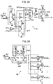
- p-type wells 1 and 2 are formed in the surface of n-type semiconductor substrate 10 in such a manner that they are arranged side by side in the column direction with source line S (to be described later) lying therebetween.
- source line S to be described later
- First memory cell array AR 11 includes eight memory cell transistors M 111 , M 121 , ..., M 181 arranged in the column direction and serially connected with source and drain of every two adjacent cell transistors formed by single n + diffusion region to constitute a first NAND structure having drain of first cell transistor M 111 and source of eighth cell transistor M 181 respectively for connection with first and second select transistors to be described below.
- second memory cell array AR 12 includes eight memory cell transistors M 112 , M 122 , ..., M 182 arranged and mutually serially connected in a manner similar to first memory cell array AR 11 to constitute a second NAND structure having drain of first cell transistor M 112 and source of eighth transistor M 182 respectively for connection with first and second select transistors to be described below.
- the n-th memory cell array AR 1n includes memory cell transistors M 11n , M 12n , ..., M 18n arranged and mutually serially connected in a manner similar to first and second memory cell arrays AR 11 and AR 12 to constitute n-th NAND structure having drain of first cell transistor M 11n and source of eighth cell transistor M 18n respectively for connection with first and second select transistors to be described below.
- Drains of first memory cell transistors M 111 , M 112 , ..., M 11n respectively of the first, second, ..., and n-th memory cell arrays AR 11 , AR 12 , ..., AR 1n serve also as sources of first select transistors T 111 , T 112 , ..., T 11n , respectively, and sources of eighth memory cell transistors M 181 , M 182 , ..., M 18n respectively of the first, second, ..., and n-th memory cell arrays AR 11 , AR 12 , ..., AR 1n serve also as drains of second select transistors T 121 , T 122 , ..., T 12n , respectively.
- Control gates of first cell transistors M 111 , M 112 , ..., M 11n of each of the first to n-th memory cell arrays; control gates of second cell transistors M 121 , M 122 , ..., M 12n of each thereof; ...; and control gates of eighth cell transistors M 181 , M 182 , ..., M 18n of each thereof are connected in common by control gate lines CG 11 , CG 12 , ..., CG 18 , respectively, to form word lines lying in row direction.
- first (drain-side) select transistors T 111 , T 112 , ..., T 11n of the first to n-th memory cell arrays and second (source-side) select transistors T 121 , T 122 , ..., T 12n of the first to n-th memory cell arrays are connected in common by first and second select gate lines SG 11 and SG 12 , respectively.
- first, second, ..., and n-th memory cell arrays AR 21 , AR 22 , ..., AR 2n are formed, with corresponding NAND structure cells and their interconnections arranged in the same manner as those in the first to n-th memory cell arrays AR 11 to AR 1n in p-type well 1, in symmetry with those corresponding thereto with respect to source line S.
- Those corresponding structural elements in p-type well 2 are denoted in Fig. 1 by reference numerals similar to those in p-type well 1 with the most significant digit of the suffix changed from 1 to 2.
- first memory cell array AR 21 in p-type well 2 more specifically for example, memory cell transistors M 211 , M 221 , ..., M 281 are arranged in the order beginning with the furthest end from source line S, to form NAND structure cell, with first (drain-side) select transistor T 211 having source common to drain of first cell transistor M 211 placed at a point furthest from source line S and with second (source-side) select transistor T 221 having drain common to source of eighth cell transistor M 281 placed at a point closest to source line S.
- first (drain-side) select transistor T 211 having source common to drain of first cell transistor M 211 placed at a point furthest from source line S
- second (source-side) select transistor T 221 having drain common to source of eighth cell transistor M 281 placed at a point closest to source line S.
- Control gate lines CG 21 , CG 22 , ..., CG 28 are also formed for these memory cell arrays AR 21 to AR 2n in a manner similar to the corresponding control gate lines CG 11 , CG 12 , ..., CG 18 , symmetrically with the latter with respect to source line S.
- first and second select gate lines SG 21 and SG 22 are formed in a manner similar to those corresponding select gate lines SG 11 and SG 12 , symmetrically with the latter with respect to source line S.
- bit lines B 1 , B 2 , ..., B n are arranged, and connected to the above-mentioned memory cell arrays in such a manner that drains of first select transistors T 111 and T 211 of first memory cell arrays AR 11 and AR 21 in both p-type wells 1 and 2 are connected to bit line B 1 , that drains of first select transistors T 112 and T 212 of second memory arrays AR 12 and AR 22 are connected to bit line B 2 , and drains of first select transistors T 11n and T 21n of n-th memory cell arrays AR 1n and AR 2n are connected to bit line B n .
- Two p-type wells 1 and 2 are connected well lines W 1 and W 2 , respectively. It should be noted in Fig. 1 that memory cell arrays formed in p-type wells 1', 2' adjacently to wells 1 and 2 are not shown for simplicity and clarity.
- Read and write (program) operation for this conventional NAND-structured EEPROM will now be described assuming that memory cell transistor M 122 is to be selected for such operation.
- power supply voltage (5V) is applied to first and second select gate lines SG 11 and SG 12 to turn ON first and second select transistors T 112 and T 122 , while 0 volt is applied to control gate line CG 12 , to which the gate of selected memory cell transistor M 122 is connected, with power supply voltage (5V) applied to other control gate lines than CG 12 (i.e., control gate lines CG 11 , CG 13 , ..., CG 18 ) and with bit line B 2 and source line S set at 1V and 0V, respectively, whereby conductive or non-conductive state of memory cell transistor M 122 is detected for readout of stored data bit.
- first and second select gate lines SG 11 and SG 12 are supplied with high voltage (10V) and 0V, respectively, while control gate lines other than the selected control gate line CG 12 (i.e., control gate lines CG 11 , CG 13 , ..., CG 18 ) are supplied with 10V, with a higher voltage (20V) applied to the selected control gate line CG 12 .
- control gate lines CG 11 , CG 13 , ..., CG 18 are supplied with 10V, with a higher voltage (20V) applied to the selected control gate line CG 12 .
- 0V signifying data bit "0" to be stored is applied to bit line B 2 while intermediate voltage (7V) is applied to all other bit lines.
- the threshold voltage is designed to be lower than the voltage (power supply voltage) applied to non-selected control gate lines (i.e., control gate lines CG 11 , CG 13 , ..., CG 18 in the above example) for read operation but higher than the voltage (0V) applied to the selected control gate line (i.e., control gate line CG 12 ).
- 20V is applied to both first and second select gate lines SG 11 and SG 12 , 0V to all control gate lines CG 11 , CG 12 , ..., CG 18 , and 20V to well line W 1 , while bit lines B 1 to B n and source line S are left in open state.
- a NAND-structured EEPROM described above which utilizes the F-N tunneling for electron injection into floating gate
- Such write operation can be achieved on a word line-by-word line basis (i.e., control gate line-by-control gate line basis) by applying the above-mentioned 0-or 1- representing voltages (0V for "0,” and 7V for "1") respectively to bit lines B 1 to B n and the prescribed voltages to selected and unselected control gate lines as described above.
- NAND structured EEPROM it is not difficult, for a NAND structured EEPROM, to make the unit of simultaneous write operation comparable to that of magnetic storage devices, where the unit of write/erase operation is generally 512 bytes or 1K bytes, often called sector.
- the unit of simultaneous erasure in the NAND-structured EEPROM cannot be easily reduced to that level, because erase operation in the above-described prior art system is performed on a well-by-well basis. It is of course theoretically possible to reduce the size of p-type wells so as to make the unit of simultaneous erasure comparable to that of write operation.
- that approach would seriously reduce bit density of NAND-structured EEPROM, particularly because diffusion margins are required at each side of the regions defining p-type wells due to undesired lateral spread of diffusion involved in manufacturing process.
- Japanese Patent Application Kokai Publication No. Hei 3-290960 entitled “Non-volatile Semiconductor Memory Device” proposes that p-type well having NAND structure cell arrays should be divided into a plurality of erase unit blocks.
- source diffusion layers of select transistors positioned furthest from bit lines i.e., second select transistors T 121 , T 122 , ..., T 12n , T 221 , T 222 , ..., T 22n in the first prior art device described above
- second select transistors T 121 , T 122 , ..., T 12n , T 221 , T 222 , ..., T 22n in the first prior art device described above are made to surround memory cell array regions including desired number of NAND structure cells, thereby to define erasure unit blocks.
- additional wiring forms contact with p-type well.
- the application of a high potential to the above-mentioned source diffusion layer causes depletion layer to be developed to isolate the desired one (selected for erasure) of the memory cell array regions formed in the p-type well, while the erase-causing voltage is applied through the above-mentioned additional wiring of the desired region, thereby limiting the erase operation only to the desired region, i.e., erasure unit block.
- the smallest achievable unit of erasure is reported to be in the order of 4K bytes.
- An object of the invention is to overcome the problems associated with the prior art and to provide flash EEPROM with NAND structure cells having effective means for limiting the area of simultaneous data erasure in such EEPROM to an area comparable to the size corresponding to 512 bytes or 1K bytes of data.
- a flash EEPROM with NAND structure cells having a plurality of memory cell arrays formed in a well of one conductivity type in turn formed in the surface of a semiconductor substrate of opposite conductivity type, each said memory cell arrays being arranged in parallel in column direction and having a plurality of memory cell transistors, source and drain of every two adjacent ones of said memory cell transistors being formed of a single highly doped diffusion region formed in said well, control gates of corresponding ones of said memory cell transistors included respectively in said memory cell arrays being connected respectively to control gate lines lying in parallel in row direction, and first and second ends of each of said NAND structure cells being connected to source and drain respectively of first and second select transistors having control gates connected respectively to first and second select gate lines lying in parallel with said control gate lines, characterized by further comprising logic circuit-based erase control means adapted to control erase operation on control gate line-by-control gate line basis by applying erase control signal of first voltage to those control gate line(s) selected for erasure and that of second voltage to those control gate
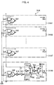
- an erase control circuit 3 is provided, which is arranged in common to all the memory cell arrays AR 11 -AR 1n and AR 21 to AR 2n and to which are connected control gate lines CG 11 -CG 18 and CG 21 -CG 28 .
- Erase control circuit 3 includes subdecoder 31 and main decoder 32, whose circuit diagrams are shown in Figs. 3A and 3B, respectively.
- Fig. 3A shows logic circuits of subdecoder 31 for providing one of decode signals XD 1 to XD 8 corresponding respectively to eight control gate lines CG 11 -CG 18 or CG 21 -CG 28 , which means that subdecoder 31 actually has eight logic circuits identical to the one shown in Fig. 3A.
- Fig. 3B shows logic circuits of main decoder 32 for selectively providing erase control signals to either the eight control gate lines CG 11 -CG 18 of p-type well 1 or the corresponding control gate lines CG 21 -CG 28 of p-type well 2.
- Subdecoder 31 has NAND circuit 311 for providing NAND output n1 of less significant bits LA of row address signal supplied to its input terminals; first clocked inverter circuit 316, to which first control signal LT is applied at the gates of second and third serially connected FETs, directly and through first inverter circuit 314, respectively, and to which NAND output n1 is applied at the gates of first and fourth serially connected FETs; second clocked inverter circuit 317, to which the control signal LT is applied at the gates of third and second FETs, directly and through first inverter 314, respectively, and to which output of clocked inverter circuit 316 from the junction of its second and third FETs is supplied at corresponding junction of second and third FETs thereof; first transfer gate device TG 1 whose gates are supplied with mode switching signal BPG directly and through third inverter 313, respectively, and whose joined drains are supplied with the above-mentioned output from first clocked inverter 316; second transfer gate device TG 2 whose
- Main decoder 32 shown in Fig. 3B has NAND circuit 321 for providing NAND output n 2 of more significant bits UA of row address signal; level shifting circuit 323 whose inputs constituted by gates of FETs Tn 8 and Tn 9 are supplied with the NAND output n 2 directly and through first inverter circuit 322, respectively, and whose load FETs Tp 8 and Tp 9 are supplied with mode switching power supply voltage V px ; and eight transfer gate devices TG 21 , TG 22 , ..., TG 28 , first gate of each thereof being supplied with the output of level shifting circuit 323 and the second gate of each thereof being supplied with the complementary output from level shifting circuit 323.
- each of these transfer gate devices TG 21 to TG 28 are shunted to the ground by FET switch which turns conductive by the complementary output from level shifting circuit 323, so that control gate lines CG 11 to CG 18 may be supplied with the decode outputs XD 1 -XD 8 , respectively, when p-type well 1 is selected by the more significant bits UA of the row address signal or, with ground potential when unselected (another well 2 is selected thereby).
- control gate lines CG 11 and CG 18 are selected for erasure.
- 0V is applied to selected control gate lines CG 11 and CG 18 , while unselected control gate lines CG 12 -CG 17 are set at 20V, equal to the voltage at well line W 1 .
- the application of these voltages results in, as described hereunder, data erasure at those first and eighth cell transistors of each of the memory cell arrays AR 11 to AR 1n , which are controlled by control gate lines CG 11 and CG 18 .
- Each of row addresses of CG 11 and CG 18 supplied from data processing device is divided into less significant bits LA and more significant bits UA.
- NAND output n 1 of LA is latched by first and second clocked inverter circuits 316 and 317 in response to transition of first control signal LT. More specifically, low (L) level of the control signal LT causes NAND output n 1 to be taken in from NAND circuit 311, and its transition to high (H) level causes the signal n 1 to be latched.
- NAND circuit 321 whose NAND output n 2 is supplied to level shifting circuit 323, which results in selection of one of p-type wells 1 and 2 (p-type well 1 in this example) by activating the transfer gate devices TG 21 -TG 28 corresponding to p-type well 1.
- Fig. 4 showing a circuit diagram of another example 31A of subdecoder 31, which characterizes a second embodiment of the present invention
- a section 31A8 thereof corresponding to the control gate line lying furthest from bit line comprises composite circuit 338 consisting of two-input AND gate, three-input AND gate and NOR gate for providing composite logic output; and an inverter 319 for inverting the composite logic output.
- the rest of circuit structure of the section 31A8 is identical to the last and second last stages of subdecoder 31 (Fig. 3A) including inverters 312, 313, 315 and 318, and transfer gate devices TG 1 and TG 2 .
- Three less significant bits LA of row address signal are supplied to the input to the three-input AND gate of composite logic circuit 338, while second control signal ER is applied to one of the inputs to two-input AND gate with the other thereof grounded.
- the output from the inverter circuit 318 of section 31A8 constitutes decode output XD 8
- the output from inverter 319 is supplied as carry signal C to the two-input AND gate of composite logic circuit 337 of the next section 31A7 corresponding to the control gate line lying second furthest from bit line.
- the transfer of carry signal C to next section 31A7 applies to similar transfer of carry signal C from section 31A7 to second next section 31A6, from section 31A6 to third next section 31A5, and so forth.
- the threshold voltage of memory cell transistors needs to be set, for write (program) operation, at a value between 0V and the power supply voltage (5V in this embodiment).
- programming is usually performed in the order of starting with those memory cell transistors lying furthest from bit line-memory cell array contacts and proceeding toward those lying closer thereto. This is because the threshold values of memory cell transistors corresponding to both the outputs "0" and "1" become undistinguishable after the completion of program operation, with the result that the programming voltages (0V or 7V) applied from bit lines when the programming proceeds from those lying closer to the bit line-memory cell array contacts needs to be different.
- control gate lines CG 12 and CG 11 cause erasure in response to address signal corresponding to control gate line CG 12 of p-type well 1.
- the turning to H level of second control signal ER at such erase operation causes the less significant bits LA i (LA 2 in this embodiment) of row address signal to be input as selection signal to the three-input AND gates of composite logic circuits 331-338.
- composite logic circuit 332 outputs a latch signal for itself and provides a carry signal C to composite logic circuit 331 corresponding to the control gate line lying closest to the bit line-memory cell contact. Therefore, the decode output XD 1 of section 31A1 closer to the bit line-memory cell array contact than section 31A2 is provided for selective erasure, together with decode output XD 2 from section 31A2.
- flash EEPROM with NAND structure cells of the present invention makes it possible to perform selective erase operation on control gate line-by-control gate line basis (i.e., word line-by-word line basis) for each p-type well, owing to the provision of erase control means adapted to control the application of erase control voltage consisting of either a voltage equal to the well voltage or a reference voltage, selectively to control gate lines.
- control gate line-by-control gate line basis i.e., word line-by-word line basis
Landscapes
- Engineering & Computer Science (AREA)
- Microelectronics & Electronic Packaging (AREA)
- Read Only Memory (AREA)
- Semiconductor Memories (AREA)
- Non-Volatile Memory (AREA)
Applications Claiming Priority (3)
| Application Number | Priority Date | Filing Date | Title |
|---|---|---|---|
| JP31126095A JP2838993B2 (ja) | 1995-11-29 | 1995-11-29 | 不揮発性半導体記憶装置 |
| JP31126095 | 1995-11-29 | ||
| JP311260/95 | 1995-11-29 |
Publications (2)
| Publication Number | Publication Date |
|---|---|
| EP0777235A2 true EP0777235A2 (fr) | 1997-06-04 |
| EP0777235A3 EP0777235A3 (fr) | 2003-07-16 |
Family
ID=18015007
Family Applications (1)
| Application Number | Title | Priority Date | Filing Date |
|---|---|---|---|
| EP96118769A Withdrawn EP0777235A3 (fr) | 1995-11-29 | 1996-11-22 | Dispositif de mémoire non volatile à semi-conducteur avec une structure de cellule Non-Et |
Country Status (4)
| Country | Link |
|---|---|
| US (1) | US5798547A (fr) |
| EP (1) | EP0777235A3 (fr) |
| JP (1) | JP2838993B2 (fr) |
| KR (1) | KR100246165B1 (fr) |
Cited By (3)
| Publication number | Priority date | Publication date | Assignee | Title |
|---|---|---|---|---|
| WO2000024002A1 (fr) * | 1998-10-20 | 2000-04-27 | Advanced Micro Devices, Inc. | Systeme d'effacement de page et verification d'effacement dans une matrice de memoire remanente |
| EP2135253A4 (fr) * | 2007-03-07 | 2010-04-14 | Mosaid Technologies Inc | Architecture d'effacement de bloc partiel pour mémoire flash |
| US8212304B2 (en) | 2006-03-31 | 2012-07-03 | Semiconductor Energy Laboratory Co., Ltd. | Method for deleting data from NAND type nonvolatile memory |
Families Citing this family (30)
| Publication number | Priority date | Publication date | Assignee | Title |
|---|---|---|---|---|
| KR19990082845A (ko) * | 1998-04-01 | 1999-11-25 | 클라크 3세 존 엠. | 저전압 환경에서 프로그램 가능 및 소거 가능한 단일 폴리 eeprom 셀 및 그 프로그래밍, 소거, 판독 방법 |
| IT1301880B1 (it) * | 1998-07-30 | 2000-07-07 | St Microelectronics Srl | Circuito elettronico di memoria e corrispondente metodo difabbricazione |
| DE69941829D1 (de) * | 1999-04-21 | 2010-01-28 | St Microelectronics Srl | Verfahren zur Herstellung einer nichtflüchtigen Speichervorrichtung |
| JP2001025053A (ja) | 1999-07-09 | 2001-01-26 | Mitsubishi Electric Corp | 携帯電話のメモリシステム |
| US6327183B1 (en) | 2000-01-10 | 2001-12-04 | Advanced Micro Devices, Inc. | Nonlinear stepped programming voltage |
| US6269025B1 (en) | 2000-02-09 | 2001-07-31 | Advanced Micro Devices, Inc. | Memory system having a program and erase voltage modifier |
| US6246610B1 (en) | 2000-02-22 | 2001-06-12 | Advanced Micro Devices, Inc. | Symmetrical program and erase scheme to improve erase time degradation in NAND devices |
| US6304487B1 (en) | 2000-02-28 | 2001-10-16 | Advanced Micro Devices, Inc. | Register driven means to control programming voltages |
| US6295228B1 (en) | 2000-02-28 | 2001-09-25 | Advanced Micro Devices, Inc. | System for programming memory cells |
| US6246611B1 (en) | 2000-02-28 | 2001-06-12 | Advanced Micro Devices, Inc. | System for erasing a memory cell |
| EP1137011B1 (fr) * | 2000-03-21 | 2008-12-10 | STMicroelectronics S.r.l. | Mémoire non-volatile à structure NOR programmable par séquences de mots |
| JP4005761B2 (ja) * | 2000-06-09 | 2007-11-14 | 株式会社東芝 | 半導体記憶装置 |
| CA2320631A1 (fr) * | 2000-09-25 | 2002-03-25 | Pure Technologies Ltd. | Surveillance des cuves et des structures en beton arme |
| US6414873B1 (en) | 2001-03-16 | 2002-07-02 | Simtek Corporation | nvSRAM with multiple non-volatile memory cells for each SRAM memory cell |
| US6512694B2 (en) | 2001-03-16 | 2003-01-28 | Simtek Corporation | NAND stack EEPROM with random programming capability |
| KR100860682B1 (ko) * | 2001-08-20 | 2008-09-26 | 삼성전자주식회사 | 이동 단말기에서 모뎀과 메모리간의 인터페이스장치 및 방법 |
| CA2426183C (fr) * | 2001-08-20 | 2013-02-26 | Samsung Electronics Co., Ltd. | Dispositif et procede permettant d'etablir une interface entre un modem et la memoire d'une station mobile |
| US7332815B2 (en) * | 2003-12-12 | 2008-02-19 | Semiconductor Energy Laboratory Co., Ltd. | Semiconductor device |
| US7170785B2 (en) * | 2004-09-09 | 2007-01-30 | Macronix International Co., Ltd. | Method and apparatus for operating a string of charge trapping memory cells |
| DE102004060375B4 (de) * | 2004-12-15 | 2017-04-06 | Polaris Innovations Ltd. | Doppel-Gate-Speicherzelle und Flash-Speicherchip umfassend eine Anordnung vnon programmirbaren und löschbaren Doppel-Gate-Speicherzellen. |
| JP2007102848A (ja) * | 2005-09-30 | 2007-04-19 | Toshiba Corp | 半導体集積回路装置 |
| KR100725993B1 (ko) * | 2005-12-28 | 2007-06-08 | 삼성전자주식회사 | 누설 전류를 방지하는 로우 디코더 회로 및 이를 구비하는반도체 메모리 장치 |
| KR100749737B1 (ko) * | 2006-01-25 | 2007-08-16 | 삼성전자주식회사 | 노어 플래시 메모리 및 그것의 소거 방법 |
| US7551492B2 (en) * | 2006-03-29 | 2009-06-23 | Mosaid Technologies, Inc. | Non-volatile semiconductor memory with page erase |
| JP2007294082A (ja) * | 2006-03-31 | 2007-11-08 | Semiconductor Energy Lab Co Ltd | Nand型不揮発性メモリのデータ消去方法 |
| US7692973B2 (en) * | 2006-03-31 | 2010-04-06 | Semiconductor Energy Laboratory Co., Ltd | Semiconductor device |
| US20080151654A1 (en) | 2006-12-22 | 2008-06-26 | Allan James D | Method and apparatus to implement a reset function in a non-volatile static random access memory |
| US7940572B2 (en) | 2008-01-07 | 2011-05-10 | Mosaid Technologies Incorporated | NAND flash memory having multiple cell substrates |
| JP2009252255A (ja) | 2008-04-01 | 2009-10-29 | Renesas Technology Corp | 不揮発性半導体記憶装置 |
| US8947122B2 (en) * | 2013-01-14 | 2015-02-03 | Cypress Semiconductor Corporation | Non-volatile latch structures with small area for FPGA |
Family Cites Families (4)
| Publication number | Priority date | Publication date | Assignee | Title |
|---|---|---|---|---|
| JP2862584B2 (ja) * | 1989-08-31 | 1999-03-03 | 株式会社東芝 | 不揮発性半導体メモリ装置 |
| JPH03290960A (ja) * | 1990-03-30 | 1991-12-20 | Toshiba Corp | 不揮発性半導体記憶装置 |
| JP3099887B2 (ja) * | 1990-04-12 | 2000-10-16 | 株式会社東芝 | 不揮発性半導体記憶装置 |
| US5197027A (en) * | 1991-01-24 | 1993-03-23 | Nexcom Technology, Inc. | Single transistor eeprom architecture |
-
1995
- 1995-11-29 JP JP31126095A patent/JP2838993B2/ja not_active Expired - Fee Related
-
1996
- 1996-11-13 US US08/748,278 patent/US5798547A/en not_active Expired - Lifetime
- 1996-11-22 EP EP96118769A patent/EP0777235A3/fr not_active Withdrawn
- 1996-11-29 KR KR1019960059400A patent/KR100246165B1/ko not_active Expired - Fee Related
Non-Patent Citations (1)
| Title |
|---|
| "Technical Digest of International Electron Devices Meeting.", December 1987, article MASUOKA F. ET AL.: "New Ultra High Density EPROM and Flash EEPROM with NAND Structure Cell.", pages: 552 - 555, XP000091991 |
Cited By (5)
| Publication number | Priority date | Publication date | Assignee | Title |
|---|---|---|---|---|
| WO2000024002A1 (fr) * | 1998-10-20 | 2000-04-27 | Advanced Micro Devices, Inc. | Systeme d'effacement de page et verification d'effacement dans une matrice de memoire remanente |
| US8212304B2 (en) | 2006-03-31 | 2012-07-03 | Semiconductor Energy Laboratory Co., Ltd. | Method for deleting data from NAND type nonvolatile memory |
| EP2135253A4 (fr) * | 2007-03-07 | 2010-04-14 | Mosaid Technologies Inc | Architecture d'effacement de bloc partiel pour mémoire flash |
| US7804718B2 (en) | 2007-03-07 | 2010-09-28 | Mosaid Technologies Incorporated | Partial block erase architecture for flash memory |
| US8842472B2 (en) | 2007-03-07 | 2014-09-23 | Conversant Intellectual Property Management Inc. | Partial block erase architecture for flash memory |
Also Published As
| Publication number | Publication date |
|---|---|
| KR970029865A (ko) | 1997-06-26 |
| JP2838993B2 (ja) | 1998-12-16 |
| EP0777235A3 (fr) | 2003-07-16 |
| KR100246165B1 (ko) | 2000-03-15 |
| JPH09153292A (ja) | 1997-06-10 |
| US5798547A (en) | 1998-08-25 |
Similar Documents
| Publication | Publication Date | Title |
|---|---|---|
| US5798547A (en) | Non-volatile semiconductor memory device having NAND structure cells | |
| EP0525678B1 (fr) | Mémoire à semi-conducteurs permanent ayant un décodeur pour lignes | |
| CA1185369A (fr) | Memoire morte programmable effacable electriquement | |
| US5313432A (en) | Segmented, multiple-decoder memory array and method for programming a memory array | |
| US5740107A (en) | Nonvolatile integrated circuit memories having separate read/write paths | |
| US5109361A (en) | Electrically page erasable and programmable read only memory | |
| US5245570A (en) | Floating gate non-volatile memory blocks and select transistors | |
| US5646886A (en) | Flash memory having segmented array for improved operation | |
| US5369609A (en) | Floating gate memory array with latches having improved immunity to write disturbance, and with storage latches | |
| KR970003095B1 (ko) | 메모리 셀 트랜지스터를 과잉 소거 상태로 되게 하는 기능을 구비한 비휘발성 반도체 메모리 장치와 그 장치에서의 데이타 기록 방법 | |
| US8120955B2 (en) | Array and control method for flash based FPGA cell | |
| US4543647A (en) | Electrically programmable non-volatile semiconductor memory device | |
| US5287536A (en) | Nonvolatile memory array wordline driver circuit with voltage translator circuit | |
| EP0586473A4 (fr) | ||
| EP1345235A1 (fr) | Commutateur programmable non volatile bidirectionnel pour logique programmable | |
| KR960005370B1 (ko) | 비휘발성 반도체 메모리 장치를 소거하고 검증하기 위한 방법 및 장치 | |
| JP2002352591A (ja) | 不揮発性半導体メモリ装置、そのローカルロウデコーダ構造、及び半導体メモリ装置、同装置でのワードライン駆動方法 | |
| CN1897160B (zh) | 包含存储单元与限流器的半导体元件 | |
| US5105386A (en) | Nonvolatile semiconductor memory device with reduced variation in source potential of floating gate type memory transistors and operating method therefor | |
| US5422846A (en) | Nonvolatile memory having overerase protection | |
| US6775186B1 (en) | Low voltage sensing circuit for non-volatile memory device | |
| US5197029A (en) | Common-line connection for integrated memory array | |
| EP1274091B1 (fr) | Mémoire nonvolatile à semiconducteurs avec une architecture de blocs et une charge minimisée du générateur interne de tension | |
| KR20010013737A (ko) | 비휘발성 반도체 저장 장치용 구동 회로 | |
| KR100274750B1 (ko) | 비휘발성반도체기억장치의구동방법 |
Legal Events
| Date | Code | Title | Description |
|---|---|---|---|
| PUAI | Public reference made under article 153(3) epc to a published international application that has entered the european phase |
Free format text: ORIGINAL CODE: 0009012 |
|
| AK | Designated contracting states |
Kind code of ref document: A2 Designated state(s): DE FR IT |
|
| RAP1 | Party data changed (applicant data changed or rights of an application transferred) |
Owner name: NEC ELECTRONICS CORPORATION |
|
| PUAL | Search report despatched |
Free format text: ORIGINAL CODE: 0009013 |
|
| AK | Designated contracting states |
Designated state(s): DE FR IT |
|
| RIC1 | Information provided on ipc code assigned before grant |
Ipc: 7G 11C 16/14 B Ipc: 7G 11C 16/04 B Ipc: 7G 11C 16/06 A |
|
| 17P | Request for examination filed |
Effective date: 20030611 |
|
| 17Q | First examination report despatched |
Effective date: 20031024 |
|
| STAA | Information on the status of an ep patent application or granted ep patent |
Free format text: STATUS: THE APPLICATION IS DEEMED TO BE WITHDRAWN |
|
| 18D | Application deemed to be withdrawn |
Effective date: 20040504 |