EP0777239A1 - Gehäuseanordnung zur vergossenen Aufnahme einer elektronischen Baueinheit - Google Patents
Gehäuseanordnung zur vergossenen Aufnahme einer elektronischen Baueinheit Download PDFInfo
- Publication number
- EP0777239A1 EP0777239A1 EP95118991A EP95118991A EP0777239A1 EP 0777239 A1 EP0777239 A1 EP 0777239A1 EP 95118991 A EP95118991 A EP 95118991A EP 95118991 A EP95118991 A EP 95118991A EP 0777239 A1 EP0777239 A1 EP 0777239A1
- Authority
- EP
- European Patent Office
- Prior art keywords
- housing
- chamber
- housing arrangement
- arrangement according
- opening
- Prior art date
- Legal status (The legal status is an assumption and is not a legal conclusion. Google has not performed a legal analysis and makes no representation as to the accuracy of the status listed.)
- Granted
Links
Images



Classifications
-
- H—ELECTRICITY
- H01—ELECTRIC ELEMENTS
- H01F—MAGNETS; INDUCTANCES; TRANSFORMERS; SELECTION OF MATERIALS FOR THEIR MAGNETIC PROPERTIES
- H01F27/00—Details of transformers or inductances, in general
- H01F27/40—Structural association with built-in electric component, e.g. fuse
- H01F27/402—Association of measuring or protective means
-
- H—ELECTRICITY
- H01—ELECTRIC ELEMENTS
- H01F—MAGNETS; INDUCTANCES; TRANSFORMERS; SELECTION OF MATERIALS FOR THEIR MAGNETIC PROPERTIES
- H01F27/00—Details of transformers or inductances, in general
- H01F27/02—Casings
- H01F27/022—Encapsulation
-
- H—ELECTRICITY
- H01—ELECTRIC ELEMENTS
- H01F—MAGNETS; INDUCTANCES; TRANSFORMERS; SELECTION OF MATERIALS FOR THEIR MAGNETIC PROPERTIES
- H01F27/00—Details of transformers or inductances, in general
- H01F27/40—Structural association with built-in electric component, e.g. fuse
- H01F27/402—Association of measuring or protective means
- H01F27/406—Temperature sensor or protection
Definitions
- the invention relates to a housing arrangement for potting an electronic component, in particular a transformer, which is connected to a protective element against overcurrent.
- PTC elements As a protective element against overcurrent is known.
- the PTC element is cast together with the structural unit in a casting compound, for example made of epoxy resin.
- the potting compound increases the heat dissipation from the electronic unit, so that larger powers can be switched, or the unit can be made smaller.
- the potting of the protective element leads to the fact that the customer of the structural unit does not circumvent the safety requirements, since the protective element is firmly connected to it.
- a selective heating of the casting compound also leads to an accelerated aging of the casting compound. Voltage flashovers can occur in the area of the PTC resistor. If an arc forms, the risk of fire is also very high.
- the object of the invention is to provide a variant when using the known encapsulation technique, which ensures the safe functioning of the protective element.
- the invention solves this problem in a housing arrangement of the type mentioned above by a separate chamber for receiving the protective element.
- the protective element Since the protective element is in a separate chamber, it is not in direct contact with the sealing compound. In particular, it does not come into contact with the hot casting compound during the manufacturing process. If the casting compound cools down, mechanical stresses can only occur on the walls of the chamber, since only these are in contact with the casting compound. If the protective element is a PTC resistor, the chamber can effectively prevent the mechanical stresses from damaging the doped ceramic body of the PTC resistor when the casting compound cools.
- a selective heating of the potting compound is prevented, since the protective element only transfers heat to the potting compound via a heat-insulating air layer in the chamber.
- the protective element therefore remains functional until the external power supply is interrupted by switching off.
- the chamber for the protective element is contained separately in the housing arrangement, so that the invention further ensures that a consumer of the electronic unit meets the safety requirements e.g. cannot handle for cost reasons.
- the chamber has an opening lying on an outside of the encapsulated housing arrangement.
- the chamber is accessible at all times through the opening on the outside of the housing arrangement, so that the protective element can be installed both before and after the unit has been cast. Furthermore, the protective element can be checked from the outside during or after operation of the electronic unit and replaced if necessary.
- This closure element can be a hinged lid connected to a side wall of the housing arrangement or a lid that can be fitted onto the chamber, preferably in a snug fit.
- a cost-effective variant is that the opening is fastened to the housing arrangement in such a way that when the housing arrangement is mounted on a carrier, for example a printed circuit board, the opening is closed by the carrier.
- An embodiment of the invention is that the chamber is arranged in a housing accommodating the structural unit. Since the external dimensions of the housing are standardized and the customers have adjusted to these dimensions, arranging the chamber within the housing ensures that the external dimensions of the housing do not change and therefore the customers do not have to change the design of their devices.
- the chamber is integrally formed on the housing. This measure enables the chamber to be produced simultaneously with the housing, so that the chamber only incurs low additional production costs.
- the chamber can also be manufactured as an individual part and is connected to the housing or the structural unit in a later work step by measures known to the person skilled in the art. These measures include gluing, screwing, riveting, etc.
- the connection of the chamber is made particularly easy by the use of latching elements, in particular push buttons and clips.
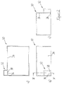
- Figures 1a, 1b and 1c show a first housing 10 in a bottom, front and side view. The bottom view is shown in Figure 1a.
- a chamber 12 is integrally formed on the left housing wall 14 in the interior of the housing 10.
- a recess 16 in a wall 18 of the chamber 12 enables an electrical line (see FIG. 3) to be laid between the interior of the chamber 12 and the interior of the housing 10.
- FIG. 1b The front view of the housing 10 is shown under the bottom view in FIG. 1b.
- a further recess 20 in the chamber 12 enables the laying of a further line (cf. FIG. 3) between the chamber 12 and the interior of the housing 10.
- Figure 1c shows a side view of the housing 10. The expansion of the chamber 12 in its The longitudinal direction and its height, as well as its position in the housing 10 are clear in Figure 1c.
- FIG. 2a Figures 2a, b and c show a second housing 30 in a bottom, front and side view.
- the bottom view of the housing 30 is shown in FIG. 2a.
- a chamber 32 is integrally formed on a wall 34 outside the housing 30.
- Two cutouts 36 and 38 in the housing wall 34 serve to receive electrical lines (see FIG. 4) between the chamber 32 and the interior of the housing 30.
- FIG. 2b shows a side view of the housing 30, which makes the position of the chamber 32 with respect to the housing 30 clear.
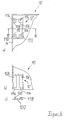
- FIG 3 shows the housing 10 as section III-III of Figure 1b.
- the interior of the housing 10 is filled with a potting compound 50.
- the walls of the chamber 12 keep the potting compound 50 from a PTC resistor 52.
- Leads 54 and 56 of the PTC resistor are connected via connecting points 58 and 60 to lines 42 and 44 to form an electronic component contained in the interior of the casting compound 30.
- the line 62 or 64 runs through the cutouts 16 or 20.
- FIG 4 shows the housing 30 as section IV-IV corresponding to Figure 2b.
- the interior of the housing 30, which also contains a transformer, not shown, is filled with the potting compound 70.
- the housing wall 34 keeps the potting compound 50 from a PTC resistor 72 in the interior of the chamber 32.
- a feed line 74 is connected via a connection point 76 to a line 78 which runs through the recess 36 from the chamber 32 into the interior of the housing 30.
- the line 78 and a further line, not shown, connect the PTC resistor 72 to the transformer cast in the sealing compound 70.
- FIGS. 5a, b and c show a first embodiment of a closure of a chamber 12 'formed on the housing 10 instead of the chamber 12 with a closure cover 90.
- the chamber 12' has reinforced walls.
- a groove 96 is located between an inner wall 92 and an outer wall 94 of the chamber 12 '.
- Figure 5b shows the section V-V of the chamber 12 'of Figure 5a.
- the depth of the groove 96 can be seen in FIG. 5b. It corresponds to the height of the closure cap 90 in accordance with FIG. 5c.
- the closure cover 90 is designed such that it is pressed into the groove 96 under pressure. Due to a snug fit there is a non-positive connection between the closure cover 90 and chamber 12 '.
- the chamber 12 ' can be closed after the PTC resistor 52 has been inserted, so that the PTC resistor is protected against environmental influences and unwanted contact.
- FIGS. 6a, b and c show a second embodiment of a closure of a chamber 12 ′′ formed on the housing 10 instead of the chamber 12, with a closure cover 100.
- a molded-on shaped element 102 to 108 for receiving one axial bore 110 to 116 each.
- Figure 6b shows the section VI-VI of the chamber 12 '' of Figure 6a.
- 6b shows the depth of the bores 114 and 116, which also corresponds to the depth of the bores 110 and 112.
- the opening of the chamber 12 '' is chamfered.
- the closure lid 100 shown in FIG. 6c is also beveled in its edge areas, so that it can optimally close the chamber 12 ′′.
- the length of the pins 118 and 120 and their diameter correspond to the diameter and the length of the associated bores 114 and 116 roughly match.
- the chamber 12 ′′ is closed by inserting the closure cover 100 under pressure into the opening of the chamber 12 ′′. Due to a snug fit, the closure cap 100 is held in place by the chamber 12 ′′. This means that the chamber 12 '' can be securely closed and opened at any time.
Landscapes
- Engineering & Computer Science (AREA)
- Power Engineering (AREA)
- Details Of Resistors (AREA)
- Casings For Electric Apparatus (AREA)
- Coils Or Transformers For Communication (AREA)
- Dc-Dc Converters (AREA)
- Housings And Mounting Of Transformers (AREA)
- Transformers For Measuring Instruments (AREA)
Abstract
Description
- Die Erfindung betrifft eine Gehäuseanordnung zur vergossenen Aufnahme einer elektronischen Baueinheit, insbesondere eines Transformators, die mit einem Schutzelement gegen Überstrom verbunden ist.
- Für elektronische Baueinheiten, insbesondere Transformatoren, müssen Sicherheitsanforderungen hinsichtlich Überstrom eingehalten werden. Diese Sicherheitsanforderungen sollen Umgebungsschäden verhüten, wenn durch einen Windungs- oder Kurzschluß eine übermäßige Strombelastung auftritt, welche zu Brandschäden an der Baueinheit und in der Umgebung führen kann. Bekannt ist der Einsatz von PTC-Elementen als Schutzelement gegen Überstrom. Insbesondere wird das PTC-Element gemeinsam mit der Baueinheit in einer Vergußmasse, z.B. aus Epoxidharz, vergossen. Die Vergußmasse erhöht dabei die Wärmeableitung von der elektronischen Baueinheit, so daß größere Leistungen geschaltet werden können, bzw. die Baueinheit kleiner ausgeführt werden kann. Das Mitvergießen des Schutzelementes führt dazu, daß der Abnehmer der Baueinheit die Sicherheitsanforderungen nicht umgeht, da das Schutzelement fest mit ihr verbunden ist.
- Durch das Vergießen eines Schutzelementes und insbesondere eines PTC-Widerstandes entstehen neue Sicherheitsrisiken. Die bisherige Vergußtechnik sieht keine Maßnahmen vor, um ein Beschädigen des Schutzelementes durch die warme Vergußmasse beim Herstellungsverfahren zu vermeiden. Beim Abkühlen der Vergußmasse kommt es zu Spannungen, die sich auch auf das Schutzelement übertragen und zu dessen Beschädigung führen können, indem feine Haarrisse am Schutzelement entstehen.
- Ein beschädigtes Schutzelement hat zur Folge, daß der Schutz der elektronischen Baueinheit im Falle eines Überstroms versagt. Die Folge ist eine übermäßige Erhitzung der elektronischen Baueinheit, die zu Bränden führen kann.
- Bei einer übermäßigen Strombelastung fließt durch den PTC-Widerstand ein Ruhestrom, wodurch sich der PTC-Widerstand bis auf 180°C erwärmen kann. Die Folge ist ein punktuelles Erhitzen der Vergußmasse. Befinden sich z.B. mit Isolierlack versehene Drähte eines Transformators in der Nähe der erhitzten Vergußmasse, so kann die Isolierung beschädigt werden, wodurch die elektrische Baueinheit weiter beschädigt wird, womit der Schaden durch das Schutzelement nicht begrenzt, sondern vergrößert wird.
- Ein punktuelles Erhitzen der Vergußmasse führt weiterhin zu einem beschleunigten Altern der Vergußmasse. Es kann zu Spannungsüberschlägen im Bereich des PTC-Widerstandes kommen. Bildet sich ein Lichtbogen, so ist die Brandgefahr ebenfalls sehr hoch.
- Aufgabe der Erfindung ist es, bei Verwenden der bekannten Vergußtechnik eine Variante anzugeben, die ein sicheres Funktionieren des Schutzelementes gewährleistet.
- Die Erfindung löst diese Aufgabe bei einer Gehäuseanordnung eingangs genannter Art durch eine separate Kammer zur Aufnahme des Schutzelementes.
- Da sich das Schutzelement in einer separaten Kammer befindet, steht es nicht in direktem Kontakt mit der Vergußmasse. Insbesondere kommt es beim Herstellungsverfahren nicht mit der warmen Vergußmasse in Berührung. Kühlt die Vergußmasse ab, so können mechanische Spannungen nur an Wänden der Kammer auftreten, da nur diese mit der Vergußmasse in Berührung stehen. Ist das Schutzelement ein PTC-Widerstand, kann durch die Kammer wirksam verhindert werden, daß die mechanischen Spannungen beim Abkühlen der Vergußmasse den dotierten Keramikkörper des PTC-Widerstandes beschädigen.
- Bei der Erfindung wird ein punktuelles Erhitzen der Vergußmasse verhindert, da das Schutzelement nur über eine wärmeisolierende Luftschicht in der Kammer Wärme auf die Vergußmasse überträgt. Das Schutzelement bleibt daher so lange funktionsfähig, bis die Stromzufuhr extern durch Abschalten unterbrochen wird.
- Die Kammer für das Schutzelement ist in der Gehäuseanordnung separat enthalten, so daß die Erfindung weiterhin gewährleistet, daß ein Abnehmer der elektronischen Baueinheit die Sicherheitsanforderungen z.B. aus Kostengründen nicht umgehen kann.
- Eine Weiterbildung der Erfindung besteht darin, daß die Kammer eine an einer Außenseite der vergossenen Gehäuseanordnung liegende Öffnung hat. Durch die Öffnung an der Außenseite der Gehäuseanordnung ist die Kammer jederzeit zugänglich, so daß das Schutzelement sowohl vor als auch nach dem Vergießen der Baueinheit eingebaut werden kann. Weiterhin läßt sich das Schutzelement beim oder nach Betrieb der elektronischen Baueinheit von außen überprüfen und gegebenenfalls auswechseln.
- Es ist möglich, die Öffnung mit einem Verschlußelement zu verschließen, um Umwelteinflüsse wie Feuchtigkeit oder Staub vom Inneren der Kammer und damit vom Schutzelement fernzuhalten. Das Verschlußelement verhindert auch ein ungewolltes Berühren des Schutzelementes und damit verbundene Gefahren für Personen. Dieses Verschlußelement kann ein mit einer Seitenwand der Gehäuseanordnung verbundener Klappdeckel oder ein auf die Kammer vorzugsweise in einem Paßsitz aufsetzbarer Deckel sein. Eine kostengünstige Variante besteht darin, daß die Öffnung an der Gehäuseanordnung so befestigt ist, daß beim Montieren der Gehäuseanordnung auf einen Träger, z.B. einer Leiterplatte, die Öffnung durch den Träger verschlossen wird.
- Ein Ausführungsbeispiel der Erfindung besteht darin, daß die Kammer in einem die Baueinheit aufnehmenden Gehäuse angeordnet ist. Da die Außenabmessungen der Gehäuse genormt sind und sich die Abnehmer auf diese Abmessungen eingestellt haben, wird durch das Anordnen der Kammer innerhalb des Gehäuses erreicht, daß sich die Außenabmessungen des Gehäuses nicht verändern und somit die Abnehmer auch den konstruktiven Aufbau ihrer Geräte nicht verändern müssen.
- Eine andere Weiterbildung der Erfindung besteht darin, daß die Kammer einstückig am Gehäuse angeformt ist. Durch diese Maßnahme kann die Kammer gleichzeitig mit dem Gehäuse hergestellt werden, so daß durch die Kammer nur geringe zusätzliche Produktionskosten entstehen.
- Die Kammer kann auch als Einzelteil gefertigt werden und wird durch dem Fachmann bekannte Maßnahmen in einem späteren Arbeitsgang mit dem Gehäuse oder der Baueinheit verbunden. Zu diesen Maßnahmen zählen Kleben, Schrauben, Nieten usw. Das Verbinden der Kammer wird durch das Verwenden von Rastelementen, insbesondere von Druckknöpfen und Klipsen besonders einfach.
- Ausführungsbeispiele der Erfindung werden im folgenden anhand der Zeichnungen erläutert. Dabei zeigen:
- Figur 1a, b, c
- ein erstes Gehäuse in einer Unter-, Vorder- und Seitenansicht,
- Figur 2a, b, c
- ein zweites Gehäuse in einer Unter-, Vorder- und Seitenansicht,
- Figur 3
- den Schnitt III-III des Gehäuses nach Figur 1b,
- Figur 4
- den Schnitt IV-IV des Gehäuses nach Figur 2b,
- Figur 5a, b, c
- eine erste Ausführungsform eines Verschlusses einer Kammer des Gehäuses nach Figur 1a, 1b bzw. 1c, und
- Figur 6a, b, c
- eine zweite Ausführungsform eines Verschlusses einer Kammer des Gehäuses nach Figur 1a, 1b bzw. 1c.
- Die Figuren 1a, 1b und 1c zeigen ein erstes Gehäuse 10 in einer Unter-, Vorder- bzw. Seitenansicht. Die Unteransicht ist in Figur 1a dargestellt. Eine Kammer 12 ist an der linken Gehäusewand 14 einstückig im Inneren des Gehäuses 10 angeformt. Eine Aussparung 16 in einer Wand 18 der Kammer 12 ermöglicht das Verlegen einer elektrischen Leitung (vgl. Figur 3) zwischen dem Inneren der Kammer 12 und dem Inneren des Gehäuses 10.
- Unter der Unteransicht ist in Figur 1b die Vorderansicht des Gehäuses 10 dargestellt. Eine weitere Aussparung 20 in der Kammer 12 ermöglicht das Verlegen einer weiteren Leitung (vgl. Figur 3) zwischen der Kammer 12 und dem Inneren des Gehäuses 10. Eine Darstellung des Schnittes III-III wird anhand der Figur 3 näher erläutert. Figur 1c zeigt eine Seitenansicht des Gehäuses 10. Die Ausdehnung der Kammer 12 in ihrer Längsrichtung und ihrer Höhe, sowie ihre Lage im Gehäuse 10 werden in Figur 1c deutlich.
- Die Figuren 2a, b und c zeigen ein zweites Gehäuse 30 in einer Unter-, Vorder- bzw. einer Seitenansicht. In Figur 2a ist die Unteransicht des Gehäuses 30 dargestellt. Eine Kammer 32 ist einstückig außerhalb des Gehäuses 30 an einer Wand 34 angeformt. Zwei Aussparungen 36 und 38 in der Gehäusewand 34 dienen zur Aufnahme elektrischer Leitungen (vgl. Figur 4) zwischen der Kammer 32 und dem Inneren des Gehäuses 30.
- Unter der Unteransicht befindet sich in Figur 2b die Vorderansicht des Gehäuses 30. Eine Darstellung des Schnittes IV-IV wird anhand der Figur 4 weiter unten erläutert. Figur 2c zeigt die Seitenansicht auf das Gehäuse 30, die die Lage der Kammer 32 bezüglich des Gehäuses 30 deutlich macht.
- Figur 3 zeigt das Gehäuse 10 als Schnitt III-III aus Figur 1b. Das Innere des Gehäuses 10 ist mit einer Vergußmasse 50 ausgefüllt. Die Wände der Kammer 12 halten die Vergußmasse 50 von einem PTC-Widerstand 52 ab. Zuleitungen 54 und 56 des PTC-Widerstandes sind über Verbindungsstellen 58 und 60 mit Leitungen 42 und 44 zu einer im Inneren der Vergußmasse 30 enthaltenen elektronischen Baueinheit verbunden. Die Leitung 62 bzw. 64 verläuft dabei durch die Aussparungen 16 bzw. 20.
- Figur 4 zeigt das Gehäuse 30 als Schnitt IV-IV entsprechend Figur 2b. Das Innere des Gehäuses 30, das auch einen nicht dargestellten Transformator enthält, ist mit der Vergußmasse 70 gefüllt. Die Gehäusewand 34 hält die Vergußmasse 50 von einem PTC-Widerstand 72 im Inneren der Kammer 32 ab. Eine Zuleitung 74 ist über eine Verbindungsstelle 76 mit einer Leitung 78 verbunden, die durch die Aussparung 36 von der Kammer 32 ins Innere des Gehäuses 30 verläuft. Die Leitung 78 und eine weitere nicht dargestellte Leitung verbinden den PTC-Widerstand 72 mit dem in der Vergußmasse 70 eingegossenen Transformator.
- Die Figuren 5a, b und c zeigen eine erste Ausführungsform eines Verschlusses einer anstelle der Kammer 12 am Gehäuse 10 angeformten Kammer 12' mit einem Verschlußdeckel 90. Die Kammer 12' hat verstärkte Wände. Zwischen einer inneren Wand 92 und einer äußeren Wand 94 der Kammer 12' befindet sich eine Nut 96.
- Figur 5b zeigt den Schnitt V-V der Kammer 12' nach Figur 5a. Die Tiefe der Nut 96 kann Figur 5b entnommen werden. Sie stimmt mit der Höhe des Verschlußdeckels 90 entsprechend Figur 5c überein. Der Verschlußdeckel 90 ist so ausgebildet, daß er unter Druck in die Nut 96 eingepreßt wird. Aufgrund eines Paßsitzes entsteht eine kraftschlüssige Verbindung zwischen Verschlußdeckel 90 und Kammer 12'. Damit kann die Kammer 12' nach dem Einsetzen des PTC-Widerstandes 52 verschlossen werden, so daß der PTC-Widerstand vor Umwelteinflüssen und ungewollter Berührung geschützt ist.
- Die Figuren 6a, b und c zeigen eine zweite Ausführungsform eines Verschlusses einer anstelle der Kammer 12 am Gehäuse 10 angeformten Kammer 12'' mit einem Verschlußdeckel 100. In den Ecken der Kammer 12'' befindet sich je ein angegossenes Formelement 102 bis 108 zur Aufnahme jeweils einer axialen Bohrung 110 bis 116.
- Figur 6b zeigt den Schnitt VI-VI der Kammer 12'' nach Figur 6a. In Figur 6b ist die Tiefe der Bohrungen 114 und 116 zu erkennen, die auch der Tiefe der Bohrungen 110 und 112 entspricht. Die Öffnung der Kammer 12'' ist angeschrägt. Der in Figur 6c gezeigte Verschlußdeckel 100 ist ebenfalls in seinen Randbereichen angeschrägt, so daß er die Kammer 12'' optimal verschließen kann. Zum Verschließen befinden sich in den Eckbereichen des Verschlußdeckels 100 Stifte, von denen in Figur 6c die Stifte 118 und 120 dargestellt sind. Die Länge der Stifte 118 und 120 sowie ihr Durchmesser stimmt mit dem Durchmesser und der Länge der zugehörigen Bohrungen 114 bzw. 116 annähernd überein. Das Verschließen der Kammer 12'' erfolgt durch Einsetzen des Verschlußdeckels 100 unter Druck in die Öffnung der Kammer 12''. Aufgrund eines Paßsitzes wird der Verschlußdeckel 100 von der Kammer 12'' festgehalten. Damit ist ein sicheres Verschließen und auch ein Öffnen der Kammer 12'' jederzeit möglich.
Claims (15)
- Gehäuseanordnung zur vergossenen Aufnahme einer elektronischen Baueinheit, insbesondere eines Transformators, die mit einem Schutzelement gegen Überstrom verbunden ist, gekennzeichnet durch eine separate Kammer (12, 12', 12'', 32) zur Aufnahme des Schutzelements.
- Gehäuseanordnung nach Anspruch 1, dadurch gekennzeichnet, daß das Schutzelement ein PTC-Widerstand (52, 72) ist.
- Gehäuseanordnung nach einem der vorhergehenden Ansprüche, dadurch gekennzeichnet, daß die Kammer (12, 12', 12'', 32) eine an einer Außenseite der Gehäuseanordnung liegende Öffnung hat.
- Gehäuseanordnung nach Anspruch 3, dadurch gekennzeichnet, daß die Öffnung mit einem Verschlußelement (90, 100) verschlossen ist.
- Gehäuseanordnung nach Anspruch 4, dadurch gekennzeichnet, daß das Verschlußelement durch einen Träger, auf dem die Gehäuseanordnung montiert ist, gebildet wird.
- Gehäuseanordnung nach Anspruch 4, dadurch gekennzeichnet, daß das Verschlußelement (90, 100) klappbar mit einer Seitenwand der Gehäuseanordnung verbunden ist.
- Gehäuseanordnung nach Anspruch 4, dadurch gekennzeichnet, daß das Verschlußelement (90, 100) durch Paßsitz mit der Öffnung verbunden ist.
- Gehäuseanordnung nach Anspruch 7, dadurch gekennzeichnet, daß der Paßsitz zwischen einer Nut (96) entlang der Öffnung und einem in die Nut (96) eingreifenden Vorsprung an einem der Öffnung angepaßten Deckel (90) vorhanden ist.
- Gehäuseanordnung nach Anspruch 7, dadurch gekennzeichnet, daß der Paßsitz zwischen Bohrungen (110 bis 116) an Formelementen (102 bis 108) in Ecken der Kammer (12'') und in die Bohrung (110 bis 116) eingreifende Stifte (118, 120) an einem die Öffnung verschließenden Deckel (100) vorhanden ist.
- Gehäuseanordnung nach einem der vorhergehenden Ansprüche, dadurch gekennzeichnet, daß die Kammer (12, 12', 12'') in einem die Baueinheit aufnehmenden Gehäuse (10) angeordnet ist.
- Gehäuseanordnung nach einem der Ansprüche 1 bis 9, dadurch gekennzeichnet, daß die Kammer (32) außerhalb eines die Baueinheit aufnehmenden Gehäuses (30) angeordnet ist.
- Gehäuseanordnung nach einem der vorhergehenden Ansprüche, dadurch gekennzeichnet, daß die Kammer (12, 12', 12'', 32) Aussparungen (16, 20 bzw. 36, 38) für die elektronische Baueinheit und das Schutzelement verbindende Leitungen (62, 64 bzw. 78) hat.
- Gehäuseanordnung nach einem der Ansprüche 9 bis 11, dadurch gekennzeichnet, daß die Kammer (12, 12', 12'', 32) am Gehäuse (10 bzw. 30) befestigt ist.
- Gehäuseanordnung nach Anspruch 12, dadurch gekennzeichnet, daß die Kammer (12, 12', 12'', 32) einstückig am Gehäuse (10 bzw. 30) angeformt ist.
- Gehäuseanordnung nach Anspruch 12, dadurch gekennzeichnet, daß die Kammer mit einem Rastelement am Gehäuse (10, 30) befestigt ist.
Priority Applications (5)
| Application Number | Priority Date | Filing Date | Title |
|---|---|---|---|
| ES95118991T ES2149916T3 (es) | 1995-12-01 | 1995-12-01 | Caja destinada para contener un transformador. |
| PT95118991T PT777239E (pt) | 1995-12-01 | 1995-12-01 | Configuracao da caixa para incorperacao na moldagem por fundicao de um transformador |
| DE59508434T DE59508434D1 (de) | 1995-12-01 | 1995-12-01 | Gehäuseanordnung zur vergossenen Aufnahme eines Transformators |
| AT95118991T ATE193614T1 (de) | 1995-12-01 | 1995-12-01 | Gehäuseanordnung zur vergossenen aufnahme eines transformators |
| EP95118991A EP0777239B1 (de) | 1995-12-01 | 1995-12-01 | Gehäuseanordnung zur vergossenen Aufnahme eines Transformators |
Applications Claiming Priority (1)
| Application Number | Priority Date | Filing Date | Title |
|---|---|---|---|
| EP95118991A EP0777239B1 (de) | 1995-12-01 | 1995-12-01 | Gehäuseanordnung zur vergossenen Aufnahme eines Transformators |
Publications (2)
| Publication Number | Publication Date |
|---|---|
| EP0777239A1 true EP0777239A1 (de) | 1997-06-04 |
| EP0777239B1 EP0777239B1 (de) | 2000-05-31 |
Family
ID=8219861
Family Applications (1)
| Application Number | Title | Priority Date | Filing Date |
|---|---|---|---|
| EP95118991A Expired - Lifetime EP0777239B1 (de) | 1995-12-01 | 1995-12-01 | Gehäuseanordnung zur vergossenen Aufnahme eines Transformators |
Country Status (5)
| Country | Link |
|---|---|
| EP (1) | EP0777239B1 (de) |
| AT (1) | ATE193614T1 (de) |
| DE (1) | DE59508434D1 (de) |
| ES (1) | ES2149916T3 (de) |
| PT (1) | PT777239E (de) |
Cited By (1)
| Publication number | Priority date | Publication date | Assignee | Title |
|---|---|---|---|---|
| FR2792110A1 (fr) * | 1999-04-06 | 2000-10-13 | Star Light | Transformateur pour lampe halogene |
Citations (6)
| Publication number | Priority date | Publication date | Assignee | Title |
|---|---|---|---|---|
| FR2332602A1 (fr) * | 1975-11-20 | 1977-06-17 | Eldon Ab | Transformateur |
| JPS56153720A (en) * | 1980-04-30 | 1981-11-27 | Hitachi Lighting Ltd | Molded stabilizer provided with protective device |
| JPS60213013A (ja) * | 1984-04-09 | 1985-10-25 | Matsushita Electric Ind Co Ltd | Acアダプタ− |
| WO1991004565A1 (en) * | 1989-09-12 | 1991-04-04 | Luminaire Developments Limited | Transformer and connector assembly |
| US5168422A (en) * | 1989-09-08 | 1992-12-01 | Allanson, Division Of Jannock Limited | Self-enclosed neon transformer |
| US5204044A (en) * | 1989-03-28 | 1993-04-20 | Aisan Kogyo Kabushiki Kaisha | Method of asembling a DC solenoid with a thermistor |
-
1995
- 1995-12-01 DE DE59508434T patent/DE59508434D1/de not_active Expired - Fee Related
- 1995-12-01 AT AT95118991T patent/ATE193614T1/de not_active IP Right Cessation
- 1995-12-01 ES ES95118991T patent/ES2149916T3/es not_active Expired - Lifetime
- 1995-12-01 PT PT95118991T patent/PT777239E/pt unknown
- 1995-12-01 EP EP95118991A patent/EP0777239B1/de not_active Expired - Lifetime
Patent Citations (6)
| Publication number | Priority date | Publication date | Assignee | Title |
|---|---|---|---|---|
| FR2332602A1 (fr) * | 1975-11-20 | 1977-06-17 | Eldon Ab | Transformateur |
| JPS56153720A (en) * | 1980-04-30 | 1981-11-27 | Hitachi Lighting Ltd | Molded stabilizer provided with protective device |
| JPS60213013A (ja) * | 1984-04-09 | 1985-10-25 | Matsushita Electric Ind Co Ltd | Acアダプタ− |
| US5204044A (en) * | 1989-03-28 | 1993-04-20 | Aisan Kogyo Kabushiki Kaisha | Method of asembling a DC solenoid with a thermistor |
| US5168422A (en) * | 1989-09-08 | 1992-12-01 | Allanson, Division Of Jannock Limited | Self-enclosed neon transformer |
| WO1991004565A1 (en) * | 1989-09-12 | 1991-04-04 | Luminaire Developments Limited | Transformer and connector assembly |
Non-Patent Citations (5)
| Title |
|---|
| "KALTLEITER", SIEMENS MATSUSHITA COMPONENTS GMBH&CO.KG, pages: 94 - 95 |
| IEC 61558-1 INTERNATIONAL STANDARD FIRST EDITION 1997 |
| PATENT ABSTRACTS OF JAPAN vol. 006, no. 032 (E - 096) 26 February 1982 (1982-02-26) * |
| PATENT ABSTRACTS OF JAPAN vol. 010, no. 061 (E - 387) 11 March 1986 (1986-03-11) * |
| ZEICHNUNGS-NR. 3193.043.00/1. FIRMA BLOCK |
Cited By (1)
| Publication number | Priority date | Publication date | Assignee | Title |
|---|---|---|---|---|
| FR2792110A1 (fr) * | 1999-04-06 | 2000-10-13 | Star Light | Transformateur pour lampe halogene |
Also Published As
| Publication number | Publication date |
|---|---|
| ES2149916T3 (es) | 2000-11-16 |
| EP0777239B1 (de) | 2000-05-31 |
| PT777239E (pt) | 2000-11-30 |
| ATE193614T1 (de) | 2000-06-15 |
| DE59508434D1 (de) | 2000-07-06 |
Similar Documents
| Publication | Publication Date | Title |
|---|---|---|
| EP0705183B1 (de) | Anbausteuergerät | |
| DE4321331A1 (de) | Anbausteuergerät | |
| DE10107239A1 (de) | Steuereinrichtung für Druckmittel | |
| DE102019203459A1 (de) | Vorrichtung und Verfahren zum Betreiben eines beheizbaren Sensors, insbesondere in einer explosionsfähigen Atmosphäre | |
| EP1116247A1 (de) | Ventilmagnet | |
| DE3924161C3 (de) | Elektrische Einrichtung | |
| DE10111336A1 (de) | Sensor, insbesondere Temperatur-Sensor, mit einem Messwiderstand | |
| EP0777239B1 (de) | Gehäuseanordnung zur vergossenen Aufnahme eines Transformators | |
| DE10131739B4 (de) | Stromwandler | |
| DE3501391A1 (de) | Gehaeuse fuer ein elektrisches bauteil | |
| DE9212062U1 (de) | Wipptaster | |
| EP1308978B1 (de) | Sicherungsgehäuse | |
| DE29519091U1 (de) | Gehäuseanordnung zur vergossenen Aufnahme einer elektronischen Baueinheit | |
| EP0989567B1 (de) | Vergussgekapselte Vorrichtung | |
| DE19513645C2 (de) | Klemmenanordnung | |
| EP1043805B1 (de) | Elektrische Verbindungs- oder Anschlussklemme | |
| DE10119939A1 (de) | Magnetspulenanordnung | |
| DE3443516A1 (de) | Schliesszylinder mit schluessel | |
| DE202018001299U1 (de) | Verschließbares Bauelement wie Tür oder Fenster | |
| DE202005006373U1 (de) | Elektrischer Steckverbinder | |
| DE3811216A1 (de) | Schutzkappe fuer zuendspulen - schaltgeraet - kombination | |
| EP4459247B1 (de) | Stromübertragungseinrichtung für eine kraftmessvorrichtung, insbesondere eine wägevorrichtung | |
| DE10215577C1 (de) | Steckerverbindung für untertägige elektrohydraulische Ventile | |
| EP0340700B1 (de) | Gehäuse für Reihenschaltgerät | |
| DE19718311A1 (de) | Gehäuseteil mit integriertem Stecker |
Legal Events
| Date | Code | Title | Description |
|---|---|---|---|
| PUAI | Public reference made under article 153(3) epc to a published international application that has entered the european phase |
Free format text: ORIGINAL CODE: 0009012 |
|
| AK | Designated contracting states |
Kind code of ref document: A1 Designated state(s): AT CH DE ES FR GB IT LI NL PT SE |
|
| AX | Request for extension of the european patent |
Free format text: LT;LV;SI |
|
| RBV | Designated contracting states (corrected) |
Designated state(s): AT CH DE ES FR GB IT LI NL PT SE |
|
| 17P | Request for examination filed |
Effective date: 19970701 |
|
| TPAD | Observations filed by third parties |
Free format text: ORIGINAL CODE: EPIDOS TIPA |
|
| TPAD | Observations filed by third parties |
Free format text: ORIGINAL CODE: EPIDOS TIPA |
|
| 17Q | First examination report despatched |
Effective date: 19990115 |
|
| RTI1 | Title (correction) |
Free format text: CASING ARRANGEMENT FOR CONTAINING A TRANSFORMATOR |
|
| GRAG | Despatch of communication of intention to grant |
Free format text: ORIGINAL CODE: EPIDOS AGRA |
|
| RTI1 | Title (correction) |
Free format text: CASING ARRANGEMENT FOR CONTAINING A TRANSFORMATOR |
|
| GRAG | Despatch of communication of intention to grant |
Free format text: ORIGINAL CODE: EPIDOS AGRA |
|
| GRAH | Despatch of communication of intention to grant a patent |
Free format text: ORIGINAL CODE: EPIDOS IGRA |
|
| GRAH | Despatch of communication of intention to grant a patent |
Free format text: ORIGINAL CODE: EPIDOS IGRA |
|
| GRAA | (expected) grant |
Free format text: ORIGINAL CODE: 0009210 |
|
| RTI1 | Title (correction) |
Free format text: CASING ARRANGEMENT FOR CONTAINING A TRANSFORMER |
|
| AK | Designated contracting states |
Kind code of ref document: B1 Designated state(s): AT CH DE ES FR GB IT LI NL PT SE |
|
| REF | Corresponds to: |
Ref document number: 193614 Country of ref document: AT Date of ref document: 20000615 Kind code of ref document: T |
|
| REG | Reference to a national code |
Ref country code: CH Ref legal event code: EP |
|
| REG | Reference to a national code |
Ref country code: CH Ref legal event code: NV Representative=s name: PATENTANWALTSBUERO FELDMANN AG |
|
| REF | Corresponds to: |
Ref document number: 59508434 Country of ref document: DE Date of ref document: 20000706 |
|
| ITF | It: translation for a ep patent filed | ||
| ET | Fr: translation filed | ||
| GBT | Gb: translation of ep patent filed (gb section 77(6)(a)/1977) |
Effective date: 20000821 |
|
| REG | Reference to a national code |
Ref country code: ES Ref legal event code: FG2A Ref document number: 2149916 Country of ref document: ES Kind code of ref document: T3 |
|
| REG | Reference to a national code |
Ref country code: PT Ref legal event code: SC4A Free format text: AVAILABILITY OF NATIONAL TRANSLATION Effective date: 20000830 |
|
| PLBE | No opposition filed within time limit |
Free format text: ORIGINAL CODE: 0009261 |
|
| STAA | Information on the status of an ep patent application or granted ep patent |
Free format text: STATUS: NO OPPOSITION FILED WITHIN TIME LIMIT |
|
| 26N | No opposition filed | ||
| REG | Reference to a national code |
Ref country code: GB Ref legal event code: IF02 |
|
| PGFP | Annual fee paid to national office [announced via postgrant information from national office to epo] |
Ref country code: PT Payment date: 20021204 Year of fee payment: 8 |
|
| PGFP | Annual fee paid to national office [announced via postgrant information from national office to epo] |
Ref country code: GB Payment date: 20021219 Year of fee payment: 8 |
|
| PGFP | Annual fee paid to national office [announced via postgrant information from national office to epo] |
Ref country code: AT Payment date: 20030110 Year of fee payment: 8 |
|
| PGFP | Annual fee paid to national office [announced via postgrant information from national office to epo] |
Ref country code: NL Payment date: 20030120 Year of fee payment: 8 Ref country code: FR Payment date: 20030120 Year of fee payment: 8 |
|
| PGFP | Annual fee paid to national office [announced via postgrant information from national office to epo] |
Ref country code: SE Payment date: 20030127 Year of fee payment: 8 Ref country code: CH Payment date: 20030127 Year of fee payment: 8 |
|
| PGFP | Annual fee paid to national office [announced via postgrant information from national office to epo] |
Ref country code: ES Payment date: 20030130 Year of fee payment: 8 Ref country code: DE Payment date: 20030130 Year of fee payment: 8 |
|
| PG25 | Lapsed in a contracting state [announced via postgrant information from national office to epo] |
Ref country code: GB Free format text: LAPSE BECAUSE OF NON-PAYMENT OF DUE FEES Effective date: 20031201 Ref country code: AT Free format text: LAPSE BECAUSE OF NON-PAYMENT OF DUE FEES Effective date: 20031201 |
|
| PG25 | Lapsed in a contracting state [announced via postgrant information from national office to epo] |
Ref country code: SE Free format text: LAPSE BECAUSE OF NON-PAYMENT OF DUE FEES Effective date: 20031202 Ref country code: ES Free format text: LAPSE BECAUSE OF NON-PAYMENT OF DUE FEES Effective date: 20031202 |
|
| PG25 | Lapsed in a contracting state [announced via postgrant information from national office to epo] |
Ref country code: LI Free format text: LAPSE BECAUSE OF NON-PAYMENT OF DUE FEES Effective date: 20031231 Ref country code: CH Free format text: LAPSE BECAUSE OF NON-PAYMENT OF DUE FEES Effective date: 20031231 |
|
| PG25 | Lapsed in a contracting state [announced via postgrant information from national office to epo] |
Ref country code: PT Free format text: LAPSE BECAUSE OF NON-PAYMENT OF DUE FEES Effective date: 20040630 |
|
| PG25 | Lapsed in a contracting state [announced via postgrant information from national office to epo] |
Ref country code: NL Free format text: LAPSE BECAUSE OF NON-PAYMENT OF DUE FEES Effective date: 20040701 Ref country code: DE Free format text: LAPSE BECAUSE OF NON-PAYMENT OF DUE FEES Effective date: 20040701 |
|
| GBPC | Gb: european patent ceased through non-payment of renewal fee |
Effective date: 20031201 |
|
| EUG | Se: european patent has lapsed | ||
| REG | Reference to a national code |
Ref country code: CH Ref legal event code: PL |
|
| PG25 | Lapsed in a contracting state [announced via postgrant information from national office to epo] |
Ref country code: FR Free format text: LAPSE BECAUSE OF NON-PAYMENT OF DUE FEES Effective date: 20040831 |
|
| NLV4 | Nl: lapsed or anulled due to non-payment of the annual fee |
Effective date: 20040701 |
|
| REG | Reference to a national code |
Ref country code: FR Ref legal event code: ST |
|
| REG | Reference to a national code |
Ref country code: PT Ref legal event code: MM4A Free format text: LAPSE DUE TO NON-PAYMENT OF FEES Effective date: 20040630 |
|
| REG | Reference to a national code |
Ref country code: ES Ref legal event code: FD2A Effective date: 20031202 |
|
| PG25 | Lapsed in a contracting state [announced via postgrant information from national office to epo] |
Ref country code: IT Free format text: LAPSE BECAUSE OF NON-PAYMENT OF DUE FEES;WARNING: LAPSES OF ITALIAN PATENTS WITH EFFECTIVE DATE BEFORE 2007 MAY HAVE OCCURRED AT ANY TIME BEFORE 2007. THE CORRECT EFFECTIVE DATE MAY BE DIFFERENT FROM THE ONE RECORDED. Effective date: 20051201 |