EP0777239B1 - Gehäuseanordnung zur vergossenen Aufnahme eines Transformators - Google Patents
Gehäuseanordnung zur vergossenen Aufnahme eines Transformators Download PDFInfo
- Publication number
- EP0777239B1 EP0777239B1 EP95118991A EP95118991A EP0777239B1 EP 0777239 B1 EP0777239 B1 EP 0777239B1 EP 95118991 A EP95118991 A EP 95118991A EP 95118991 A EP95118991 A EP 95118991A EP 0777239 B1 EP0777239 B1 EP 0777239B1
- Authority
- EP
- European Patent Office
- Prior art keywords
- chamber
- casing
- housing
- arrangement according
- casing arrangement
- Prior art date
- Legal status (The legal status is an assumption and is not a legal conclusion. Google has not performed a legal analysis and makes no representation as to the accuracy of the status listed.)
- Expired - Lifetime
Links
Images



Classifications
-
- H—ELECTRICITY
- H01—ELECTRIC ELEMENTS
- H01F—MAGNETS; INDUCTANCES; TRANSFORMERS; SELECTION OF MATERIALS FOR THEIR MAGNETIC PROPERTIES
- H01F27/00—Details of transformers or inductances, in general
- H01F27/40—Structural association with built-in electric component, e.g. fuse
- H01F27/402—Association of measuring or protective means
-
- H—ELECTRICITY
- H01—ELECTRIC ELEMENTS
- H01F—MAGNETS; INDUCTANCES; TRANSFORMERS; SELECTION OF MATERIALS FOR THEIR MAGNETIC PROPERTIES
- H01F27/00—Details of transformers or inductances, in general
- H01F27/02—Casings
- H01F27/022—Encapsulation
-
- H—ELECTRICITY
- H01—ELECTRIC ELEMENTS
- H01F—MAGNETS; INDUCTANCES; TRANSFORMERS; SELECTION OF MATERIALS FOR THEIR MAGNETIC PROPERTIES
- H01F27/00—Details of transformers or inductances, in general
- H01F27/40—Structural association with built-in electric component, e.g. fuse
- H01F27/402—Association of measuring or protective means
- H01F27/406—Temperature sensor or protection
Definitions
- the invention relates to a housing arrangement for potting Inclusion of a Transformer using a PTC resistor connected is.
- the closest prior art is in FR-A-2 332 602.
- PTC resistors positive temperature coefficient
- the PTC resistor together with the transformer in a sealing compound e.g. out Epoxy resin, encapsulated (see FR-A-2 332 602).
- the potting compound increases heat dissipation from the transformer, so bigger Power can be switched, or the transformer can be made smaller.
- the potting of the PTC resistor leads to the fact that the customer Safety requirements are not circumvented as the PTC resistor is firmly connected to the transformer.
- a damaged PTC resistor has the consequence that the protection the electronic unit fails in the event of an overcurrent. The result is excessive heating of the transformer, that can lead to fire.
- a selective heating of the potting compound continues to lead to accelerated aging of the potting compound. There may be flashovers come in the area of the PTC resistor. If an arc forms, there is also a risk of fire very high.
- Electromagnets with a PTC resistor connected and together with him in one housing are potted, see e.g. US-A-5 204 044.
- the object of the invention is when using the known Potting technology for a transformer to specify a variant that ensures safe functioning of the PTC resistance guaranteed.
- the invention solves this problem in a housing arrangement type mentioned by a separate chamber for receiving of the PTC resistor.
- the PTC resistor Since the PTC resistor is in a separate chamber, it is not in direct contact with the sealing compound. In particular he does not come with the manufacturing process warm casting compound in contact. If the casting compound cools down, so mechanical stresses can only occur on the walls of the chamber, since only these are in contact with the sealing compound. Through the chamber can thus effectively prevent the mechanical stresses when the casting compound cools, the doped ceramic body the PTC resistor.
- the chamber for the PTC resistor is in the housing arrangement included separately, so that the invention further ensures that a customer of the transformer meets the safety requirements e.g. do not bypass for cost reasons can.
- the chamber one on an outside of the encapsulated housing arrangement has a lying opening. Through the opening on the outside of the Housing arrangement, the chamber is accessible at all times, so that the PTC resistance both before and after potting the Transformer can be installed. Furthermore, that Protective element during or after operation of the transformer check from outside and replace if necessary.
- This closure element can be one with a side wall the housing arrangement connected hinged cover or a can be placed on the chamber preferably in a snug fit Cover.
- An inexpensive variant is that the opening is attached to the housing arrangement so that when mounting the housing arrangement on a carrier, e.g. a circuit board, the opening closed by the carrier becomes.
- An embodiment of the invention is that the Chamber arranged in a housing receiving the transformer is. Because the outer dimensions of the housing are standardized and the customers have adjusted to these dimensions, is achieved by placing the chamber inside the housing, that the outer dimensions of the housing do not change and thus the customers also the constructive structure do not have to change their devices.
- the chamber is integrally formed on the housing. Through this The chamber can be made simultaneously with the housing be so that only little additional through the chamber Production costs arise.
- the chamber can also be manufactured as a single part by measures known to the person skilled in the art in a later work step connected to the housing or the transformer. To these measures include gluing, screwing, riveting, etc. That Connecting the chamber is done by using locking elements, especially of push buttons and clips, particularly simple.
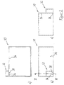
- Figures 1a, 1b and 1c show a first housing 10 in one Bottom, front and side view. The bottom view is shown in Figure 1a.
- a chamber 12 is on the left housing wall 14 integrally formed in the interior of the housing 10.
- a recess 16 in a wall 18 of the chamber 12 enables the laying of an electrical line (see FIG. 3) between the interior of the chamber 12 and the interior of the housing 10th
- Figure 1b Under the bottom view in Figure 1b is the front view of the Housing 10 shown. Another recess 20 in the Chamber 12 allows another line to be laid (see Figure 3) between the chamber 12 and the interior of the housing 10. A representation of section III-III is based on of Figure 3 explained in more detail.
- Figure 1c shows a side view of the housing 10. The expansion of the chamber 12 in its Longitudinal direction and its height, as well as its position in the housing 10 are clear in Figure 1c.
- FIGS 2a, b and c show a second housing 30 in one Bottom, front and side view.
- FIG 2a the bottom view of the housing 30 is shown.
- a chamber 32 is integrally formed on the wall 34 outside the housing 30.
- Two cutouts 36 and 38 in the housing wall 34 are used to hold electrical cables (see Figure 4) between chamber 32 and the interior of housing 30.
- FIG. 2b The front view is located below the bottom view in FIG. 2b the housing 30.
- a representation of the section IV-IV is explained below with reference to FIG. 4.
- Figure 2c shows the side view of the housing 30, the location of the Chamber 32 makes clear with respect to the housing 30.
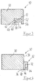
- FIG 3 shows the housing 10 as section III-III of Figure 1b.
- the interior of the housing 10 has a potting compound 50 filled out.
- the walls of the chamber 12 hold the sealing compound 50 from a PTC resistor 52.
- Leads 54 and 56 of the PTC resistors are connected via connection points 58 and 60 Lines 42 and 44 to one inside the potting compound 30 contained electronic unit connected.
- the administration 62 or 64 runs through the cutouts 16 or 20.
- Figure 4 shows the housing 30 as section IV-IV accordingly Figure 2b.
- the inside of the housing 30, which is also not one contains the transformer shown is with the sealing compound 70 filled.
- the housing wall 34 holds the sealing compound 50 from a PTC resistor 72 inside the chamber 32.
- a supply line 74 is via a junction 76 with a line 78 connected by the recess 36 from the chamber 32 extends inside the housing 30.
- Figures 5a, b and c show a first embodiment of a Closure one instead of the chamber 12 on the housing 10 molded chamber 12 'with a cap 90.
- the chamber 12 ' has reinforced walls. Between an inner wall 92 and an outer wall 94 of chamber 12 'is one Groove 96.
- Figure 5b shows the section V-V of the chamber 12 'of Figure 5a.
- the depth of the groove 96 can be seen in FIG. 5b. she agrees with the height of the cap 90 according to the figure 5c match.
- the closure cover 90 is designed that it is pressed into the groove 96 under pressure. Because of a snug fit creates a non-positive connection between Cap 90 and chamber 12 '. So that the chamber 12 'closed after inserting the PTC resistor 52 be so that the PTC resistance from environmental influences and is protected against unwanted touch.
- Figures 6a, b and c show a second embodiment a closure instead of the chamber 12 on the housing 10 molded chamber 12 "with a cap 100.
- Figure 6b shows the section VI-VI of the chamber 12 "according to Figure 6a.
- the depth of the holes 114 and 116 is too recognize that also corresponds to the depth of the bores 110 and 112.
- the opening of the chamber 12 " is chamfered.
- the in Figure 6c shown cap 100 is also in its Edge areas chamfered so that it optimally the chamber 12 " can close. There are locks in the corner areas of the cap 100 pins, of which in figure 6c pins 118 and 120 are shown.
- the length of the Pins 118 and 120 and their diameter match that Diameter and length of the associated bores 114 and 116 roughly match.
- the chamber 12 " is closed by inserting the cap 100 under pressure in the opening of the chamber 12 ". Due to a snug fit the Closure cover 100 held by the chamber 12 " is a secure closing and also an opening of the chamber 12 "possible at any time.
Landscapes
- Engineering & Computer Science (AREA)
- Power Engineering (AREA)
- Details Of Resistors (AREA)
- Casings For Electric Apparatus (AREA)
- Coils Or Transformers For Communication (AREA)
- Dc-Dc Converters (AREA)
- Housings And Mounting Of Transformers (AREA)
- Transformers For Measuring Instruments (AREA)
Description
- Figur 1a, b, c
- ein erstes Gehäuse in einer Unter-, Vorder- und Seitenansicht,
- Figur 2a, b, c
- ein zweites Gehäuse in einer Unter-, Vorder- und Seitenansicht,
- Figur 3
- den Schnitt III-III des Gehäuses nach Figur 1b,
- Figur 4
- den Schnitt IV-IV des Gehäuses nach Figur 2b,
- Figur 5a, b, c
- eine erste Ausführungsform eines Verschlusses einer Kammer des Gehäuses nach Figur 1a, 1b bzw. 1c, und
- Figur 6a, b, c
- eine zweite Ausführungsform eines Verschlusses einer Kammer des Gehäuses nach Figur 1a, 1b bzw. 1c.
Claims (14)
- Gehäuseanordnung zur vergossenen Aufnahme eines Transformators, der mit einem PTC-Widerstand (52, 72) verbunden ist, gekennzeichnet durch eine separate Kammer (12, 12', 12", 32) zur Aufnahme des PTC-Widerstands (52, 72).
- Gehäuseanordnung nach Anspruch 1, dadurch gekennzeichnet, daß die Kammer (12, 12', 12", 32) eine an einer Außenseite der Gehäuseanordnung liegende Öffnung hat.
- Gehäuseanordnung nach Anspruch 2, dadurch gekennzeichnet, daß die Öffnung mit einem Verschlußelement (90, 100) verschlossen ist.
- Gehäuseanordnung nach Anspruch 3, dadurch gekennzeichnet, daß das Verschlußelement durch einen Träger, auf dem die Gehäuseanordnung montiert ist, gebildet wird.
- Gehäuseanordnung nach Anspruch 3, dadurch gekennzeichnet, daß das Verschlußelement (90, 100) klappbar mit einer Seitenwand der Gehäuseanordnung verbunden ist.
- Gehäuseanordnung nach Anspruch 3, dadurch gekennzeichnet, daß das Verschlußelement (90, 100) durch Paßsitz mit der Öffnung verbunden ist.
- Gehäuseanordnung nach Anspruch 6, dadurch gekennzeichnet, daß der Paßsitz zwischen einer Nut (96) entlang der Öffnung und einem in die Nut (96) eingreifenden Vorsprung an einem der Öffnung angepaßten Deckel (90) vorhanden ist.
- Gehäuseanordnung nach Anspruch 6, dadurch gekennzeichnet, daß der Paßsitz zwischen Bohrungen (110 bis 116) an Formelementen (102 bis 108) in Ecken der Kammer (12") und in die Bohrung (110 bis 116) eingreifenden Stiften (118, 120) an einem die Öffnung verschließenden Deckel (100) vorhanden ist.
- Gehäuseanordnung nach einem der vorhergehenden Ansprüche, dadurch gekennzeichnet, daß die Kammer (12, 12', 12") in einem die Baueinheit aufnehmenden Gehäuse (10) angeordnet ist.
- Gehäuseanordnung nach einem der Ansprüche 1 bis 8, dadurch gekennzeichnet, daß die Kammer (32) außerhalb eines die Baueinheit aufnehmenden Gehäuses (30) angeordnet ist.
- Gehäuseanordnung nach einem der vorhergehenden Ansprüche, dadurch gekennzeichnet, daß die Kammer (12, 12', 12", 32) Aussparungen (16, 20 bzw. 36, 38) für den Transformator und den PTC-Widerstand (52, 72) verbindende Leitungen (62, 64 bzw. 78) hat.
- Gehäuseanordnung nach einem der Ansprüche 8 bis 10, dadurch gekennzeichnet, daß die Kammer (12, 12', 12", 32) am Gehäuse (10 bzw. 30) befestigt ist.
- Gehäuseanordnung nach Anspruch 11, dadurch gekennzeichnet, daß die Kammer (12, 12', 12", 32) einstückig am Gehäuse (10 bzw. 30) angeformt ist.
- Gehäuseanordnung nach Anspruch 11, dadurch gekennzeichnet, daß die Kammer mit einem Rastelement am Gehäuse (10, 30) befestigt ist.
Priority Applications (5)
| Application Number | Priority Date | Filing Date | Title |
|---|---|---|---|
| ES95118991T ES2149916T3 (es) | 1995-12-01 | 1995-12-01 | Caja destinada para contener un transformador. |
| PT95118991T PT777239E (pt) | 1995-12-01 | 1995-12-01 | Configuracao da caixa para incorperacao na moldagem por fundicao de um transformador |
| DE59508434T DE59508434D1 (de) | 1995-12-01 | 1995-12-01 | Gehäuseanordnung zur vergossenen Aufnahme eines Transformators |
| AT95118991T ATE193614T1 (de) | 1995-12-01 | 1995-12-01 | Gehäuseanordnung zur vergossenen aufnahme eines transformators |
| EP95118991A EP0777239B1 (de) | 1995-12-01 | 1995-12-01 | Gehäuseanordnung zur vergossenen Aufnahme eines Transformators |
Applications Claiming Priority (1)
| Application Number | Priority Date | Filing Date | Title |
|---|---|---|---|
| EP95118991A EP0777239B1 (de) | 1995-12-01 | 1995-12-01 | Gehäuseanordnung zur vergossenen Aufnahme eines Transformators |
Publications (2)
| Publication Number | Publication Date |
|---|---|
| EP0777239A1 EP0777239A1 (de) | 1997-06-04 |
| EP0777239B1 true EP0777239B1 (de) | 2000-05-31 |
Family
ID=8219861
Family Applications (1)
| Application Number | Title | Priority Date | Filing Date |
|---|---|---|---|
| EP95118991A Expired - Lifetime EP0777239B1 (de) | 1995-12-01 | 1995-12-01 | Gehäuseanordnung zur vergossenen Aufnahme eines Transformators |
Country Status (5)
| Country | Link |
|---|---|
| EP (1) | EP0777239B1 (de) |
| AT (1) | ATE193614T1 (de) |
| DE (1) | DE59508434D1 (de) |
| ES (1) | ES2149916T3 (de) |
| PT (1) | PT777239E (de) |
Families Citing this family (1)
| Publication number | Priority date | Publication date | Assignee | Title |
|---|---|---|---|---|
| FR2792110B1 (fr) * | 1999-04-06 | 2002-02-08 | Star Light | Transformateur pour lampe halogene |
Family Cites Families (6)
| Publication number | Priority date | Publication date | Assignee | Title |
|---|---|---|---|---|
| SE398280B (sv) * | 1975-11-20 | 1977-12-12 | Eldon Ab | Obegrensat kortslutningsseker elektrisk transformator |
| JPS56153720A (en) * | 1980-04-30 | 1981-11-27 | Hitachi Lighting Ltd | Molded stabilizer provided with protective device |
| JPS60213013A (ja) * | 1984-04-09 | 1985-10-25 | Matsushita Electric Ind Co Ltd | Acアダプタ− |
| US5204044A (en) * | 1989-03-28 | 1993-04-20 | Aisan Kogyo Kabushiki Kaisha | Method of asembling a DC solenoid with a thermistor |
| US5168422A (en) * | 1989-09-08 | 1992-12-01 | Allanson, Division Of Jannock Limited | Self-enclosed neon transformer |
| GB2236216B (en) * | 1989-09-12 | 1994-01-19 | Luminaire Dev Ltd | Transformer and connector assembly |
-
1995
- 1995-12-01 DE DE59508434T patent/DE59508434D1/de not_active Expired - Fee Related
- 1995-12-01 AT AT95118991T patent/ATE193614T1/de not_active IP Right Cessation
- 1995-12-01 ES ES95118991T patent/ES2149916T3/es not_active Expired - Lifetime
- 1995-12-01 PT PT95118991T patent/PT777239E/pt unknown
- 1995-12-01 EP EP95118991A patent/EP0777239B1/de not_active Expired - Lifetime
Also Published As
| Publication number | Publication date |
|---|---|
| ES2149916T3 (es) | 2000-11-16 |
| PT777239E (pt) | 2000-11-30 |
| EP0777239A1 (de) | 1997-06-04 |
| ATE193614T1 (de) | 2000-06-15 |
| DE59508434D1 (de) | 2000-07-06 |
Similar Documents
| Publication | Publication Date | Title |
|---|---|---|
| DE3807397A1 (de) | Heizgeraet | |
| DE102019203459A1 (de) | Vorrichtung und Verfahren zum Betreiben eines beheizbaren Sensors, insbesondere in einer explosionsfähigen Atmosphäre | |
| EP1116247A1 (de) | Ventilmagnet | |
| DE3924161C3 (de) | Elektrische Einrichtung | |
| DE19961360A1 (de) | Türaußengriffanordnung für eine Kraftfahrzeugtür | |
| DE4025993A1 (de) | Eingegossene sicherung ohne abschlusskappe | |
| DE10111336A1 (de) | Sensor, insbesondere Temperatur-Sensor, mit einem Messwiderstand | |
| EP0913882A2 (de) | Verfahren zum Isolieren eines elektrischen Bauteiles | |
| DE19712209A1 (de) | Hydraulikaggregat für hydraulische Steuer- und/oder Regelvorrichtung | |
| EP0777239A1 (de) | Gehäuseanordnung zur vergossenen Aufnahme einer elektronischen Baueinheit | |
| EP1043805B1 (de) | Elektrische Verbindungs- oder Anschlussklemme | |
| DE4038788A1 (de) | Gehaeuse fuer elektrische schaltungen | |
| DE29519091U1 (de) | Gehäuseanordnung zur vergossenen Aufnahme einer elektronischen Baueinheit | |
| EP0989567A1 (de) | Vergussgekapselte Vorrichtung | |
| EP1308978B1 (de) | Sicherungsgehäuse | |
| DE19513645C2 (de) | Klemmenanordnung | |
| DE102007051579A1 (de) | Stromwandler für die Messung und den Schutz in Hoch- oder Mittelspannungsnetzen | |
| DE9420607U1 (de) | Thermisches Sicherheitsventil | |
| DE202018001299U1 (de) | Verschließbares Bauelement wie Tür oder Fenster | |
| WO2005107029A1 (de) | Wassergekühlte steuereinrichtung für eine spritzgiessmaschine | |
| EP0340700B1 (de) | Gehäuse für Reihenschaltgerät | |
| DE7003178U (de) | Elektronisches geraet. | |
| CH689708A5 (de) | Gerätestecker mit Sicherung. | |
| DE19501895A1 (de) | Elektrische Schaltungsanordnung für Kraftfahrzeuge | |
| WO1997033290A2 (de) | Leistungsschalter mit isolierendem kontakthebelträger |
Legal Events
| Date | Code | Title | Description |
|---|---|---|---|
| PUAI | Public reference made under article 153(3) epc to a published international application that has entered the european phase |
Free format text: ORIGINAL CODE: 0009012 |
|
| AK | Designated contracting states |
Kind code of ref document: A1 Designated state(s): AT CH DE ES FR GB IT LI NL PT SE |
|
| AX | Request for extension of the european patent |
Free format text: LT;LV;SI |
|
| RBV | Designated contracting states (corrected) |
Designated state(s): AT CH DE ES FR GB IT LI NL PT SE |
|
| 17P | Request for examination filed |
Effective date: 19970701 |
|
| TPAD | Observations filed by third parties |
Free format text: ORIGINAL CODE: EPIDOS TIPA |
|
| TPAD | Observations filed by third parties |
Free format text: ORIGINAL CODE: EPIDOS TIPA |
|
| 17Q | First examination report despatched |
Effective date: 19990115 |
|
| RTI1 | Title (correction) |
Free format text: CASING ARRANGEMENT FOR CONTAINING A TRANSFORMATOR |
|
| GRAG | Despatch of communication of intention to grant |
Free format text: ORIGINAL CODE: EPIDOS AGRA |
|
| RTI1 | Title (correction) |
Free format text: CASING ARRANGEMENT FOR CONTAINING A TRANSFORMATOR |
|
| GRAG | Despatch of communication of intention to grant |
Free format text: ORIGINAL CODE: EPIDOS AGRA |
|
| GRAH | Despatch of communication of intention to grant a patent |
Free format text: ORIGINAL CODE: EPIDOS IGRA |
|
| GRAH | Despatch of communication of intention to grant a patent |
Free format text: ORIGINAL CODE: EPIDOS IGRA |
|
| GRAA | (expected) grant |
Free format text: ORIGINAL CODE: 0009210 |
|
| RTI1 | Title (correction) |
Free format text: CASING ARRANGEMENT FOR CONTAINING A TRANSFORMER |
|
| AK | Designated contracting states |
Kind code of ref document: B1 Designated state(s): AT CH DE ES FR GB IT LI NL PT SE |
|
| REF | Corresponds to: |
Ref document number: 193614 Country of ref document: AT Date of ref document: 20000615 Kind code of ref document: T |
|
| REG | Reference to a national code |
Ref country code: CH Ref legal event code: EP |
|
| REG | Reference to a national code |
Ref country code: CH Ref legal event code: NV Representative=s name: PATENTANWALTSBUERO FELDMANN AG |
|
| REF | Corresponds to: |
Ref document number: 59508434 Country of ref document: DE Date of ref document: 20000706 |
|
| ITF | It: translation for a ep patent filed | ||
| ET | Fr: translation filed | ||
| GBT | Gb: translation of ep patent filed (gb section 77(6)(a)/1977) |
Effective date: 20000821 |
|
| REG | Reference to a national code |
Ref country code: ES Ref legal event code: FG2A Ref document number: 2149916 Country of ref document: ES Kind code of ref document: T3 |
|
| REG | Reference to a national code |
Ref country code: PT Ref legal event code: SC4A Free format text: AVAILABILITY OF NATIONAL TRANSLATION Effective date: 20000830 |
|
| PLBE | No opposition filed within time limit |
Free format text: ORIGINAL CODE: 0009261 |
|
| STAA | Information on the status of an ep patent application or granted ep patent |
Free format text: STATUS: NO OPPOSITION FILED WITHIN TIME LIMIT |
|
| 26N | No opposition filed | ||
| REG | Reference to a national code |
Ref country code: GB Ref legal event code: IF02 |
|
| PGFP | Annual fee paid to national office [announced via postgrant information from national office to epo] |
Ref country code: PT Payment date: 20021204 Year of fee payment: 8 |
|
| PGFP | Annual fee paid to national office [announced via postgrant information from national office to epo] |
Ref country code: GB Payment date: 20021219 Year of fee payment: 8 |
|
| PGFP | Annual fee paid to national office [announced via postgrant information from national office to epo] |
Ref country code: AT Payment date: 20030110 Year of fee payment: 8 |
|
| PGFP | Annual fee paid to national office [announced via postgrant information from national office to epo] |
Ref country code: NL Payment date: 20030120 Year of fee payment: 8 Ref country code: FR Payment date: 20030120 Year of fee payment: 8 |
|
| PGFP | Annual fee paid to national office [announced via postgrant information from national office to epo] |
Ref country code: SE Payment date: 20030127 Year of fee payment: 8 Ref country code: CH Payment date: 20030127 Year of fee payment: 8 |
|
| PGFP | Annual fee paid to national office [announced via postgrant information from national office to epo] |
Ref country code: ES Payment date: 20030130 Year of fee payment: 8 Ref country code: DE Payment date: 20030130 Year of fee payment: 8 |
|
| PG25 | Lapsed in a contracting state [announced via postgrant information from national office to epo] |
Ref country code: GB Free format text: LAPSE BECAUSE OF NON-PAYMENT OF DUE FEES Effective date: 20031201 Ref country code: AT Free format text: LAPSE BECAUSE OF NON-PAYMENT OF DUE FEES Effective date: 20031201 |
|
| PG25 | Lapsed in a contracting state [announced via postgrant information from national office to epo] |
Ref country code: SE Free format text: LAPSE BECAUSE OF NON-PAYMENT OF DUE FEES Effective date: 20031202 Ref country code: ES Free format text: LAPSE BECAUSE OF NON-PAYMENT OF DUE FEES Effective date: 20031202 |
|
| PG25 | Lapsed in a contracting state [announced via postgrant information from national office to epo] |
Ref country code: LI Free format text: LAPSE BECAUSE OF NON-PAYMENT OF DUE FEES Effective date: 20031231 Ref country code: CH Free format text: LAPSE BECAUSE OF NON-PAYMENT OF DUE FEES Effective date: 20031231 |
|
| PG25 | Lapsed in a contracting state [announced via postgrant information from national office to epo] |
Ref country code: PT Free format text: LAPSE BECAUSE OF NON-PAYMENT OF DUE FEES Effective date: 20040630 |
|
| PG25 | Lapsed in a contracting state [announced via postgrant information from national office to epo] |
Ref country code: NL Free format text: LAPSE BECAUSE OF NON-PAYMENT OF DUE FEES Effective date: 20040701 Ref country code: DE Free format text: LAPSE BECAUSE OF NON-PAYMENT OF DUE FEES Effective date: 20040701 |
|
| GBPC | Gb: european patent ceased through non-payment of renewal fee |
Effective date: 20031201 |
|
| EUG | Se: european patent has lapsed | ||
| REG | Reference to a national code |
Ref country code: CH Ref legal event code: PL |
|
| PG25 | Lapsed in a contracting state [announced via postgrant information from national office to epo] |
Ref country code: FR Free format text: LAPSE BECAUSE OF NON-PAYMENT OF DUE FEES Effective date: 20040831 |
|
| NLV4 | Nl: lapsed or anulled due to non-payment of the annual fee |
Effective date: 20040701 |
|
| REG | Reference to a national code |
Ref country code: FR Ref legal event code: ST |
|
| REG | Reference to a national code |
Ref country code: PT Ref legal event code: MM4A Free format text: LAPSE DUE TO NON-PAYMENT OF FEES Effective date: 20040630 |
|
| REG | Reference to a national code |
Ref country code: ES Ref legal event code: FD2A Effective date: 20031202 |
|
| PG25 | Lapsed in a contracting state [announced via postgrant information from national office to epo] |
Ref country code: IT Free format text: LAPSE BECAUSE OF NON-PAYMENT OF DUE FEES;WARNING: LAPSES OF ITALIAN PATENTS WITH EFFECTIVE DATE BEFORE 2007 MAY HAVE OCCURRED AT ANY TIME BEFORE 2007. THE CORRECT EFFECTIVE DATE MAY BE DIFFERENT FROM THE ONE RECORDED. Effective date: 20051201 |