EP0779556A2 - Verfahren zur Herstellung einer Halbleiteranordnung - Google Patents
Verfahren zur Herstellung einer Halbleiteranordnung Download PDFInfo
- Publication number
- EP0779556A2 EP0779556A2 EP96119868A EP96119868A EP0779556A2 EP 0779556 A2 EP0779556 A2 EP 0779556A2 EP 96119868 A EP96119868 A EP 96119868A EP 96119868 A EP96119868 A EP 96119868A EP 0779556 A2 EP0779556 A2 EP 0779556A2
- Authority
- EP
- European Patent Office
- Prior art keywords
- film
- resist pattern
- region
- insulating film
- conductive film
- Prior art date
- Legal status (The legal status is an assumption and is not a legal conclusion. Google has not performed a legal analysis and makes no representation as to the accuracy of the status listed.)
- Granted
Links
Images




Classifications
-
- H—ELECTRICITY
- H10—SEMICONDUCTOR DEVICES; ELECTRIC SOLID-STATE DEVICES NOT OTHERWISE PROVIDED FOR
- H10P—GENERIC PROCESSES OR APPARATUS FOR THE MANUFACTURE OR TREATMENT OF DEVICES COVERED BY CLASS H10
- H10P76/00—Manufacture or treatment of masks on semiconductor bodies, e.g. by lithography or photolithography
-
- H—ELECTRICITY
- H10—SEMICONDUCTOR DEVICES; ELECTRIC SOLID-STATE DEVICES NOT OTHERWISE PROVIDED FOR
- H10P—GENERIC PROCESSES OR APPARATUS FOR THE MANUFACTURE OR TREATMENT OF DEVICES COVERED BY CLASS H10
- H10P50/00—Etching of wafers, substrates or parts of devices
- H10P50/71—Etching of wafers, substrates or parts of devices using masks for conductive or resistive materials
-
- G—PHYSICS
- G03—PHOTOGRAPHY; CINEMATOGRAPHY; ANALOGOUS TECHNIQUES USING WAVES OTHER THAN OPTICAL WAVES; ELECTROGRAPHY; HOLOGRAPHY
- G03F—PHOTOMECHANICAL PRODUCTION OF TEXTURED OR PATTERNED SURFACES, e.g. FOR PRINTING, FOR PROCESSING OF SEMICONDUCTOR DEVICES; MATERIALS THEREFOR; ORIGINALS THEREFOR; APPARATUS SPECIALLY ADAPTED THEREFOR
- G03F7/00—Photomechanical, e.g. photolithographic, production of textured or patterned surfaces, e.g. printing surfaces; Materials therefor, e.g. comprising photoresists; Apparatus specially adapted therefor
- G03F7/0035—Multiple processes, e.g. applying a further resist layer on an already in a previously step, processed pattern or textured surface
-
- H—ELECTRICITY
- H10—SEMICONDUCTOR DEVICES; ELECTRIC SOLID-STATE DEVICES NOT OTHERWISE PROVIDED FOR
- H10D—INORGANIC ELECTRIC SEMICONDUCTOR DEVICES
- H10D64/00—Electrodes of devices having potential barriers
- H10D64/01—Manufacture or treatment
- H10D64/013—Manufacture or treatment of electrodes having a conductor capacitively coupled to a semiconductor by an insulator
- H10D64/01302—Manufacture or treatment of electrodes having a conductor capacitively coupled to a semiconductor by an insulator the insulator being formed after the semiconductor body, the semiconductor being silicon
- H10D64/01304—Manufacture or treatment of electrodes having a conductor capacitively coupled to a semiconductor by an insulator the insulator being formed after the semiconductor body, the semiconductor being silicon characterised by the conductor
- H10D64/01326—Aspects related to lithography, isolation or planarisation of the conductor
-
- Y—GENERAL TAGGING OF NEW TECHNOLOGICAL DEVELOPMENTS; GENERAL TAGGING OF CROSS-SECTIONAL TECHNOLOGIES SPANNING OVER SEVERAL SECTIONS OF THE IPC; TECHNICAL SUBJECTS COVERED BY FORMER USPC CROSS-REFERENCE ART COLLECTIONS [XRACs] AND DIGESTS
- Y10—TECHNICAL SUBJECTS COVERED BY FORMER USPC
- Y10S—TECHNICAL SUBJECTS COVERED BY FORMER USPC CROSS-REFERENCE ART COLLECTIONS [XRACs] AND DIGESTS
- Y10S430/00—Radiation imagery chemistry: process, composition, or product thereof
- Y10S430/143—Electron beam
Definitions
- the present invention relates to a method of fabricating a semiconductor device and more particularly to a method of fabricating a semiconductor device by forming resist masks by using both photo-lithography and electron beam lithography and by using them as patterning masks of underlying layers.
- steps of forming a conductive film on the whole surface of a semiconductor substrate and of patterning and processing it into a predetermined shape to form a wiring layer and the like are implemented in fabricating semiconductor devices.
- steps of forming a gate electrode wire and a wire connecting region of a MOS transistor will be explained below as conventional technology with reference to FIGs. 1 through 3. It is noted that in the following explanation, the wire connecting region is assumed to be connected with the gate electrode wire. Further, it is assumed that this wire connecting region is formed to be properly positioned and so that its size is larger than the gate electrode wire in order to contact a wiring layer which is not shown in the figures.
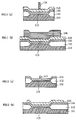
- FIGs. 1(a), 2(a) and 3(a) is a sectional view of a part corresponding to a section along a line A-A in FIG. 4(c) and each of FIGs. 1(b), 2(b) and 3(b) is a sectional view of a part corresponding to a section along a line B-B in FIG. 4(c).
- a field insulating film 112 is formed on an element separating region of a semiconductor substrate 111 and a gate insulating film 113 is formed on an element region of the semiconductor substrate 111 as shown in FIGs. 1(a) and 1(b). While a case in which the field insulating film 112 is formed by means of LOCOS (Local Oxidation of Silicon) is shown in the figures, it may also be formed by means of STI (Shallow Trench Isolation).
- a conductive film 114 is formed on these insulating films 112 and 113 as a polycrystal silicon film or the like to form the gate electrode wire. Then, a cap insulating film 115 is formed on the conductive film 114.
- the conductive film 114 and the cap insulating film 115 are deposited by means of CVD (Chemical Vapour Deposition) or sputtering. After that, a resist for photo-lithography or for electron beam lithography is applied on the cap insulating film 115 and a resist pattern 116 is formed by exposing the resist into the shape of the gate electrode wire by means of photo-lithography or electron beam lithography and by developing the exposed resist.
- CVD Chemical Vapour Deposition
- the cap insulating film 115 is patterned by means of anisotropic etching by using the resist pattern 116 as a mask as shown in FIGs. 2(a) and 2(b).
- the resist pattern 116 used as the mask in etching is removed by means of ashing or the like.
- the conductive film 114 is patterned by means of anisotropic etching by using the patterned cap insulating film 115 as a mask to form the gate electrode wire and the wiring connecting section connected thereto as shown in FIGs. 3(a) and 3(b).
- Photo-lithography is a method normally used in forming a resist pattern and is suited for mass-production of semiconductor devices because its throughput is relatively high. However, it has a problem in terms of resolution in view of the fabrication of ultra LSIs which will be refined further in the future. According to the present photo-lithography technology, a width of about 0.25 ⁇ m is considered to be the limit in patterning even if a KrF excimer laser is used as a light source. While the design rule for wiring is predicted to become around 0.1 ⁇ m or less following the trend of the refinement of ultra LSIs of the future, it is difficult to pattern a wire to meet such a design rule by using the present photo-lithography technology.
- electron beam lithography has a higher resolution as compared to photo-lithography and is considered to be fully able to enable patterning to meet the design rule of around 0.1 ⁇ m or less.
- it has had a problem that its throughput is extremely low. This is because, while a plane of a resist can be exposed in a wide range at one time by photo-lithography, the plane of the resist cannot be exposed in a wide range at one time by electron beam lithography and it is necessary to, trace a pattern on a region to be exposed with the electron beam.
- a pattern whose design rule is relatively large i.e., a pattern which can be fully patterned even by using the present photo-lithography techniques
- a pattern whose design rule is relatively small i.e., a pattern which is difficult to pattern by the present photo-lithography techniques
- an area of the pattern whose design rule is relatively large is larger than an area of a pattern whose rule is relatively small. It is then conceivable to use electron beam lithography only in forming the pattern whose design rule is small and which is hard to pattern by photo-lithography and to use photo-lithography in forming patterns other than that in order to improve both the throughput and the resolution.
- a method of fabricating a semiconductor device comprising steps of forming a first insulating film, a conductive film, a second insulating film and a selected film whose etching characteristic is substantially the same as that of the conductive film sequentially on a semiconductor substrate having first and second regions; forming a first resist pattern in the first region on the selected film by means of photo-lithography; patterning the selected film by using the first resist pattern as a mask; removing the first resist pattern; forming a second resist pattern in the second region on the surface of at least the second insulating film by means of electron beam lithography; patterning the second insulating film by using the second resist pattern and the selected film as masks; removing the second resist pattern; and patterning the conductive film by using the patterned second insulating film as a mask.
- a method of fabricating a semiconductor device comprising steps of forming a first insulating film, a conductive film, a second insulating film and a selected film whose etching characteristic is substantially the same as that of the conductive film sequentially on a semiconductor substrate having first and second regions; forming a second resist pattern in the second region on the selected film by means of electron beam lithography; patterning the selected film by using the second resist pattern as a mask; removing the second resist pattern; forming a first resist pattern in the first region on at least the second insulating film by means of photo-lithography; patterning the second insulating film by using the first resist pattern and the selected film as masks; removing the first resist pattern; and patterning the conductive film by using the patterned second insulating film as a mask.
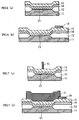
- FIG. 4(c) is a schematic top view of the MOS transistor after forming each element.
- Fig. 4(c) shows a region 211 in which the gate electrode wire is formed, an element region 212 in which an element is formed, an element separating region 213 and a region 214 in which the wire connecting region is formed.
- FIGs. 4(a) through 9(a) shows a sectional view which corresponds to a section along a line A-A in FIG.
- FIGs. 4(b) through 9(b) shows a sectional view which corresponds to a section along a line B-B in FIG. 4(c), i.e., a section in the direction parallel to the gate electrode wire. It is assumed that the wire connecting region is formed to have a larger dimension as compared to the gate electrode wire and is positioned to contact an upper wiring layer which is not shown.
- a field insulating film 12 is formed in the element separating region 213 on a semiconductor substrate 11 as shown in FIGs. 4(a) and 4(b) by means of LOCOS. It may also be formed by means of STI, instead of LOCOS.
- gate oxidation is implemented to form a gate insulating film 13 having a thickness of 5 to 20 nm on the element region 212.
- a conductive film 14 of 100 to 400 nm in thickness is formed by means of CVD or sputtering on the gate insulating film 13 to form the gate electrode wire.
- a cap insulating film 15 of about 200 nm in thickness is then formed on the conductive film 14 by means of CVD or the like.
- a film 16 whose etching characteristic is substantially the same as that of the conductive film 14 and which has a thickness equal to or less than that of the conductive film 14 is formed on the cap insulating film 15.
- the conductive film 14 is formed of polycrystal silicon containing a high concentration of phosphorus or boron or a high-melting point metal such as tungsten, or of a layered structure in which a high-melting point metal silicide such as tungsten silicide or molybdenum silicide is used for the upper layer and polycrystal silicon is used for the lower layer, or of a layered structure in which a high-melting point metal such as tungsten or molybdenum is used for the upper layer and polycrystal silicon is used for the lower layer.
- the cap insulating film 15 is formed of a material which allows enough selectivity in etching relative to the conductive film 14,e.g., of a silicon oxide film, a silicon nitrate film or the like.
- the film 16 is formed of a material having an etching characteristic which is substantially the same as that of the conductive film 14, so that it is removed by etching during a step of patterning the conductive layer 14.
- film 16 can, for example, be formed of the same material that used for forming the whole or part of the conductive film 14, a material containing the material of the conductive film 14, e.g., polycrystal silicon, high-melting point metal or high-melting point metal silicide, or a material containing more than one of them. It is desirable to form the film 16 of polycrystal silicon because the selectivity in etching of the high-melting point metal or high-melting point metal silicide is around several times relative to polycrystal silicon.
- the film 16 of polycrystal silicon when the conductive film 14 is formed of a single layer of polycrystal silicon or high-melting point metal or when the conductive film 14 is formed by layering high-melting point metal or high-melting point metal silicide and polycrystal silicon.
- the film 16 is formed of polycrystal silicon
- a resist for photo-lithography is applied on the whole surface of the film 16 as shown in FIGs. 5(a) and 5(b). Then, the resist is exposed in a predetermined pattern by means of photo-lithography and is developed to form a resist pattern 21.
- This resist pattern 21 is formed on a region where the design rule is relatively large and which can be fully achieved by photo-lithography. That is, it is not formed on a region such as the gate electrode wire which is difficult to form by photo-lithography but, instead, on a region such as the wire connecting region and a pad for connecting with upper layer wires. While it is presently possible to pattern a line width of about 0.25 ⁇ m by photo-lithography, the resist pattern is formed here to have a dimension of length and breadth of about 0.8 to 1.4 ⁇ m.
- the film 16 is etched by means of anisotropic etching by using the resist pattern 21 as a mask as shown in FIGs 6(a) and 6(b).
- the selectivity in etching of the cap insulating film 15 relative to the film 16 is high, it is possible to etch only the film 16 and to leave unaffected the cap insulating film 15.
- the selectivity in etching the insulating film may be increased to about 10 to 30 times that of the film 16 by using Cl2, HBr, SF6 or the like as the etching gas in etching the film 16.
- the resist pattern 21 is removed by means of ashing or by a combination of ashing and chemical treatment with sulfuric acid and hydrogen peroxide.
- a resist for electron beam lithography is applied on the cap insulating film 15 and the patterned film 16.
- a resist pattern 41 is formed by exposing the resist by means of electron beam lithography and developing only the part which corresponds to the gate electrode wire and which is difficult to pattern by photo-lithography. While it is possible to pattern a line width of about 0.1 ⁇ m or less by electron beam lithography, the resist pattern is formed here to have a line width of about 0.15 ⁇ m.
- the cap insulating film 15 is etched by means of anisotropic etching by using both the resist pattern 41 and the film 16, whose patterning has been completed by the previous processing steps, as masks as shown in FIGs. 8(a) and 8(b).
- the selectivity in etching of the cap insulating film 15 relative to the conductive film 14 and to the film 16 is relatively high, it is possible to etch only the cap insulating film 15 and to leave the conductive film 14 and the film 16.
- the selectivity in etching relative to the conductive film may be increased to about 10 to 30 times that of the film 16 by combining and using CF 4 , CO, CHF 3 and the like as etching gas in etching the cap insulating film 15.
- the resist pattern 41 is removed by means of ashing or by a combination of ashing and chemical treatment with sulfuric acid and hydrogen peroxide.
- the conductive film 14 is etched by means of anisotropic etching by using the cap insulating film 15 as a mask as shown in FIGs. 9(a) and 9(b).
- the film 16 is formed of the material whose etching characteristic is substantially the same as that of the conductive film 14, it is etched and removed at the same time with the etching of the conductive film 14. Accordingly, a step for removing the film 16 may be omitted.
- the selectivity in etching the cap insulating film 15 may be increased to about 10 to 30 times by using Cl2, HBr, SF6 or the like as etching gas in etching the conductive film 14.
- the film 16 whose etching characteristic is substantially the same as that of the conductive film 14 is formed on the cap insulating film 15. Then, after forming the resist pattern 21 for the region whose design rule is large and which can be handled by the photo-lithography technology, the film 16 is patterned by using the resist pattern 21 as a mask. Next, the resist pattern 41 which is the part which is difficult to handle by the photo-lithography technology is formed by using electron beam lithography and the cap insulating film 15 is patterned by using the resist pattern 41 and the patterned film 16 as masks. Then, finally, the conductive film 14 is patterned by using the patterned cap insulating film 15 as a mask. At the same time, the film 16 is removed with the conductive film 14, so that a step for removing the film 16 may be omitted.
- FIGs. 10(a) through 14(b) are sectional views which corresponds to the section along the line A-A in FIG. 4(c) and each of FIGs. 10(b) through 14(b) is a sectional view which corresponds to the section along the line B-B in FIG. 4(c).
- the field insulating film 12, the gate insulating film 13, the conductive film 14, the cap insulating film 15 and the film 16 are formed sequentially on the semiconductor substrate 11 as shown in FIGs. 10(a) and 10(b). These steps are the same as those shown in FIGs. 4(a) through 4(c) in the first embodiment. Then, a resist for electron beam lithography is applied on the film 16 and only the region which is difficult to handle by photo-lithography is patterned by means of electron beam lithography to form a resist pattern 71.
- the film 16 is etched by means of anisotropic etching by using the resist pattern 71 as a mask as shown in FIGs. 11(a) and 11(b).
- the resist pattern 71 is removed by means of ashing or by a combination of ashing and chemical treatment with sulfuric acid and hydrogen peroxide.
- a resist for photo-lithography is applied on the cap insulating film 15 and the film 16.
- a resist pattern 91 is formed by exposing and developing the resist into a predetermined pattern by using photo-lithography.
- This resist pattern 91 is formed on a region where the design rule is relatively large and which can be fully handled by photo-lithography. That is, it is formed not on a region like the gate electrode wire which is difficult to handle by photo-lithography, but on a region which corresponds to the part for forming the wire connecting region or the pad for connecting with upper layer wires.
- the cap insulating film 15 is etched by means of anisotropic etching by using both the resist pattern 91 and the film 16 as masks as shown in FIGs. 13(a) and 13(b). At this time, because the selectivity in etching of the cap insulating film 15 relative to the conductive film 14 and to the film 16 is high, it is possible to pattern only the cap insulating film 15 and to leave the conductive film 14 and the film 16.
- the resist pattern 91 is removed by means of ashing or by combination of ashing and chemical treatment with sulfuric acid and hydrogen peroxide.
- the conductive film 14 is etched by means of anisotropic etching by using the cap insulating film 15 as a mask as shown in FIGs. 14(a) and 14(b).
- the film 16 is formed of the material whose etching characteristic is substantially the same as that of the conductive film 14, it is etched and removed at the same time with the conductive film 14. Accordingly, a separate step of removing the film 16 may be omitted. Thus, the steps for forming the gate electrode wire and the wire connecting region connected thereto are completed.
- the film 16 whose etching characteristic is substantially the same as that of the conductive film 14 is formed on the cap insulating film 15 similarly to the first embodiment.
- the resist pattern 71 is formed by using electron beam lithography in a region which is difficult to handle by photo-lithography technology at first and the film 16 is patterned by using it as a mask.
- the cap insulating film 15 is patterned by using the film 16 and the pattern 91 as masks.
- the conductive film 14 is patterned by using the patterned cap insulating film 15 as a mask.
- the film 16 is removed with the conductive film 14, so that a step for removing the film 16 may be omitted.
- the sequence of forming the resist pattern by using photo-lithography and of forming the resist pattern by using electron beam lithography are different in the first and second embodiments.
- the thickness of the film 16 may be equal to or greater than that of the conductive film 14 in the embodiments described above so long as it has such a characteristic that it is removed at the same time in the step of etching the conductive film.
- the steps for forming the gate electrode wire and the wire connecting region have been exemplified in the embodiments described above, the present invention is not confined only to them and may be applied to steps for forming wiring layers in general in which a conductive film and an insulating film are layered. Also, it may be applied to steps for forming a resistor element formed by a conductive film having a high resistance on a semiconductor substrate and for forming a connecting terminal connected to the resistor element. That is, because electron beam lithography allows a region whose line width is narrow to be patterned, a resistor element having a higher resistance may be formed in a very small region.
Landscapes
- Physics & Mathematics (AREA)
- General Physics & Mathematics (AREA)
- Internal Circuitry In Semiconductor Integrated Circuit Devices (AREA)
- Electron Beam Exposure (AREA)
Applications Claiming Priority (3)
| Application Number | Priority Date | Filing Date | Title |
|---|---|---|---|
| JP321535/95 | 1995-12-11 | ||
| JP32153595 | 1995-12-11 | ||
| JP32153595 | 1995-12-11 |
Publications (3)
| Publication Number | Publication Date |
|---|---|
| EP0779556A2 true EP0779556A2 (de) | 1997-06-18 |
| EP0779556A3 EP0779556A3 (de) | 1997-07-02 |
| EP0779556B1 EP0779556B1 (de) | 2001-10-04 |
Family
ID=18133654
Family Applications (1)
| Application Number | Title | Priority Date | Filing Date |
|---|---|---|---|
| EP96119868A Expired - Lifetime EP0779556B1 (de) | 1995-12-11 | 1996-12-11 | Verfahren zur Herstellung einer Halbleiteranordnung |
Country Status (4)
| Country | Link |
|---|---|
| US (1) | US5916733A (de) |
| EP (1) | EP0779556B1 (de) |
| KR (1) | KR100225831B1 (de) |
| DE (1) | DE69615642T2 (de) |
Cited By (2)
| Publication number | Priority date | Publication date | Assignee | Title |
|---|---|---|---|---|
| WO2001096957A1 (fr) * | 2000-06-16 | 2001-12-20 | Commissariat A L'energie Atomique | Procede de creation d'un etage de circuit integre ou coexistent des motifs fins et larges |
| WO2007116362A1 (en) * | 2006-04-07 | 2007-10-18 | Nxp B.V. | Method of manufacturing a semiconductor device |
Families Citing this family (9)
| Publication number | Priority date | Publication date | Assignee | Title |
|---|---|---|---|---|
| US6312874B1 (en) * | 1998-11-06 | 2001-11-06 | Advanced Micro Devices, Inc. | Method for forming a dual damascene trench and underlying borderless via in low dielectric constant materials |
| US6218056B1 (en) * | 1999-03-30 | 2001-04-17 | International Business Machines Corporation | Method of making highly defined bilayer lift-off mask |
| US7071121B2 (en) * | 2003-10-28 | 2006-07-04 | Hewlett-Packard Development Company, L.P. | Patterned ceramic films and method for producing the same |
| DE102004056369B4 (de) * | 2004-11-22 | 2008-08-28 | Renk Ag | Betätigungseinrichtung für Fahrzeuggetriebe von Kettenfahrzeugen oder Radfahrzeugen mit Radseitenlenkung |
| US8048764B2 (en) * | 2009-09-30 | 2011-11-01 | Taiwan Semiconductor Manufacturing Co., Ltd. | Dual etch method of defining active area in semiconductor device |
| CN103390584A (zh) * | 2012-05-09 | 2013-11-13 | 中国科学院微电子研究所 | 半导体器件的制造方法 |
| US8906244B2 (en) * | 2012-10-25 | 2014-12-09 | The United States Of America As Represented By The Secretary Of The Army | Method for forming a device having nanopillar and cap structures |
| US10083781B2 (en) | 2015-10-30 | 2018-09-25 | Vishay Dale Electronics, Llc | Surface mount resistors and methods of manufacturing same |
| US10438729B2 (en) | 2017-11-10 | 2019-10-08 | Vishay Dale Electronics, Llc | Resistor with upper surface heat dissipation |
Family Cites Families (10)
| Publication number | Priority date | Publication date | Assignee | Title |
|---|---|---|---|---|
| JPS5669835A (en) * | 1979-11-09 | 1981-06-11 | Japan Electronic Ind Dev Assoc<Jeida> | Method for forming thin film pattern |
| EP0037708B1 (de) * | 1980-04-02 | 1986-07-30 | Hitachi, Ltd. | Verfahren zur Herstellung eines Musters |
| JPS5968928A (ja) * | 1982-10-13 | 1984-04-19 | Pioneer Electronic Corp | 半導体装置の製造方法 |
| US4591547A (en) * | 1982-10-20 | 1986-05-27 | General Instrument Corporation | Dual layer positive photoresist process and devices |
| US4610948A (en) * | 1984-01-25 | 1986-09-09 | The United States Of America As Represented By The Secretary Of The Army | Electron beam peripheral patterning of integrated circuits |
| US4612274A (en) * | 1985-11-18 | 1986-09-16 | Motorola, Inc. | Electron beam/optical hybrid lithographic resist process in acoustic wave devices |
| US5194749A (en) * | 1987-11-30 | 1993-03-16 | Hitachi, Ltd. | Semiconductor integrated circuit device |
| US5034091A (en) * | 1990-04-27 | 1991-07-23 | Hughes Aircraft Company | Method of forming an electrical via structure |
| KR100188508B1 (ko) * | 1993-03-26 | 1999-06-01 | 세끼사와 다까시 | 비정질탄소막을 사용하는 패턴형성방법과 에칭방법 및 비정질탄소막 형성방법 |
| JP2803999B2 (ja) * | 1993-11-10 | 1998-09-24 | 現代電子産業株式会社 | 半導体装置の微細パターン製造法 |
-
1996
- 1996-12-10 US US08/762,856 patent/US5916733A/en not_active Expired - Fee Related
- 1996-12-11 KR KR1019960064114A patent/KR100225831B1/ko not_active Expired - Fee Related
- 1996-12-11 EP EP96119868A patent/EP0779556B1/de not_active Expired - Lifetime
- 1996-12-11 DE DE69615642T patent/DE69615642T2/de not_active Expired - Lifetime
Cited By (4)
| Publication number | Priority date | Publication date | Assignee | Title |
|---|---|---|---|---|
| WO2001096957A1 (fr) * | 2000-06-16 | 2001-12-20 | Commissariat A L'energie Atomique | Procede de creation d'un etage de circuit integre ou coexistent des motifs fins et larges |
| FR2810447A1 (fr) * | 2000-06-16 | 2001-12-21 | Commissariat Energie Atomique | Procede de creation d'un etage de circuit integre ou conexistent des motifs fins et larges |
| US6727179B2 (en) | 2000-06-16 | 2004-04-27 | Commissariat A L'energie Atomique | Method for creating an integrated circuit stage wherein fine and large patterns coexist |
| WO2007116362A1 (en) * | 2006-04-07 | 2007-10-18 | Nxp B.V. | Method of manufacturing a semiconductor device |
Also Published As
| Publication number | Publication date |
|---|---|
| DE69615642D1 (de) | 2001-11-08 |
| KR970051945A (ko) | 1997-07-29 |
| EP0779556A3 (de) | 1997-07-02 |
| EP0779556B1 (de) | 2001-10-04 |
| US5916733A (en) | 1999-06-29 |
| DE69615642T2 (de) | 2002-08-01 |
| KR100225831B1 (ko) | 1999-10-15 |
Similar Documents
| Publication | Publication Date | Title |
|---|---|---|
| KR920004654B1 (ko) | 주문된 집적회로의 제조방법 | |
| US20080251951A1 (en) | Use of a dual tone resist to form photomasks and intermediate semiconductor device structures | |
| US20080203590A1 (en) | Integrated circuit semiconductor device with overlay key and alignment key and method of fabricating the same | |
| US6111319A (en) | Method of forming submicron contacts and vias in an integrated circuit | |
| US5916733A (en) | Method of fabricating a semiconductor device | |
| GB2100926A (en) | Field effect transistors | |
| US10410863B2 (en) | Methods for integrated circuit design and fabrication | |
| KR100225327B1 (ko) | 폴리사이드 구조를 갖는 반도체장치 및 그의 제조방법 | |
| KR100443064B1 (ko) | 집적 회로내의 소규모 구조 형성을 위한 이미지 리버설 방법 | |
| US5776836A (en) | Self aligned method to define features smaller than the resolution limit of a photolithography system | |
| US6448179B2 (en) | Method for fabricating semiconductor device | |
| US5902133A (en) | Method of forming a narrow polysilicon gate with i-line lithography | |
| US7910289B2 (en) | Use of dual mask processing of different composition such as inorganic/organic to enable a single poly etch using a two-print-two-etch approach | |
| US5902717A (en) | Method of fabricating semiconductor device using half-tone phase shift mask | |
| JP3607022B2 (ja) | 半導体装置の製造方法 | |
| JPH11204506A (ja) | 回路パターンが形成されたウェハおよびその製造方法 | |
| US5338397A (en) | Method of forming a semiconductor device | |
| KR100284071B1 (ko) | 반도체소자의 콘택 제조방법 | |
| JPH0327521A (ja) | Mos型トランジスタの製造方法 | |
| US20020177085A1 (en) | Self-aligned photolithographic process for forming silicon-on-insulator devices | |
| JPH04291345A (ja) | パターン形成方法 | |
| KR0158903B1 (ko) | 반도체소자의 게이트전극 콘택 및 그 제조방법 | |
| KR0166488B1 (ko) | 반도체 소자의 미세콘택 형성방법 | |
| US20030215752A1 (en) | Device manufacturing method | |
| KR20000043205A (ko) | 반도체소자의 콘택홀 형성방법 |
Legal Events
| Date | Code | Title | Description |
|---|---|---|---|
| PUAI | Public reference made under article 153(3) epc to a published international application that has entered the european phase |
Free format text: ORIGINAL CODE: 0009012 |
|
| PUAL | Search report despatched |
Free format text: ORIGINAL CODE: 0009013 |
|
| 17P | Request for examination filed |
Effective date: 19961211 |
|
| AK | Designated contracting states |
Kind code of ref document: A2 Designated state(s): DE FR GB |
|
| AK | Designated contracting states |
Kind code of ref document: A3 Designated state(s): DE FR GB |
|
| 17Q | First examination report despatched |
Effective date: 19990525 |
|
| GRAG | Despatch of communication of intention to grant |
Free format text: ORIGINAL CODE: EPIDOS AGRA |
|
| GRAG | Despatch of communication of intention to grant |
Free format text: ORIGINAL CODE: EPIDOS AGRA |
|
| GRAH | Despatch of communication of intention to grant a patent |
Free format text: ORIGINAL CODE: EPIDOS IGRA |
|
| GRAG | Despatch of communication of intention to grant |
Free format text: ORIGINAL CODE: EPIDOS AGRA |
|
| GRAH | Despatch of communication of intention to grant a patent |
Free format text: ORIGINAL CODE: EPIDOS IGRA |
|
| GRAH | Despatch of communication of intention to grant a patent |
Free format text: ORIGINAL CODE: EPIDOS IGRA |
|
| GRAA | (expected) grant |
Free format text: ORIGINAL CODE: 0009210 |
|
| AK | Designated contracting states |
Kind code of ref document: B1 Designated state(s): DE FR GB |
|
| REF | Corresponds to: |
Ref document number: 69615642 Country of ref document: DE Date of ref document: 20011108 |
|
| REG | Reference to a national code |
Ref country code: GB Ref legal event code: IF02 |
|
| ET | Fr: translation filed | ||
| PLBE | No opposition filed within time limit |
Free format text: ORIGINAL CODE: 0009261 |
|
| STAA | Information on the status of an ep patent application or granted ep patent |
Free format text: STATUS: NO OPPOSITION FILED WITHIN TIME LIMIT |
|
| 26N | No opposition filed | ||
| PGFP | Annual fee paid to national office [announced via postgrant information from national office to epo] |
Ref country code: GB Payment date: 20091209 Year of fee payment: 14 Ref country code: FR Payment date: 20091221 Year of fee payment: 14 |
|
| PGFP | Annual fee paid to national office [announced via postgrant information from national office to epo] |
Ref country code: DE Payment date: 20091203 Year of fee payment: 14 |
|
| GBPC | Gb: european patent ceased through non-payment of renewal fee |
Effective date: 20101211 |
|
| REG | Reference to a national code |
Ref country code: FR Ref legal event code: ST Effective date: 20110831 |
|
| PG25 | Lapsed in a contracting state [announced via postgrant information from national office to epo] |
Ref country code: FR Free format text: LAPSE BECAUSE OF NON-PAYMENT OF DUE FEES Effective date: 20110103 |
|
| REG | Reference to a national code |
Ref country code: DE Ref legal event code: R119 Ref document number: 69615642 Country of ref document: DE Effective date: 20110701 |
|
| PG25 | Lapsed in a contracting state [announced via postgrant information from national office to epo] |
Ref country code: GB Free format text: LAPSE BECAUSE OF NON-PAYMENT OF DUE FEES Effective date: 20101211 Ref country code: DE Free format text: LAPSE BECAUSE OF NON-PAYMENT OF DUE FEES Effective date: 20110701 |