EP0779666A2 - Dispositif à semi-conducteur et procédé de fabrication - Google Patents
Dispositif à semi-conducteur et procédé de fabrication Download PDFInfo
- Publication number
- EP0779666A2 EP0779666A2 EP96113022A EP96113022A EP0779666A2 EP 0779666 A2 EP0779666 A2 EP 0779666A2 EP 96113022 A EP96113022 A EP 96113022A EP 96113022 A EP96113022 A EP 96113022A EP 0779666 A2 EP0779666 A2 EP 0779666A2
- Authority
- EP
- European Patent Office
- Prior art keywords
- layer
- substrate
- stress absorbing
- absorbing layer
- disposed
- Prior art date
- Legal status (The legal status is an assumption and is not a legal conclusion. Google has not performed a legal analysis and makes no representation as to the accuracy of the status listed.)
- Withdrawn
Links
Images


Classifications
-
- H—ELECTRICITY
- H10—SEMICONDUCTOR DEVICES; ELECTRIC SOLID-STATE DEVICES NOT OTHERWISE PROVIDED FOR
- H10D—INORGANIC ELECTRIC SEMICONDUCTOR DEVICES
- H10D62/00—Semiconductor bodies, or regions thereof, of devices having potential barriers
- H10D62/80—Semiconductor bodies, or regions thereof, of devices having potential barriers characterised by the materials
- H10D62/85—Semiconductor bodies, or regions thereof, of devices having potential barriers characterised by the materials being Group III-V materials, e.g. GaAs
- H10D62/852—Semiconductor bodies, or regions thereof, of devices having potential barriers characterised by the materials being Group III-V materials, e.g. GaAs being Group III-V materials comprising three or more elements, e.g. AlGaN or InAsSbP
-
- H—ELECTRICITY
- H10—SEMICONDUCTOR DEVICES; ELECTRIC SOLID-STATE DEVICES NOT OTHERWISE PROVIDED FOR
- H10D—INORGANIC ELECTRIC SEMICONDUCTOR DEVICES
- H10D62/00—Semiconductor bodies, or regions thereof, of devices having potential barriers
- H10D62/80—Semiconductor bodies, or regions thereof, of devices having potential barriers characterised by the materials
- H10D62/82—Heterojunctions
-
- H—ELECTRICITY
- H10—SEMICONDUCTOR DEVICES; ELECTRIC SOLID-STATE DEVICES NOT OTHERWISE PROVIDED FOR
- H10H—INORGANIC LIGHT-EMITTING SEMICONDUCTOR DEVICES HAVING POTENTIAL BARRIERS
- H10H20/00—Individual inorganic light-emitting semiconductor devices having potential barriers, e.g. light-emitting diodes [LED]
- H10H20/01—Manufacture or treatment
- H10H20/011—Manufacture or treatment of bodies, e.g. forming semiconductor layers
- H10H20/013—Manufacture or treatment of bodies, e.g. forming semiconductor layers having light-emitting regions comprising only Group III-V materials
- H10H20/0133—Manufacture or treatment of bodies, e.g. forming semiconductor layers having light-emitting regions comprising only Group III-V materials with a substrate not being Group III-V materials
- H10H20/01335—Manufacture or treatment of bodies, e.g. forming semiconductor layers having light-emitting regions comprising only Group III-V materials with a substrate not being Group III-V materials the light-emitting regions comprising nitride materials
Definitions
- the present invention relates to a semiconductor device having high quality semiconductor crystal films comprising GaN or GaN related compounds on an Si substrate and a method of fabricating the semiconductor device.
- Growth methods used to deposit high quality GaN films can be distinguished into two groups of methods.
- a first group contains methods like MOCVD (metal organic chemical vapor deposition) and modifications of the MOCVD method like plasma assisted MOCVD. All methods of this group are characterized by a typical reactor pressure of 10 hPa to 1030 hPa and a growth temperature for high quality GaN in a range from 500°C to 1100°C.
- the mechanism that controls the growth of GaN includes vapor phase chemical reactions and chemical reactions between substrate surface and semiconductor film surface.
- a second group contains methods like MBE (molecular beam epitaxy) and related methods like GSMBE (gas source MBE), CBE (chemical beam epitaxy), and MOMBE (metal organic MBE).
- MBE molecular beam epitaxy
- GSMBE gas source MBE
- CBE chemical beam epitaxy
- MOMBE metal organic MBE
- Figure 8 is a schematic view illustrating typical growth procedures in MOCVD.
- reference numeral 30 designates a sapphire substrate
- numeral 31 designates a reactor
- numeral 32 designate a susceptor
- numeral 33 designates a heater
- numeral 34 designates a reaction gas injection pipe
- numeral 35 designates an injection subpipe
- numeral 36 designates an exhaust pump
- numeral 37 designates a motor
- numeral 38 designates an exhaust pipe.
- the reactor 31 is kept at a pressure of 1030 hPa.
- a GaN epitaxial layer is grown to have a thickness of 4 ⁇ m on the sapphire substrate 30 in accordance with the following steps. Initially, the washed sapphire substrate 30 having a diameter of 2 inches is disposed on the susceptor 32. Next, the air in the reactor 31 made of stainless steel is sufficiently exhausted by the exhaust pump 36, and H 2 gas is introduced into the reactor 31, thereby replacing the air in the reactor 31 with H 2 gas. Thereafter, the susceptor 32 is heated up to 1060°C by the heater 33 while H 2 gas is supplied to the reactor 31 from the reaction gas injection pipe 34 and the injection subpipe 35 in the upper portion of the reactor 31. This state is maintained for 10 minutes to remove an oxide film from the surface of the sapphire substrate 30. Then, the temperature of the susceptor 32 is decreased to 500°C, and the sapphire substrate 30 is left to stand until the temperature becomes stable.
- a gas mixture of H 2 gas and N 2 gas is supplied from the injection subpipe 35, and a gas mixture of ammonia (NH 3 ) gas and H 2 gas is supplied from the reaction gas injection pipe 34.
- the flow rate of each of the H 2 gas and the N 2 gas supplied from the injection subpipe 35 is 10 liter/min, and the flow rates of the NH 3 gas and the H 2 gas supplied from the reaction gas injection pipe 34 are 4 liter/min and 1 liter/min, respectively. This state is maintained until the temperature of the susceptor 32 is stabilized at 500°C.
- TMG trimethylgallium
- the temperature of the susceptor 32 is increased to 1020°C while flowing the other gases. After the temperature of the susceptor 32 is raised to 1020°C, TMG gas is flowed at a flow rate of 5.4 x 10 -5 mol/min for 60 minutes, in addition to the NH 3 gas and the H 2 gas supplied from the reaction gas injection pipe 34, thereby growing a GaN epitaxial layer having a thickness of 4.0 ⁇ m.
- the H 2 gas and the N 2 gas are constantly supplied from the injection subpipe 35, so that the interior of the reactor 31 is not contaminated with the reaction gas.
- the susceptor 32 is rotated at a rate of 5 rpm by the motor 37 so as to uniformly grow crystals. While the gases are supplied, the supplied gases are exhausted outside from the exhaust pipe 38 which is branched from piping of the exhaust pump 36.
- a GaN buffer layer having a thickness of 0.02 ⁇ m and a GaN epitaxial layer having a thickness of 4.0 ⁇ m are grown on the sapphire substrate 30 (Reference data are given in US Patent 5,290,393).
- FIG 9 is a schematic view of a high-speed rotating disc MOCVD reactor used for another MOCVD, described in Institute of Physical Conference Serial No.141, (1994), p.119.
- reference numeral 39 designates an MOCVD reactor
- numeral 40 designates a nitrogen source distribution manifold
- numeral 41 designates a Group III distribution manifold
- numeral 42 designates a regulating needle valve
- numeral 43 designates a screen
- numeral 44 designates a wafer carrier.
- the MOCVD reactor 39 is different from the reactor shown in figure 8 in several aspects. First, all gases are supplied from the top. The nitrogen gas sources are distributed by the nitrogen source distribution manifold 40 separated from the Group III sources which are supplied by the Group III distribution manifold 41. The flow distribution of all gases is optimized by adjusting the regulating needle valves 42. Further, a uniform flow of hydrogen is supplied from the screen 43. The gases reach substrates (not shown) mounted on the wafer carrier 44 and react to form the desired semiconductor films. To improve the homogeneity of the film, a high speed rotation (500 ⁇ 1000 rpm) is given to the wafer carrier 44. Operating pressure of the reactor 39 is preferably in the range of 76 ⁇ 200 torr (about 10 ⁇ 26 hPa).
- high quality GaN can be grown on the thin GaN buffer layer at high growth temperatures, typically about 1030°C, and the GaN buffer layer is deposited at a reactor pressure of 200 torr (about 26 hPa) at a temperature of 540°C using NH 3 gas and TMG gas.
- Figure 10 is a schematic view of an MBE chamber for explaining a typical MBE used for the growth of GaN, described in Journal of Crystal Growth 150 (1995), p.912.
- reference numeral 45 designates a high vacuum MBE chamber
- numeral 46 designates a substrate
- numeral 47 designates a gas-injector
- numeral 48 designates an MBE-furnace
- numeral 49 designates an electron diffraction device
- numeral 50 designates a substrate heater.
- GaN grown by the MBE or related methods are grown by following steps. Initially, a substrate 46 is transferred into the high vacuum MBE chamber 45 and thermally annealed at high temperatures, typically about 900°C, without any gas exposure. Next, the substrate 46 is nitrided at substrate temperatures, typically 400°C, by exposure of the substrate 46 to the nitrogen source gas through the gas-injector 47. A low temperature buffer layer of either GaN or AlN is deposited by introducing the Ga-source beam, which can be a beam of atomic gallium from the MBE-furnace 48 or a metal organic gallium precursor like TEG (triethylgallium) or TMG, which are introduced also by the suitable gas-injector.
- TEG triethylgallium
- a high quality GaN layer is deposited at a high temperature in a range from 600°C ⁇ 860°C.
- An advantage of this method is the possibility for in-situ analysis of the film quality by the electron-diffraction device (RHHED) 49.
- the most favorite precursors for nitrogen are NH 3 , precracked H 2 and NH 3 , while for Ga most often TMG or TEG are used.
- Carrier gas is preferably mixture of N 2 and H 2 .
- nitrogen radicals or atoms can be produced by ECR plasma, microwave activation of N 2 , or thermal cracking of NH 3 .
- the most commonly substrates and grown structures, which are used to obtain high quality GaN compound films will be explained (Reference data are given in US Patent 5,290,393).
- the most commonly used substrates for the growth of GaN compounds are sapphire and SiC wafers.
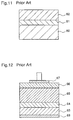
- Figure 11 is a cross-sectional view schematically illustrating one possible structure to produce high quality GaN compounds.
- reference numeral 60 designates a sapphire or SiC substrate
- numeral 61 designates a low temperature GaAlN buffer layer of the chemical composition Ga x Al x-1 N
- numeral 62 designates a GaAlN compound semiconductor layer of the chemical composition Ga x Al x-1 N.
- a low temperature Ga x Al x-1 N (0 ⁇ x ⁇ 1) buffer layer 61 is deposited on the sapphire or SiC substrate 60 at a low temperature in a range from 200°C to 700°C to have a film thickness of 10 nm to 200 nm.
- the low temperature buffer layer 61 is rather amorphous than mono-crystalline.
- the substrate temperature is increased in order to transform the amorphous low temperature buffer layer 61 into a smooth mono-crystalline layer, which is used as a substrate for the following growth of a Ga x Al x-1 N (0 ⁇ x ⁇ 1) compound semiconductor layer 62.
- the compound semiconductor layer 62 is deposited at a temperature in a range from 700°C to 1150°C and exhibits high quality optical and electrical characteristics.
- figure 12 is a cross-sectional view illustrating a semiconductor device in which GaN compound semiconductor layers are grown on an Si substrate, described in US Patent 5,239,188.
- the structure includes a low cost n type Si (111) substrate 63 with a low resistance.
- a low temperature AlN buffer layer 64 is deposited in the common way.
- a high quality n type GaN layer 65 and a p type GaN layer 66 are successively disposed on the low temperature AlN buffer layer 64 at high temperatures.
- Reference numeral 67 designates a p side electrode and numeral 68 designates an n side electrode.
- the Si substrate 65 solves the problems related to the substrate price and the sapphire substrate.
- the lattice mismatch between Si and GaN is as high as about 20%, new problems occur related to the high lattice mismatch. That is, in the structure shown in figure 12, the softest layers remain the GaN layers 65 and 66 and the Si substrate 63, and a high number of dislocations are still observed in the GaN layers 65 and 66. Further, the stress in the Si substrate can lead to the bending of the wafer, which limits the use of this technique drastically.
- a semiconductor device comprises an Si substrate, a stress absorbing layer comprising GaAs and disposed on the Si substrate, a compound buffer layer having a composition of Al x Ga 1-x-y In y N (0 ⁇ x ⁇ 1, 0 ⁇ y ⁇ 1) and disposed on the stress absorbing layer, and a compound semiconductor layer having a composition of Al x Ga 1-x-y In y N (0 ⁇ x ⁇ 1, 0 ⁇ y ⁇ 1) and disposed on the buffer layer. Therefore, the buffer layer protects the GaAs stress absorbing layer from high temperatures during the formation of the compound semiconductor layer, whereby the stress absorbing layer is prevented from decomposition.
- the stress absorbing layer is as thin as 1nm ⁇ 300nm. Therefore, when GaN compounds are grown on the buffer layer, defects in the buffer layer is reduced in a range where the buffer layer is thin, thereby reducing defects in the compound semiconductor layer.
- a semiconductor device comprises an Si substrate, low bonding power layers comprising a material which has a bonding number smaller than that of Si and disposed on regions of the Si substrate, a stress absorbing layer comprising GaAs and disposed on the low bonding power layers and on the Si substrate where the low bonding power layers are not present, and a compound semiconductor layer having a composition of Al x Ga 1-x-y In y N (0 ⁇ x ⁇ 1, 0 ⁇ y ⁇ 1) and disposed on the stress absorbing layer. Therefore, the bonding power between the low bonding power layer having a bonding number smaller than those of the Si substrate and the stress absorbing layer is smaller than the bonding power between the Si substrate and the stress absorbing layer. Further, the stress between the low bonding power layer and the stress absorbing layer is absorbed and the stress between the stress absorbing layer and the Si substrate is reduced. As a result, bending of the Si substrate and generation of cracks in the substrate are suitably prevented.
- a compound buffer layer having a composition of Al x Ga 1-x-y In y N (0 ⁇ x ⁇ 1, 0 ⁇ y ⁇ 1) is disposed on the stress absorbing layer, and a compound semiconductor layer is disposed on the buffer layer. Therefore, the buffer layer protects the stress absorbing layer from high temperatures during the formation of the compound semiconductor layer, whereby the stress absorbing layer is prevented from decomposition.
- the low bonding power layer comprises one selected from the groups consisting of SiO x , SiN x , or SiON, the low bonding power layer is easily formed by oxidizing or nitriding the Si substrate.
- a semiconductor device comprises an Si substrate, a stress absorbing layer comprising As and disposed on the Si substrate, a compound buffer layer having a composition of Al x Ga 1-x-y In y N (0 ⁇ x ⁇ 1, 0 ⁇ y ⁇ 1) and disposed on the stress absorbing layer, and a compound semiconductor layer having a composition of Al x Ga 1-x-y In y N (0 ⁇ x ⁇ 1, 0 ⁇ y ⁇ 1) and disposed on the buffer layer. Therefore, the buffer layer protects the As stress absorbing layer from high temperatures during the formation of the compound semiconductor layer, whereby the stress absorbing layer is prevented from decomposition.
- the Si substrate has a ⁇ 100 ⁇ surface orientation or a ⁇ 111 ⁇ surface orientation. Therefore, when the Si substrate has the ⁇ 100 ⁇ surface, the substrate can be cleaved, on the other hand, when the Si substrate has the ⁇ 111 ⁇ surface, the Si substrate has the same Wurtzite like crystal structure as the nitride buffer layer, whereby crystallinity of the nitride buffer layer is improved.
- the Si substrate, the stress absorbing layer, and the buffer layer comprise impurities for producing conductivity
- the compound semiconductor layer comprises an impurity for producing conductivity and constitutes a light-to-electricity conversion or an electricity-to-light conversion device structure
- the compositions x and y have values corresponding to the device structure. Therefore, the present invention can be applied to the semiconductor laser device, and inexpensive Si substrate is used, resulting in a semiconductor laser device with a low cost.
- the Si substrate can be cleaved and the electrode can be formed on the rear surface of the substrate, additional processing is not required in the fabricating process of the semiconductor laser device, thereby obtaining a semiconductor laser device with a further reduced cost.
- a method of fabricating a semiconductor device comprises preparing an Si substrate, forming a stress absorbing layer comprising one selected from the groups consisting of GaAs or As and having an amorphous or polycrystalline structure on the Si substrate, forming a compound buffer layer having a composition of Al x Ga 1-x-y In y N (0 ⁇ x ⁇ 1, 0 ⁇ y ⁇ 1) on the stress absorbing layer at a temperature such that the stress absorbing layer is not decomposed, partly transforming the stress absorbing layer and the buffer layer, at least a part of the buffer layer, into a monocrystalline structure, and forming a compound semiconductor layer comprising a monocrystalline structure and having a composition of Al x Ga 1-x-y In y N (0 ⁇ x ⁇ 1, 0 ⁇ y ⁇ 1) on the buffer layer which is partly transformed into a monocrystalline structure.
- the buffer layer is grown on the stress absorbing layer without decomposition of the stress absorbing layer and, further, the buffer layer protects the stress absorbing layer from high temperatures during the formation of the compound semiconductor layer, whereby the stress absorbing layer is prevented from decomposition.
- the buffer layer which is formed in amorphous or polycrystalline structure at a low temperature is transformed into a monocrystalline structure, crystallinity of the compound semiconductor layer formed on the buffer layer is improved.
- the stress of the buffer layer is absorbed in the stress absorbing layer during this transformation, dislocations of the compound semiconductor layer formed on the buffer layer are reduced.
- the stress absorbing layer comprises GaAs and is formed at a temperature in a range from 200°C to 600°C. Therefore, the GaAs stress absorbing layer is made amorphous or polycrystalline structure with high stability.
- the stress absorbing layer comprises As and is formed at a temperature in a range from a room temperature to 550°C. Therefore, the As stress absorbing layer is made amorphous or polycrystalline structure with high stability.
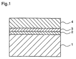
- Figure 1 is a cross-sectional view schematically illustrating a semiconductor device according to a first embodiment of the present invention.
- Figures 2(a)-2(c) are cross-sectional views illustrating process steps in a method of fabricating the semiconductor device according to the first embodiment of the present invention.
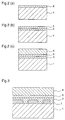
- Figure 3 is a cross-sectional view schematically illustrating a semiconductor device according to a second embodiment of the present invention.
- Figures 4(a)-4(d) are cross-sectional views illustrating process steps in a method of fabricating the semiconductor device according to the second embodiment of the present invention.
- Figure 5 is a cross-sectional view schematically illustrating a semiconductor device according to a third embodiment of the present invention.
- Figure 6 is a cross-sectional view schematically illustrating a semiconductor laser device according to a fourth embodiment of the present invention.
- Figures 7(a)-7(g) are cross-sectional views illustrating process steps in a method of fabricating the semiconductor laser device according to the fourth embodiment of the present invention.
- Figure 8 is a schematic view illustrating typical growth procedures in MOCVD.
- Figure 9 is a schematic view of a high-speed rotating disc MOCVD reactor used for another MOCVD.
- Figure 10 is a schematic view of an MBE chamber for explaining a typical MBE used for the growth of GaN.
- Figure 11 is a cross-sectional view schematically illustrating a semiconductor device in which GaN compound semiconductor layers are grown on a sapphire substrate according to the prior art.
- Figure 12 is a cross-sectional view schematically illustrating a semiconductor device in which GaN compound semiconductor layers are grown on an Si substrate according to the prior art.
- Figure 1 is a cross-sectional view schematically illustrating a semiconductor device according to a first embodiment of the present invention.
- Reference numeral 1 designates an Si substrate.
- a GaAs stress absorbing layer 2 is disposed on the Si substrate 1
- a low temperature GaN buffer layer 3 is disposed on the stress absorbing layer 2
- a GaN compound semiconductor layer 4 is disposed on the low temperature GaN buffer layer 3.
- the GaN compound semiconductor layer 4 is a part of a desired device structure (not shown). That is, on the GaN compound semiconductor layer 4, other GaN compound semiconductor layers are disposed to form the device structure and, further, electrodes (not shown) for the device structure are disposed.
- the Si substrate 1 is desired to have a ⁇ 100 ⁇ surface orientation or a ⁇ 111 ⁇ surface orientation.
- the Si substrate 1 is made to have a ⁇ 100 ⁇ surface orientation.
- the semiconductor device is a device which does not require cleaving of the substrate, since Si and GaAs have never Wurtzite structure, the Si substrate 1 is made to have a ⁇ 111 ⁇ surface orientation so that it has the same Wurtzite like crystal structure as the buffer layer 3, thereby improving the crystallinity of the buffer layer 3 (after recrystallization).
- Figures 2(a)-2(c) are sectional views illustrating process steps in a method of fabricating the semiconductor device according to the first embodiment of the invention.
- the same reference numerals as in figure 1 designate the same or corresponding parts.
- an Si substrate 1 having a ⁇ 100 ⁇ surface orientation is prepared as in the prior art method, and the Si substrate 1 is disposed on a susceptor.
- the Si substrate 1 is cleaned from residual impurities.
- a cleaning method a treatment with atomic hydrogen is used in MBE, and a high temperature process is used in the MOCVD related method.
- a GaAs stress absorbing layer 2 having an amorphous structure is deposited on the Si substrate 1 to a thickness of 1 nm to 300 nm at a substrate temperature in a range from 200°C to 600°C.
- a GaN buffer layer 3 having an amorphous structure is deposited at a substrate temperature in a range from 200°C to 700°C so that the GaAs stress absorbing layer 2 is not decomposed.
- the GaAs stress absorbing layer 2 and the GaN buffer layer 3 may have polycrystalline structures.
- the substrate temperature is raised in order to transform the amorphous GaAs stress absorbing layer 2 and the amorphous GaN buffer layer 3 into monocrystalline layers, that is, in order to recrystallize these layers.
- the recrystallisation is performed at a temperature in a rage from 500°C to 1150°C.
- the crystal structure of the Si substrate forms a template for the crystal structure of the GaAs stress absorbing layer 2
- the crystal structure of the recrystallised GaAs stress absorbing layer forms a template for the crystal structure of the GaN buffer layer 3.
- most of the stress due to lattice mismatch between the Si substrate 1 and the GaN buffer layer 3 is absorbed in the softest layer, that is, the GaAs stress absorbing layer 2.
- the uppermost GaN buffer layer 3 protects the GaAs stress absorbing layer 2 from decomposition.
- a GaN compound semiconductor layer 4 is grown at temperatures above 900°C for the case of MOCVD and the related methods thereof and above 600°C for MBE and the related methods thereof, respectively. Thereafter, other GaN compound semiconductor layers (not shown) are grown to form a desired device structure, and electrodes (not shown) for the device are formed, thereby completing a semiconductor device.
- thermal stress which accumulates, when the Si substrate 1 is cooled down, also should be absorbed in the GaAs stress absorbing layer 2.
- the defects are not prevented from propagating to the GaN layer.
- the GaAs stress absorbing layer 2 with a bulk modulus lower than those of the Si substrate 1 and the GaN compound semiconductor layer 4 is disposed between the Si substrate 1 and the GaN compound semiconductor layer 4, a stress due to lattice mismatch between the Si substrate 1 and the GaN compound semiconductor layer 4 is absorbed in the GaAs stress absorbing layer 2.
- a low cost Si substrate 1 can be used for the GaN series device, whereby price of the GaN series device is significantly reduced.
- the amorphous or polycrystalline GaAs stress absorbing layer 2 is formed on the Si substrate 1 at a low temperature, and the GaN buffer layer 3 is formed on the GaAs stress absorbing layer 2 at a temperature in a range from 200°C to 700°C. Therefore, the GaN buffer layer 3 is formed on the GaAs stress absorbing layer 2 without decomposition of the stress absorbing layer 2. In addition, the GaAs stress absorbing layer 2 is protected from high temperatures during the formation of the compound semiconductor layer 4 and prevented from decomposition.
- the amorphous or polycrystalline GaAs stress absorbing layer 2 and the amorphous or polycrystalline GaN buffer layer 3 which are formed at low temperatures are recrystallized before the growth of the GaN compound semiconductor layer 4, crystallinity of the GaN compound semiconductor layer 4 grown on the GaN buffer layer 3 is improved, and a stress of the GaN buffer layer 3 is absorbed in the stress absorbing layer 2 during the recrystallization, thereby reducing the defects in the compound semiconductor layer 4 formed on the buffer layer 3.
- the GaN buffer layer 3 is recrystallized at a temperature in a range from 500°C, which is a temperature recrystallizing the amorphous or polycrystalline layers, to 1150°C, which is a growth temperature of the GaN compound semiconductor layer 4, the recrystallization of the GaN buffer layer 3 can be suitably performed.
- the GaAs stress absorbing layer 2 is as thin as 1 ⁇ 300 nm, defects in the GaN compound semiconductor layer 4 are significantly reduced.
- the Si substrate has a ⁇ 100 ⁇ surface orientation or a ⁇ 111 ⁇ surface orientation.
- the Si substrate 1 has a ⁇ 100 ⁇ surface
- the substrate can be cleaved
- the Si substrate 1 has a ⁇ 111 ⁇ surface
- the Si substrate has the same Wurtzite like crystal structure as the buffer layer 3, thereby improving the crystallinity of the buffer layer 3 during recrystallization.
- the GaAs stress absorbing layer 2 is formed at a temperature in a range from 200°C to 600°C, the structure of the GaAs stress absorbing layer 2 is made an amorphous or polycrystalline structure with high reliability.
- the GaAs stress absorbing layer 2, the low temperature GaN buffer layer 3, and the GaN compound semiconductor layer 4 are formed on the Si substrate 1 by any of MOCVD, MBE, and CBE, the semiconductor device is suitably fabricated.
- Figure 3 is a cross-sectional view schematically illustrating a semiconductor device according to a second embodiment of the present invention.
- the same reference numerals as in figure 1 designate the same or corresponding parts.
- Reference numeral 7 designates low bonding power layers comprising a dielectric material, such as SiO x , SiN x , and SiON, and disposed in prescribed regions on the Si substrate 1.
- a GaAs stress absorbing layer 2 is disposed on the low bonding power layers 7 and on a region of the Si substrate 1 other than the regions where these layers 7 are present.
- Figures 4(a)-4(d) are cross-sectional views illustrating process steps in a method of fabricating a semiconductor device according to a second embodiment of the invention.
- the same reference numerals as in figures 2(a)-2(c) and figure 3 designate the same or corresponding parts.
- step of figure 4(a) low bonding power layers 7 are formed on the Si substrate 1 by oxidizing or nitriding the Si substrate 1 using a prescribed pattern.
- a stress absorbing layer 2 is formed on the low bonding power layers 7 and the Si substrate 1 and, thereafter, in the steps of figures 4(c) and 4(d), the same process steps as already described with respect to the first embodiment are performed to fabricate the semiconductor device.
- a suitable pattern of the low bonding power layer 7 is of square or circular shape with dimensions of 0.2 ⁇ 2000 ⁇ m, and having a thickness of 10 ⁇ 100 nm.
- the width of the pattern of the low bonding power layer 7 must be such a width that the upper surface of the Si substrate 1 is widely exposed and, whereby the crystal structure of the Si substrate 1 acts as a template for the crystal structure of the GaAs stress absorbing layer 2.
- the material of the low bonding power layer 7 is not restricted to SiO x , SiN x , and SiON. Other materials may be used as long as it has a bonding number smaller than that of Si. However, when SiO x , SiN x , and SiON are used, the low bonding power layers 7 are easily formed on the Si substrate 1 by oxidizing or nitriding the Si substrate 1.
- the low bonding power layers 7 comprising a dielectric material, such as SiO x , SiN x , and SiON, are formed at prescribed regions on the Si substrate 1, and the GaAs stress absorbing layer 2 is formed on the low bonding power layers 7 and on a region of the Si substrate 1 other than the regions where these layers 7 are present.
- a dielectric material such as SiO x , SiN x , and SiON
- the bonding power between the low bonding power layer 7 having a bonding number smaller than those of the Si substrate 1 and the GaAs stress absorbing layer 2 is smaller than the bonding power between the Si substrate 1 and the GaAs stress absorbing layer 2, and the stress between the low bonding power layer 7 and the stress absorbing layer 2 is absorbed and the stress between the stress absorbing layer 2 and the Si substrate 1 is reduced.
- bending of the Si substrate 1 and generation of cracks in the substrate are suitably prevented.
- the GaN buffer layer 3 is formed on the GaAs stress absorbing layer 2 at a low temperature, the GaN buffer layer 3 is formed on the GaAs stress absorbing layer 2 without decomposition of the GaAs stress absorbing layer 2. In addition, the GaAs stress absorbing layer 2 is protected from high temperatures during the formation of the compound semiconductor layer 4 and prevented from decomposition.
- Figure 5 is a cross-sectional view schematically illustrating a semiconductor device according to a third embodiment of the present invention.
- the same reference numerals as in figure 1 designate the same or corresponding parts.
- Reference numeral 122 designates an As stress absorbing layer which is used instead of the GaAs stress absorbing layer 2 shown in figure 1.
- the semiconductor device according to this third embodiment is fabricated as described with respect to the first embodiment, except for the temperature for forming the As stress absorbing layer 122.
- the temperature for forming the As stress absorbing layer 122 is preferably in a range from a room temperature to 550°C so that the structure of the As stress absorbing layer 122 is made an amorphous or polycrystalline structure with high stability.
- the stress absorbing layer As has a bulk modulus lower than those of the Si substrate 1 and the GaN compound semiconductor layer 4, As can be used as the stress absorbing layer as described with respect to GaAs. Further, since As is decomposed at a temperature for growing the GaN compound semiconductor layer 4 as described with respect to GaAs, a GaN buffer layer 3 as a protecting layer is necessary. In addition, since the As stress absorbing layer 122 is excessively soft and unstable when the layer is too thick, the thickness of the As stress absorbing layer 122 is preferably in a range from a few atomic layers to several nanometer.
- the As stress absorbing layer 122, the GaN buffer layer 3, and the GaN compound semiconductor layer 4 are successively formed on the Si substrate 1, the As stress absorbing layer 122 is protected from high temperatures during the formation of the compound semiconductor layer 4 and prevented from decomposition. Therefore, a stress due to lattice mismatch between the Si substrate 1 and the compound semiconductor layer 4 is absorbed in the As stress absorbing layer 122 having the lowest bulk modulus, whereby a compound semiconductor layer 4 with reduced defects is grown on the GaN buffer layer 3, and bending of the Si substrate 1 can be prevented.
- Figure 6 is a cross-sectional view schematically illustrating a semiconductor laser device according to a fourth embodiment of the present invention.
- Reference numeral 101 designates an n type Si substrate.
- An n type GaAs stress absorbing layer 102 is disposed on the n type Si substrate 101.
- a low temperature n type GaN buffer layer 103 is disposed on the n type GaAs stress absorbing layer 102.
- An n type GaN buffer layer 104 is disposed on the low temperature n type GaN buffer layer 103.
- An n type AlGaInN cladding layer 105 is disposed on the n type GaN buffer layer 104.
- An undoped AlGaInN active layer 106 is disposed on the n type AlGaInN cladding layer 105.
- a p type AlGaInN cladding layer 107 is disposed on the undoped AlGaInN active layer 106.
- N type current blocking layers 108 are disposed on regions of the p type AlGaInN cladding layer 107.
- a p side electrode 110 is disposed on the n type current blocking layers 108 and on a region of the p type AlGaInN cladding layer 107 where the n type current blocking layers 108 are not present.
- An n side electrode 109 is disposed on the rear surface of the n type Si substrate 101.
- Figures 7(a)-7(g) are cross-sectional views illustrating process steps in a method of fabricating a semiconductor laser device according to a fourth embodiment of the present invention.
- the same reference numerals as in figure 6 designate the same or corresponding parts.
- the device shown in figure 6 is the semiconductor laser device, it is necessary to cleave the n type Si substrate 101, whereby an n type Si substrate having a ⁇ 100 ⁇ surface orientation is used as the substrate 101.
- the same process steps as described with respect to the first embodiment are performed until the step of disposing the n type GaN buffer layer 104 shown in figure 7(c).
- the n type AlGaInN cladding layer 105, the undoped AlGaInN active layer 106, the p type AlGaInN cladding layer 107, and the n type current blocking layer 108 are successively disposed on the n type GaN buffer layer 104. Thereafter, the prescribed region of the n type current blocking layer 108 is etched and removed and, then the p side electrode 110 is formed on the n type current blocking layers 108 and on a region of the p type AlGaInN cladding layer 107 where the n type current blocking layers 108 are not present and the n side electrode 109 is formed on the rear surface of the n type Si substrate 101, as shown in figure 6. Subsequently, the n type Si substrate 101 is cleaved, thereby completing the semiconductor laser device.
- the Si substrate 101, the GaAs stress absorbing layer 102, and the GaN buffer layer 103 are doped with impurities producing the prescribed conductivity types to make these layers conductive, respectively, and the AlGaInN semiconductor layers 105 to 107, the current blocking layers 108, and the electrodes 109 and 110 are disposed on the GaN buffer layer 103 to form the semiconductor laser structure, whereby the present invention can be applied to the semiconductor laser device. Therefore, an inexpensive Si substrate can be used, thereby obtaining a semiconductor laser device with a low cost. Further, since the Si substrate can be cleaved and the electrode 109 is formed on the rear surface of the substrate, additional processing is not required in the process of fabricating the semiconductor laser device, resulting in a semiconductor laser device with a further reduced cost.
- GaN is used for the compound semiconductor layer 4 and AlGaInN is used for the compound semiconductor layers 105 ⁇ 107, respectively.
- compounds for these layers are not restricted to GaN and AlGaInN. Any compound semiconductor is used as long as the composition is Al x Ga 1-x-y In y N (0 ⁇ x ⁇ 1, 0 ⁇ y ⁇ 1).
- GaN is used for the low temperature buffer layers 3 and 103.
- compounds for these layers are not restricted to GaN. Any compound semiconductor is used as long as the composition is Al x Ga 1-x-y In y N (0 ⁇ x ⁇ 1, 0 ⁇ y ⁇ 1).
- the low temperature buffer layer may have the different composition from those of the compound semiconductor layers.
- the present invention is applied to the semiconductor laser device, the present invention may be applied to a light-to-electricity conversion or an electricity-to-light conversion semiconductor device.
- the GaAs stress absorbing layer 102 is disposed on the Si substrate 101
- low bonding power layers may be disposed at regions on the Si substrate 101 and the GaAs stress absorbing layer 102 may be disposed on the low bonding power layers and a region of the Si substrate 101 where the low bonding power layers are not present.
- the As stress absorbing layer may be provided instead of the GaAs stress absorbing layer 102.
Landscapes
- Recrystallisation Techniques (AREA)
- Led Devices (AREA)
- Physical Deposition Of Substances That Are Components Of Semiconductor Devices (AREA)
- Semiconductor Lasers (AREA)
Applications Claiming Priority (3)
| Application Number | Priority Date | Filing Date | Title |
|---|---|---|---|
| JP32172595A JP3396356B2 (ja) | 1995-12-11 | 1995-12-11 | 半導体装置,及びその製造方法 |
| JP32172595 | 1995-12-11 | ||
| JP321725/95 | 1995-12-11 |
Publications (2)
| Publication Number | Publication Date |
|---|---|
| EP0779666A2 true EP0779666A2 (fr) | 1997-06-18 |
| EP0779666A3 EP0779666A3 (fr) | 2000-03-08 |
Family
ID=18135749
Family Applications (1)
| Application Number | Title | Priority Date | Filing Date |
|---|---|---|---|
| EP96113022A Withdrawn EP0779666A3 (fr) | 1995-12-11 | 1996-08-13 | Dispositif à semi-conducteur et procédé de fabrication |
Country Status (5)
| Country | Link |
|---|---|
| US (1) | US5760426A (fr) |
| EP (1) | EP0779666A3 (fr) |
| JP (1) | JP3396356B2 (fr) |
| KR (1) | KR970052034A (fr) |
| TW (1) | TW307049B (fr) |
Cited By (24)
| Publication number | Priority date | Publication date | Assignee | Title |
|---|---|---|---|---|
| WO1999025030A1 (fr) * | 1997-11-07 | 1999-05-20 | Agilent Technologies, Inc. | Substrat de semiconducteur et procede de fabrication |
| EP1049147A2 (fr) * | 1999-04-28 | 2000-11-02 | Sharp Kabushiki Kaisha | Couche de germanate de plomb fabriquée par croissance épitaxiale |
| EP1054442A3 (fr) * | 1999-05-21 | 2002-04-03 | Toyoda Gosei Co., Ltd. | Procédé de croissance epitaxiale des semi-conducteurs en nitrure du groupe III sur silicium |
| EP1111663A3 (fr) * | 1999-12-20 | 2002-05-02 | Nitride Semiconductors Co., Ltd. | Dispositif semiconducteur composé à base de GaN et procédé de fabrication |
| US6580098B1 (en) | 1999-07-27 | 2003-06-17 | Toyoda Gosei Co., Ltd. | Method for manufacturing gallium nitride compound semiconductor |
| US6610606B2 (en) | 2001-03-27 | 2003-08-26 | Shiro Sakai | Method for manufacturing nitride compound based semiconductor device using an RIE to clean a GaN-based layer |
| US6645295B1 (en) | 1999-05-10 | 2003-11-11 | Toyoda Gosei Co., Ltd. | Method for manufacturing group III nitride compound semiconductor and a light-emitting device using group III nitride compound semiconductor |
| US6844246B2 (en) | 2001-03-22 | 2005-01-18 | Toyoda Gosei Co., Ltd. | Production method of III nitride compound semiconductor, and III nitride compound semiconductor element based on it |
| US6855620B2 (en) | 2000-04-28 | 2005-02-15 | Toyoda Gosei Co., Ltd. | Method for fabricating Group III nitride compound semiconductor substrates and semiconductor devices |
| US6861305B2 (en) | 2000-03-31 | 2005-03-01 | Toyoda Gosei Co., Ltd. | Methods for fabricating group III nitride compound semiconductors and group III nitride compound semiconductor devices |
| US6861270B2 (en) | 2000-06-01 | 2005-03-01 | Shiro Sakai | Method for manufacturing gallium nitride compound semiconductor and light emitting element |
| US6860943B2 (en) | 2001-10-12 | 2005-03-01 | Toyoda Gosei Co., Ltd. | Method for producing group III nitride compound semiconductor |
| US6884647B2 (en) | 2000-09-22 | 2005-04-26 | Shiro Sakai | Method for roughening semiconductor surface |
| EP1032099A3 (fr) * | 1999-02-26 | 2005-11-16 | Matsushita Electric Industrial Co., Ltd. | Dispositif semi-conducteur et procédé de fabrication |
| US6967122B2 (en) | 2000-03-14 | 2005-11-22 | Toyoda Gosei Co., Ltd. | Group III nitride compound semiconductor and method for manufacturing the same |
| US6979584B2 (en) | 1999-12-24 | 2005-12-27 | Toyoda Gosei Co, Ltd. | Method for producing group III nitride compound semiconductor and group III nitride compound semiconductor device |
| US7005685B2 (en) | 2002-02-28 | 2006-02-28 | Shiro Sakai | Gallium-nitride-based compound semiconductor device |
| US7015511B2 (en) | 2001-06-29 | 2006-03-21 | Nitride Semiconductors Co., Ltd. | Gallium nitride-based light emitting device and method for manufacturing the same |
| US7052979B2 (en) | 2001-02-14 | 2006-05-30 | Toyoda Gosei Co., Ltd. | Production method for semiconductor crystal and semiconductor luminous element |
| EP1667228A2 (fr) * | 2004-12-02 | 2006-06-07 | Samsung Electro-Mechanics Co., Ltd | Dispositif semi-conducteur d'émission de la lumière et sa méthode de fabrication |
| US7141444B2 (en) | 2000-03-14 | 2006-11-28 | Toyoda Gosei Co., Ltd. | Production method of III nitride compound semiconductor and III nitride compound semiconductor element |
| US7268371B2 (en) | 1997-06-03 | 2007-09-11 | Philips Lumileds Lighting Company, Llc | Light extraction from a semiconductor light emitting device via chip shaping |
| US7619261B2 (en) | 2000-08-07 | 2009-11-17 | Toyoda Gosei Co., Ltd. | Method for manufacturing gallium nitride compound semiconductor |
| US8461026B2 (en) | 2007-03-23 | 2013-06-11 | Asahi Kasei Emd Corporation | Compound semiconductor lamination, method for manufacturing the same, and semiconductor device |
Families Citing this family (90)
| Publication number | Priority date | Publication date | Assignee | Title |
|---|---|---|---|---|
| CA2258080C (fr) * | 1997-04-11 | 2007-06-05 | Nichia Chemical Industries, Ltd. | Procede assurant la croissance de semi-conducteurs de nitrure, substrat semi-conducteur de nitrure et dispositif semi-conducteur au nitrure. |
| JP3480297B2 (ja) * | 1997-10-10 | 2003-12-15 | 豊田合成株式会社 | 半導体素子 |
| GB2331307A (en) * | 1997-11-15 | 1999-05-19 | Sharp Kk | Growth of buffer layer by molecular beam epitaxy |
| KR100450784B1 (ko) * | 1997-12-12 | 2004-11-16 | 삼성전기주식회사 | Gan단결정제조방법 |
| US6051849A (en) | 1998-02-27 | 2000-04-18 | North Carolina State University | Gallium nitride semiconductor structures including a lateral gallium nitride layer that extends from an underlying gallium nitride layer |
| US6608327B1 (en) * | 1998-02-27 | 2003-08-19 | North Carolina State University | Gallium nitride semiconductor structure including laterally offset patterned layers |
| JPH11274467A (ja) | 1998-03-26 | 1999-10-08 | Murata Mfg Co Ltd | 光電子集積回路素子 |
| US6265289B1 (en) * | 1998-06-10 | 2001-07-24 | North Carolina State University | Methods of fabricating gallium nitride semiconductor layers by lateral growth from sidewalls into trenches, and gallium nitride semiconductor structures fabricated thereby |
| US6344375B1 (en) * | 1998-07-28 | 2002-02-05 | Matsushita Electric Industrial Co., Ltd | Substrate containing compound semiconductor, method for manufacturing the same and semiconductor device using the same |
| US6177688B1 (en) | 1998-11-24 | 2001-01-23 | North Carolina State University | Pendeoepitaxial gallium nitride semiconductor layers on silcon carbide substrates |
| US6255198B1 (en) | 1998-11-24 | 2001-07-03 | North Carolina State University | Methods of fabricating gallium nitride microelectronic layers on silicon layers and gallium nitride microelectronic structures formed thereby |
| US6300590B1 (en) * | 1998-12-16 | 2001-10-09 | General Scanning, Inc. | Laser processing |
| US6521514B1 (en) | 1999-11-17 | 2003-02-18 | North Carolina State University | Pendeoepitaxial methods of fabricating gallium nitride semiconductor layers on sapphire substrates |
| US6380108B1 (en) | 1999-12-21 | 2002-04-30 | North Carolina State University | Pendeoepitaxial methods of fabricating gallium nitride semiconductor layers on weak posts, and gallium nitride semiconductor structures fabricated thereby |
| JP2001185493A (ja) | 1999-12-24 | 2001-07-06 | Toyoda Gosei Co Ltd | Iii族窒化物系化合物半導体の製造方法及びiii族窒化物系化合物半導体素子 |
| US6403451B1 (en) | 2000-02-09 | 2002-06-11 | Noerh Carolina State University | Methods of fabricating gallium nitride semiconductor layers on substrates including non-gallium nitride posts |
| US6392257B1 (en) | 2000-02-10 | 2002-05-21 | Motorola Inc. | Semiconductor structure, semiconductor device, communicating device, integrated circuit, and process for fabricating the same |
| US6693033B2 (en) | 2000-02-10 | 2004-02-17 | Motorola, Inc. | Method of removing an amorphous oxide from a monocrystalline surface |
| US6261929B1 (en) | 2000-02-24 | 2001-07-17 | North Carolina State University | Methods of forming a plurality of semiconductor layers using spaced trench arrays |
| KR20030011083A (ko) | 2000-05-31 | 2003-02-06 | 모토로라 인코포레이티드 | 반도체 디바이스 및 이를 제조하기 위한 방법 |
| WO2002003437A1 (fr) * | 2000-06-30 | 2002-01-10 | Motorola, Inc., A Corporation Of The State Of Delaware | Structure et dispositif de semi-conducteur hybride |
| US6555946B1 (en) | 2000-07-24 | 2003-04-29 | Motorola, Inc. | Acoustic wave device and process for forming the same |
| AU2001277001A1 (en) | 2000-07-24 | 2002-02-05 | Motorola, Inc. | Heterojunction tunneling diodes and process for fabricating same |
| WO2002013245A1 (fr) | 2000-08-04 | 2002-02-14 | The Regents Of The University Of California | Procede pour reguler les contraintes dans des films de nitrure de gallium deposes sur des substrats |
| US6638838B1 (en) | 2000-10-02 | 2003-10-28 | Motorola, Inc. | Semiconductor structure including a partially annealed layer and method of forming the same |
| US6649287B2 (en) * | 2000-12-14 | 2003-11-18 | Nitronex Corporation | Gallium nitride materials and methods |
| US20020096683A1 (en) | 2001-01-19 | 2002-07-25 | Motorola, Inc. | Structure and method for fabricating GaN devices utilizing the formation of a compliant substrate |
| US7233028B2 (en) * | 2001-02-23 | 2007-06-19 | Nitronex Corporation | Gallium nitride material devices and methods of forming the same |
| US6956250B2 (en) | 2001-02-23 | 2005-10-18 | Nitronex Corporation | Gallium nitride materials including thermally conductive regions |
| US6611002B2 (en) | 2001-02-23 | 2003-08-26 | Nitronex Corporation | Gallium nitride material devices and methods including backside vias |
| US6673646B2 (en) | 2001-02-28 | 2004-01-06 | Motorola, Inc. | Growth of compound semiconductor structures on patterned oxide films and process for fabricating same |
| WO2002082551A1 (fr) | 2001-04-02 | 2002-10-17 | Motorola, Inc. | Structure de semi-conducteur a courant de fuite attenue |
| US20040029365A1 (en) * | 2001-05-07 | 2004-02-12 | Linthicum Kevin J. | Methods of fabricating gallium nitride microelectronic layers on silicon layers and gallium nitride microelectronic structures formed thereby |
| US6709989B2 (en) | 2001-06-21 | 2004-03-23 | Motorola, Inc. | Method for fabricating a semiconductor structure including a metal oxide interface with silicon |
| US6992321B2 (en) | 2001-07-13 | 2006-01-31 | Motorola, Inc. | Structure and method for fabricating semiconductor structures and devices utilizing piezoelectric materials |
| US6646293B2 (en) | 2001-07-18 | 2003-11-11 | Motorola, Inc. | Structure for fabricating high electron mobility transistors utilizing the formation of complaint substrates |
| US6693298B2 (en) | 2001-07-20 | 2004-02-17 | Motorola, Inc. | Structure and method for fabricating epitaxial semiconductor on insulator (SOI) structures and devices utilizing the formation of a compliant substrate for materials used to form same |
| US7019332B2 (en) | 2001-07-20 | 2006-03-28 | Freescale Semiconductor, Inc. | Fabrication of a wavelength locker within a semiconductor structure |
| US6855992B2 (en) | 2001-07-24 | 2005-02-15 | Motorola Inc. | Structure and method for fabricating configurable transistor devices utilizing the formation of a compliant substrate for materials used to form the same |
| US6667196B2 (en) | 2001-07-25 | 2003-12-23 | Motorola, Inc. | Method for real-time monitoring and controlling perovskite oxide film growth and semiconductor structure formed using the method |
| US6639249B2 (en) | 2001-08-06 | 2003-10-28 | Motorola, Inc. | Structure and method for fabrication for a solid-state lighting device |
| US6589856B2 (en) | 2001-08-06 | 2003-07-08 | Motorola, Inc. | Method and apparatus for controlling anti-phase domains in semiconductor structures and devices |
| US20030034491A1 (en) | 2001-08-14 | 2003-02-20 | Motorola, Inc. | Structure and method for fabricating semiconductor structures and devices for detecting an object |
| US6673667B2 (en) | 2001-08-15 | 2004-01-06 | Motorola, Inc. | Method for manufacturing a substantially integral monolithic apparatus including a plurality of semiconductor materials |
| US20030071327A1 (en) | 2001-10-17 | 2003-04-17 | Motorola, Inc. | Method and apparatus utilizing monocrystalline insulator |
| US6916717B2 (en) | 2002-05-03 | 2005-07-12 | Motorola, Inc. | Method for growing a monocrystalline oxide layer and for fabricating a semiconductor device on a monocrystalline substrate |
| TW574762B (en) * | 2002-10-16 | 2004-02-01 | Univ Nat Cheng Kung | Method for growing monocrystal GaN on silicon substrate |
| US7169619B2 (en) | 2002-11-19 | 2007-01-30 | Freescale Semiconductor, Inc. | Method for fabricating semiconductor structures on vicinal substrates using a low temperature, low pressure, alkaline earth metal-rich process |
| US6885065B2 (en) | 2002-11-20 | 2005-04-26 | Freescale Semiconductor, Inc. | Ferromagnetic semiconductor structure and method for forming the same |
| US7020374B2 (en) | 2003-02-03 | 2006-03-28 | Freescale Semiconductor, Inc. | Optical waveguide structure and method for fabricating the same |
| US6965128B2 (en) | 2003-02-03 | 2005-11-15 | Freescale Semiconductor, Inc. | Structure and method for fabricating semiconductor microresonator devices |
| EP1617464A4 (fr) * | 2003-03-19 | 2011-04-27 | Japan Science & Tech Agency | Procede permettant de faire croitre du cristal semi-conducteur |
| TWI240969B (en) * | 2003-06-06 | 2005-10-01 | Sanken Electric Co Ltd | Nitride semiconductor device and method for manufacturing same |
| WO2005060007A1 (fr) * | 2003-08-05 | 2005-06-30 | Nitronex Corporation | Transistors a base de nitrure de gallium et procedes associes |
| JP2005093682A (ja) * | 2003-09-17 | 2005-04-07 | Toyoda Gosei Co Ltd | GaN系半導体発光素子及びその製造方法 |
| US7071498B2 (en) * | 2003-12-17 | 2006-07-04 | Nitronex Corporation | Gallium nitride material devices including an electrode-defining layer and methods of forming the same |
| US20050145851A1 (en) * | 2003-12-17 | 2005-07-07 | Nitronex Corporation | Gallium nitride material structures including isolation regions and methods |
| US7361946B2 (en) * | 2004-06-28 | 2008-04-22 | Nitronex Corporation | Semiconductor device-based sensors |
| US7339205B2 (en) * | 2004-06-28 | 2008-03-04 | Nitronex Corporation | Gallium nitride materials and methods associated with the same |
| US7687827B2 (en) * | 2004-07-07 | 2010-03-30 | Nitronex Corporation | III-nitride materials including low dislocation densities and methods associated with the same |
| EP1831919A2 (fr) * | 2004-10-28 | 2007-09-12 | Nitronex Corporation | Circuits integres monolithiques hyperfrequences a base de nitrure de gallium |
| US7247889B2 (en) | 2004-12-03 | 2007-07-24 | Nitronex Corporation | III-nitride material structures including silicon substrates |
| US7365374B2 (en) * | 2005-05-03 | 2008-04-29 | Nitronex Corporation | Gallium nitride material structures including substrates and methods associated with the same |
| JP2007042857A (ja) * | 2005-08-03 | 2007-02-15 | Nichia Chem Ind Ltd | 半導体発光素子と半導体素子の製造方法及び半導体発光装置 |
| KR20080072833A (ko) * | 2005-10-04 | 2008-08-07 | 니트로넥스 코오포레이션 | 광대역 애플리케이션을 위한 갈륨 나이트라이드 물질트랜지스터 및 방법 |
| CN101326646B (zh) * | 2005-11-01 | 2011-03-16 | 麻省理工学院 | 单片集成的半导体材料和器件 |
| EP1969635B1 (fr) * | 2005-12-02 | 2017-07-19 | Infineon Technologies Americas Corp. | Dispositifs en matériaux au nitrure de gallium et procédés associés |
| US7566913B2 (en) | 2005-12-02 | 2009-07-28 | Nitronex Corporation | Gallium nitride material devices including conductive regions and methods associated with the same |
| WO2008021451A2 (fr) * | 2006-08-14 | 2008-02-21 | Aktiv-Dry Llc | Inhalateur à poudre sèche actionné par l'homme et compositions à inhaler sous forme de poudre sèche |
| US7825432B2 (en) | 2007-03-09 | 2010-11-02 | Cree, Inc. | Nitride semiconductor structures with interlayer structures |
| US8362503B2 (en) | 2007-03-09 | 2013-01-29 | Cree, Inc. | Thick nitride semiconductor structures with interlayer structures |
| US7745848B1 (en) | 2007-08-15 | 2010-06-29 | Nitronex Corporation | Gallium nitride material devices and thermal designs thereof |
| US8026581B2 (en) * | 2008-02-05 | 2011-09-27 | International Rectifier Corporation | Gallium nitride material devices including diamond regions and methods associated with the same |
| US8343824B2 (en) * | 2008-04-29 | 2013-01-01 | International Rectifier Corporation | Gallium nitride material processing and related device structures |
| JP5272160B2 (ja) * | 2008-09-19 | 2013-08-28 | 旭化成エレクトロニクス株式会社 | 化合物半導体積層体及び半導体デバイス |
| US8299351B2 (en) * | 2009-02-24 | 2012-10-30 | Hong Kong Applied Science And Technology Research Institute Co., Ltd. | Epitaxial growth of III-V compounds on (111) silicon for solar cells |
| KR100999684B1 (ko) * | 2009-10-21 | 2010-12-08 | 엘지이노텍 주식회사 | 발광 소자 및 그 제조방법 |
| US9312436B2 (en) | 2011-05-16 | 2016-04-12 | Kabushiki Kaisha Toshiba | Nitride semiconductor device, nitride semiconductor wafer, and method for manufacturing nitride semiconductor layer |
| KR101547546B1 (ko) * | 2013-09-17 | 2015-08-28 | 서울대학교산학협력단 | 박막 구조체 및 그 제조방법 |
| US9704705B2 (en) | 2015-09-08 | 2017-07-11 | Macom Technology Solutions Holdings, Inc. | Parasitic channel mitigation via reaction with active species |
| US9773898B2 (en) | 2015-09-08 | 2017-09-26 | Macom Technology Solutions Holdings, Inc. | III-nitride semiconductor structures comprising spatially patterned implanted species |
| US9799520B2 (en) | 2015-09-08 | 2017-10-24 | Macom Technology Solutions Holdings, Inc. | Parasitic channel mitigation via back side implantation |
| US10211294B2 (en) | 2015-09-08 | 2019-02-19 | Macom Technology Solutions Holdings, Inc. | III-nitride semiconductor structures comprising low atomic mass species |
| US9806182B2 (en) | 2015-09-08 | 2017-10-31 | Macom Technology Solutions Holdings, Inc. | Parasitic channel mitigation using elemental diboride diffusion barrier regions |
| US20170069721A1 (en) | 2015-09-08 | 2017-03-09 | M/A-Com Technology Solutions Holdings, Inc. | Parasitic channel mitigation using silicon carbide diffusion barrier regions |
| US9627473B2 (en) | 2015-09-08 | 2017-04-18 | Macom Technology Solutions Holdings, Inc. | Parasitic channel mitigation in III-nitride material semiconductor structures |
| US9673281B2 (en) | 2015-09-08 | 2017-06-06 | Macom Technology Solutions Holdings, Inc. | Parasitic channel mitigation using rare-earth oxide and/or rare-earth nitride diffusion barrier regions |
| US9960127B2 (en) | 2016-05-18 | 2018-05-01 | Macom Technology Solutions Holdings, Inc. | High-power amplifier package |
| US10134658B2 (en) | 2016-08-10 | 2018-11-20 | Macom Technology Solutions Holdings, Inc. | High power transistors |
| US11038023B2 (en) | 2018-07-19 | 2021-06-15 | Macom Technology Solutions Holdings, Inc. | III-nitride material semiconductor structures on conductive silicon substrates |
Family Cites Families (2)
| Publication number | Priority date | Publication date | Assignee | Title |
|---|---|---|---|---|
| US5290393A (en) * | 1991-01-31 | 1994-03-01 | Nichia Kagaku Kogyo K.K. | Crystal growth method for gallium nitride-based compound semiconductor |
| JP3352712B2 (ja) * | 1991-12-18 | 2002-12-03 | 浩 天野 | 窒化ガリウム系半導体素子及びその製造方法 |
-
1995
- 1995-12-11 JP JP32172595A patent/JP3396356B2/ja not_active Expired - Fee Related
-
1996
- 1996-03-04 TW TW085102598A patent/TW307049B/zh not_active IP Right Cessation
- 1996-07-16 US US08/680,850 patent/US5760426A/en not_active Expired - Lifetime
- 1996-08-13 EP EP96113022A patent/EP0779666A3/fr not_active Withdrawn
- 1996-12-06 KR KR1019960062361A patent/KR970052034A/ko not_active Withdrawn
Cited By (37)
| Publication number | Priority date | Publication date | Assignee | Title |
|---|---|---|---|---|
| US7268371B2 (en) | 1997-06-03 | 2007-09-11 | Philips Lumileds Lighting Company, Llc | Light extraction from a semiconductor light emitting device via chip shaping |
| WO1999025030A1 (fr) * | 1997-11-07 | 1999-05-20 | Agilent Technologies, Inc. | Substrat de semiconducteur et procede de fabrication |
| US6537513B1 (en) | 1997-11-07 | 2003-03-25 | Lumileds Lighting U.S., Llc | Semiconductor substrate and method for making the same |
| EP1032099A3 (fr) * | 1999-02-26 | 2005-11-16 | Matsushita Electric Industrial Co., Ltd. | Dispositif semi-conducteur et procédé de fabrication |
| EP1049147A2 (fr) * | 1999-04-28 | 2000-11-02 | Sharp Kabushiki Kaisha | Couche de germanate de plomb fabriquée par croissance épitaxiale |
| US6645295B1 (en) | 1999-05-10 | 2003-11-11 | Toyoda Gosei Co., Ltd. | Method for manufacturing group III nitride compound semiconductor and a light-emitting device using group III nitride compound semiconductor |
| US6881651B2 (en) | 1999-05-21 | 2005-04-19 | Toyoda Gosei Co., Ltd. | Methods and devices using group III nitride compound semiconductor |
| EP1054442A3 (fr) * | 1999-05-21 | 2002-04-03 | Toyoda Gosei Co., Ltd. | Procédé de croissance epitaxiale des semi-conducteurs en nitrure du groupe III sur silicium |
| US6617668B1 (en) | 1999-05-21 | 2003-09-09 | Toyoda Gosei Co., Ltd. | Methods and devices using group III nitride compound semiconductor |
| US7176497B2 (en) | 1999-07-27 | 2007-02-13 | Toyoda Gosei Co., Ltd. | Group III nitride compound semiconductor |
| US6893945B2 (en) | 1999-07-27 | 2005-05-17 | Toyoda Gosei Co., Ltd. | Method for manufacturing gallium nitride group compound semiconductor |
| US6818926B2 (en) | 1999-07-27 | 2004-11-16 | Toyoda Gosei Co., Ltd. | Method for manufacturing gallium nitride compound semiconductor |
| US6835966B2 (en) | 1999-07-27 | 2004-12-28 | Toyoda Gosei Co., Ltd. | Method for manufacturing gallium nitride compound semiconductor |
| US6580098B1 (en) | 1999-07-27 | 2003-06-17 | Toyoda Gosei Co., Ltd. | Method for manufacturing gallium nitride compound semiconductor |
| US6930329B2 (en) | 1999-07-27 | 2005-08-16 | Toyoda Gosei Co., Ltd. | Method for manufacturing gallium nitride compound semiconductor |
| EP1111663A3 (fr) * | 1999-12-20 | 2002-05-02 | Nitride Semiconductors Co., Ltd. | Dispositif semiconducteur composé à base de GaN et procédé de fabrication |
| KR100453210B1 (ko) * | 1999-12-20 | 2004-10-15 | 나이트라이드 세마이컨덕터스 코포레이션, 리미티드 | GaN계 화합물 반도체의 제조 방법과 GaN계 화합물반도체 디바이스 |
| US6475882B1 (en) | 1999-12-20 | 2002-11-05 | Nitride Semiconductors Co., Ltd. | Method for producing GaN-based compound semiconductor and GaN-based compound semiconductor device |
| US7560725B2 (en) | 1999-12-24 | 2009-07-14 | Toyoda Gosei Co., Ltd. | Method for fabricating group III nitride compound semiconductors and group III nitride compound semiconductor devices |
| US6979584B2 (en) | 1999-12-24 | 2005-12-27 | Toyoda Gosei Co, Ltd. | Method for producing group III nitride compound semiconductor and group III nitride compound semiconductor device |
| US7462867B2 (en) | 2000-03-14 | 2008-12-09 | Toyoda Gosei Co., Ltd. | Group III nitride compound semiconductor devices and method for fabricating the same |
| US7141444B2 (en) | 2000-03-14 | 2006-11-28 | Toyoda Gosei Co., Ltd. | Production method of III nitride compound semiconductor and III nitride compound semiconductor element |
| US6967122B2 (en) | 2000-03-14 | 2005-11-22 | Toyoda Gosei Co., Ltd. | Group III nitride compound semiconductor and method for manufacturing the same |
| US6861305B2 (en) | 2000-03-31 | 2005-03-01 | Toyoda Gosei Co., Ltd. | Methods for fabricating group III nitride compound semiconductors and group III nitride compound semiconductor devices |
| US7491984B2 (en) | 2000-03-31 | 2009-02-17 | Toyoda Gosei Co., Ltd. | Method for fabricating group III nitride compound semiconductors and group III nitride compound semiconductor devices |
| US6855620B2 (en) | 2000-04-28 | 2005-02-15 | Toyoda Gosei Co., Ltd. | Method for fabricating Group III nitride compound semiconductor substrates and semiconductor devices |
| US6861270B2 (en) | 2000-06-01 | 2005-03-01 | Shiro Sakai | Method for manufacturing gallium nitride compound semiconductor and light emitting element |
| US7619261B2 (en) | 2000-08-07 | 2009-11-17 | Toyoda Gosei Co., Ltd. | Method for manufacturing gallium nitride compound semiconductor |
| US6884647B2 (en) | 2000-09-22 | 2005-04-26 | Shiro Sakai | Method for roughening semiconductor surface |
| US7052979B2 (en) | 2001-02-14 | 2006-05-30 | Toyoda Gosei Co., Ltd. | Production method for semiconductor crystal and semiconductor luminous element |
| US6844246B2 (en) | 2001-03-22 | 2005-01-18 | Toyoda Gosei Co., Ltd. | Production method of III nitride compound semiconductor, and III nitride compound semiconductor element based on it |
| US6610606B2 (en) | 2001-03-27 | 2003-08-26 | Shiro Sakai | Method for manufacturing nitride compound based semiconductor device using an RIE to clean a GaN-based layer |
| US7015511B2 (en) | 2001-06-29 | 2006-03-21 | Nitride Semiconductors Co., Ltd. | Gallium nitride-based light emitting device and method for manufacturing the same |
| US6860943B2 (en) | 2001-10-12 | 2005-03-01 | Toyoda Gosei Co., Ltd. | Method for producing group III nitride compound semiconductor |
| US7005685B2 (en) | 2002-02-28 | 2006-02-28 | Shiro Sakai | Gallium-nitride-based compound semiconductor device |
| EP1667228A2 (fr) * | 2004-12-02 | 2006-06-07 | Samsung Electro-Mechanics Co., Ltd | Dispositif semi-conducteur d'émission de la lumière et sa méthode de fabrication |
| US8461026B2 (en) | 2007-03-23 | 2013-06-11 | Asahi Kasei Emd Corporation | Compound semiconductor lamination, method for manufacturing the same, and semiconductor device |
Also Published As
| Publication number | Publication date |
|---|---|
| EP0779666A3 (fr) | 2000-03-08 |
| US5760426A (en) | 1998-06-02 |
| TW307049B (en) | 1997-06-01 |
| KR970052034A (ko) | 1997-07-29 |
| JP3396356B2 (ja) | 2003-04-14 |
| JPH09162125A (ja) | 1997-06-20 |
Similar Documents
| Publication | Publication Date | Title |
|---|---|---|
| US5760426A (en) | Heteroepitaxial semiconductor device including silicon substrate, GaAs layer and GaN layer #13 | |
| EP0342937B1 (fr) | Fabrication d'une plaquette semi-conductrice ayant une couche d'un composé semi-conducteur du groupe III-V sur un substrat en silicium | |
| EP1997125B1 (fr) | Procédé de croissance au moyen de couches conformes nanocolonaires et de hvpe pour la production de matériaux semi-conducteurs composés de haute qualité | |
| EP0331467B1 (fr) | Méthode pour former une couche mince semi-conductrice | |
| EP1246233B1 (fr) | Procédé de fabrication d'un substrat semiconducteur de GaN | |
| JP3093904B2 (ja) | 化合物半導体結晶の成長方法 | |
| US6176925B1 (en) | Detached and inverted epitaxial regrowth & methods | |
| JP2006523033A (ja) | シリコン上に単結晶GaNを成長させる方法 | |
| KR20100092932A (ko) | 반도체 기판 및 반도체 기판의 제조 방법 | |
| EP1298709B1 (fr) | Procede de fabrication d'un element en nitrure du group iii comprenant substrat epitaxial pour element en nitrure de groupe iii | |
| US7968438B2 (en) | Ultra-thin high-quality germanium on silicon by low-temperature epitaxy and insulator-capped annealing | |
| US6255004B1 (en) | III-V nitride semiconductor devices and process for the production thereof | |
| EP0430562B1 (fr) | Hétérostructure semi-conductrice et méthode pour sa fabrication | |
| US6339014B1 (en) | Method for growing nitride compound semiconductor | |
| KR100450781B1 (ko) | Gan단결정제조방법 | |
| EP0241204B1 (fr) | Méthode pour former une couche cristalline déposée | |
| US7361522B2 (en) | Growing lower defect semiconductor crystals on highly lattice-mismatched substrates | |
| KR100699739B1 (ko) | Ⅲ-ⅴ족 화합물 반도체 | |
| US20030027407A1 (en) | Method for producing group III nitride compound semiconductor | |
| KR100682272B1 (ko) | 질화물계 기판 제조 방법 및 이에 따른 질화물계 기판 | |
| JP2005136200A (ja) | 窒化物半導体結晶層の作製方法、窒化物半導体結晶層、及び窒化物半導体結晶層作製用の基材 | |
| US5281551A (en) | Method for delta-doping in GaAs epitaxial layer grown on silicon substrate by metalorganic chemical vapor deposition | |
| US6844574B1 (en) | III-V compound semiconductor | |
| KR100643155B1 (ko) | 실리콘 기판-단결정 GaN 박막 적층체의 제조방법 | |
| KR100450784B1 (ko) | Gan단결정제조방법 |
Legal Events
| Date | Code | Title | Description |
|---|---|---|---|
| PUAI | Public reference made under article 153(3) epc to a published international application that has entered the european phase |
Free format text: ORIGINAL CODE: 0009012 |
|
| AK | Designated contracting states |
Kind code of ref document: A2 Designated state(s): DE FR GB |
|
| PUAL | Search report despatched |
Free format text: ORIGINAL CODE: 0009013 |
|
| AK | Designated contracting states |
Kind code of ref document: A3 Designated state(s): DE FR GB |
|
| RIC1 | Information provided on ipc code assigned before grant |
Free format text: 7H 01L 33/00 A, 7H 01L 29/201 B, 7H 01S 3/19 B |
|
| STAA | Information on the status of an ep patent application or granted ep patent |
Free format text: STATUS: THE APPLICATION IS DEEMED TO BE WITHDRAWN |
|
| 18D | Application deemed to be withdrawn |
Effective date: 20000201 |