EP0780035B1 - Oscillateur rc precis - Google Patents
Oscillateur rc precis Download PDFInfo
- Publication number
- EP0780035B1 EP0780035B1 EP96925272A EP96925272A EP0780035B1 EP 0780035 B1 EP0780035 B1 EP 0780035B1 EP 96925272 A EP96925272 A EP 96925272A EP 96925272 A EP96925272 A EP 96925272A EP 0780035 B1 EP0780035 B1 EP 0780035B1
- Authority
- EP
- European Patent Office
- Prior art keywords
- voltage
- coupled
- flip flop
- oscillatory signal
- circuit
- Prior art date
- Legal status (The legal status is an assumption and is not a legal conclusion. Google has not performed a legal analysis and makes no representation as to the accuracy of the status listed.)
- Expired - Lifetime
Links
- 230000003534 oscillatory effect Effects 0.000 claims description 55
- 239000003990 capacitor Substances 0.000 claims description 54
- 230000010355 oscillation Effects 0.000 claims description 10
- 238000005070 sampling Methods 0.000 claims description 8
- 238000007599 discharging Methods 0.000 claims description 6
- 238000000034 method Methods 0.000 claims description 6
- 239000004065 semiconductor Substances 0.000 claims description 2
- 230000000063 preceeding effect Effects 0.000 claims 1
- 238000010586 diagram Methods 0.000 description 5
- 230000008859 change Effects 0.000 description 3
- 230000004044 response Effects 0.000 description 3
- 238000001514 detection method Methods 0.000 description 1
- 230000000694 effects Effects 0.000 description 1
- 230000006870 function Effects 0.000 description 1
- 239000000463 material Substances 0.000 description 1
- 238000012986 modification Methods 0.000 description 1
- 230000004048 modification Effects 0.000 description 1
- 230000008569 process Effects 0.000 description 1
- 239000010409 thin film Substances 0.000 description 1
- 230000007704 transition Effects 0.000 description 1
- 230000010356 wave oscillation Effects 0.000 description 1
Images

Classifications
-
- H—ELECTRICITY
- H03—ELECTRONIC CIRCUITRY
- H03K—PULSE TECHNIQUE
- H03K3/00—Circuits for generating electric pulses; Monostable, bistable or multistable circuits
- H03K3/02—Generators characterised by the type of circuit or by the means used for producing pulses
- H03K3/023—Generators characterised by the type of circuit or by the means used for producing pulses by the use of differential amplifiers or comparators, with internal or external positive feedback
- H03K3/0231—Astable circuits
-
- H—ELECTRICITY
- H03—ELECTRONIC CIRCUITRY
- H03K—PULSE TECHNIQUE
- H03K3/00—Circuits for generating electric pulses; Monostable, bistable or multistable circuits
- H03K3/01—Details
- H03K3/011—Modifications of generator to compensate for variations in physical values, e.g. voltage, temperature
Definitions
- This invention generally relates to oscillator circuits and, in particular, to an RC oscillator circuit for oscillating at a predetermined frequency by accurately oscillating between two precise voltage levels and having negligible temperature or power supply variation effects.
- Oscillator circuits are used in a myriad of applications in the electronics industry for providing clock and other timing signals to electronic circuitry such as microprocessors, microcontrollers, flip-flop circuits, latch circuits, etc.
- RC oscillator circuits typically include a control circuit coupled to the interconnection between a series resistor-capacitor (RC) network. The control circuit alternately charges or discharges the voltage across the capacitor through the resistor to generate an oscillatory signal appearing across the capacitor. The frequency of oscillation is determined by the time constant of the resistor and capacitor.
- the 555 timer includes a set/reset (SR) flip-flop and first and second comparators.
- the interconnection between the series RC network is coupled to one input of each of the comparators.
- the other input of the first comparator is coupled to receive a high threshold voltage (V H ) while the other input of the second comparator is coupled to receive a low threshold voltage (V L ).
- the output of first comparator is coupled to the set input of the flip-flop while the output of the second comparator is coupled to the reset input of the flip-flop.
- An output of the flip-flop is coupled to the resistor of the RC network.
- the first comparator sets the flip-flop, which commences the discharging of the voltage across the capacitor, when the RC oscillatory signal exceeds the predetermined high threshold voltage, and the second comparator resets the flip-flop, which commences the charging of the voltage across the capacitor, when the RC oscillatory signal falls below the predetermined low threshold voltage.
- the signal appearing across the capacitor approximately oscillates between the high and low threshold voltages at a frequency determined by the value of the resistor and capacitor of the RC network.
- U.S. Patent No. 4,122,413 to Chen discloses a single pin MOS RC oscillator circuit for oscillating between two threshold levels whose difference remains substantially constant.
- the RC oscillator circuit includes an external resistor and capacitor connected in series across power supply terminals of an integrated circuit (IC).
- the IC controls the charging and discharging of the capacitor.
- the IC is connected to the interconnection of the resistor and capacitor, and includes an MOS switch which is coupled across the capacitor. When the switch is on, the voltage across the capacitor will discharge through the resistor, and when the switch is off, the capacitor is charged through the resistor.
- the IC also includes a pair of inverters having similar but different threshold values, coupled between the resistor and capacitor.
- Logic circuitry of the IC is coupled to the pair of inverters and configured such that the switch is "off” as long as the capacitor voltage is below the threshold of both inverters, but the switch is "on” when the capacitor voltage exceeds both thresholds. Accordingly, the Chen '413 patent teaches that the voltage across the capacitor will oscillate between the two threshold voltages of the inverters at a frequency set by the RC time constant of the RC network. However, as stated in the Chen '413 patent, the threshold voltages of the inverters are not precise and will vary. However, the threshold voltages will vary in the same direction so that the difference between the threshold voltages will remain substantially constant. Accordingly, the frequency of oscillation remains substantially constant.
- the present invention provides a circuit for generating an oscillatory signal of a predetermined frequency across a network by ensuring that the oscillatory signal accurately oscillates between first and second voltage generated from a first supply voltage source and where the frequency of oscillation is determined by the time constant of the network.
- the circuit includes first and second comparators having their outputs respectively coupled to first and second inputs of a flip flop for setting and resetting the flip flop, an output of the flip flop being coupled to the network for controlling the charging and discharging of the voltage across capacitor.
- the interconnection of the network is coupled to an input of both the first and second comparators.
- the circuit according to the invention comprises a first voltage modifying circuit for receiving the first voltage and for applying a modified version of the first voltage to the other input of the first comparator such that the first comparator switches before the oscillatory signal actually reaches the first voltage, thereby ensuring that the oscillatory signal precisely reaches the first voltage by the time the flip flop switches.
- This circuit further includes a second voltage modifying circuit for receiving the second voltage and for applying a modified version of the second voltage to the other input of the second comparator such that the second comparator switches before the oscillatory signal actually reaches the second voltage thereby ensuring that the oscillatory signal precisely reaches the second voltage by the time the flip flop switches.
- the invention is characterized in that the network is a series resistor-capacitor network and the first voltage modifying circuit includes first means for sampling the oscillatory signal upon switching of the flip flop from a first logic level to a second logic level, said second voltage modifying circuit further including second means for sampling the oscillatory signal upon switching of the flip flop from a second logic level to a first logic level, the sampling of the oscillatory signal being controlled by an output signal of said flip flop.
- Another object of the present invention is to modify the voltage high and voltage low threshold values of a conventional 555 timer corresponding to the voltage level of the oscillatory signal when the flip-flop switches thereby ensuring that the oscillatory signal accurately oscillates at a precise frequency by accurately oscillating between precise voltage levels.
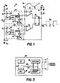
- RC oscillator circuit 10 for generating an oscillatory signal of a predetermined frequency by accurately oscillating between precise predetermined voltage levels, for example, predetermined high and low voltage thresholds.
- Oscillator circuit 10 generates an oscillatory signal at circuit node 12 (i.e., across capacitor 14), that accurately oscillates between low and high threshold voltage values.
- the frequency of oscillation is determined by the time constant of the resistor (22) and the capacitor (14) wherein the frequency of oscillation is inversely proportional to the product of R 22 and C 14 as will be shown hereinafter.
- Oscillator circuit 10 includes comparators 16 and 18 and S/R flip flop 20 all of which comprise the components of a conventional 555 timer. Comparators 16 and 18 have outputs respectively coupled to the set and reset inputs of SR flip-flop 20. Circuit node 12, which the interconnection of the RC network comprised of capacitor 14 and resistor 22, is coupled to the non-inverting input of comparator 16 and the inverting input of comparator 18. The inverting input of comparator 16 is coupled to receive a modified version of the high threshold voltage (V H ), as represented by V' H . Likewise, the non-inverting input of comparator 18 is coupled to receive a modified version of the low threshold voltage (V L ) as represented by V' L .
- V H high threshold voltage
- V L low threshold voltage
- An inverting output of flip-flop 20 is coupled through resistor 22 to circuit node 12.
- the output of flip-flop 20 switches between the supply voltages applied to flip-flop 20, for example, between voltages V DD and V SS , depending on whether the flip-flop is being set or reset. For example, when flip-flop 20 is set, the inverting output of flip-flop 20 switches from a logic 1 to a logic 0 and, thus, transitions from voltage V DD to voltage V SS .
- Oscillator circuit 10 further includes voltage modifying circuits 24 and 25 for respectively generating modified high and low threshold voltages applied to comparators 16 and 18 based upon the overshoot (of voltage V H ) or undershoot (of voltage V L ) of the oscillatory signal appearing at circuit node 12 when flip flop 20 switches.
- circuit 24 generates and applies a modified voltage V' H to the inverting input of comparator 16 so that by the time flip flop 20 actually switches in response to the oscillatory signal exceeding modified voltage V' H , the oscillatory signal is substantially equal to the predetermined high threshold voltage V H .
- circuit 25 generates and applies a modified voltage V' L to the inverting input of comparator 18 so that by the time flip flop 20 actually switches in response to the oscillatory signal falling below modified voltage V' L , the oscillatory signal is substantially equal to the predetermined low threshold voltage V L .
- the present invention provides a signal appearing at circuit node 12 that accurately oscillates between voltages V L and V H . This ensures that the signal at circuit node 12 oscillates at a predetermined and substantially constant frequency.
- Voltage modifying circuit 24 includes amplifier 26 for generating and applying a modified version of the high threshold voltage to comparator 16.
- Amplifier 26 has a first input coupled to receive high threshold voltage V H .
- the second input of amplifier 26 is coupled to a first terminal of capacitor 28, the latter having a second terminal coupled to the output of amplifier 26.
- the output of amplifier 26 is further coupled to the inverting input of comparator 16.
- Circuit 24 also includes switch 30, coupled between circuit node 12 and the second input of amplifier 26, and having a control input coupled to the inverting output of flip flop 20.
- amplifier 26 is coupled in a unity gain configuration with feedback capacitor 28 such that the voltage across capacitor 28 is the voltage difference between V' H and V H , (V' H - V H ), since amplifier 26 maintains the voltages appearing at its inverting and non-inverting inputs substantially equal.
- voltage V' H is initially set to be equal to voltage V H .
- switch 30 momentarily closes and connects circuit node 12 to the first terminal of capacitor 28. This forces a sample of the voltage appearing at circuit node 12, V 12 , (i.e., the voltage of the oscillatory signal) to appear at the first terminal of capacitor 28.
- the voltage across capacitor 28 will change by the difference between the voltage sampled at circuit node 12 and voltage V H such that the voltage across the capacitor becomes more positive if V H > V 12 and less positive if V H ⁇ V 12 .
- the capacitor 28 effectively stores this voltage difference.
- comparator 16 will switch when the voltage at circuit node 12 exceeds voltage V' H such that by the time flip flop 20 actually switches and begins to discharge the voltage at circuit node 12, the voltage at circuit node 12 has accurately and precisely reached the desired high threshold voltage value of voltage V H .
- voltage modifying circuit 25 includes amplifier 36 for generating and applying a modified version of the low threshold voltage to comparator 18.
- Amplifier 36 has a first input coupled to receive low threshold voltage V L .
- the second input of amplifier 36 is coupled to a first terminal of capacitor 38, the latter having a second terminal coupled to the output of amplifier 36.
- the output of amplifier 36 is further coupled to the inverting input of comparator 18.
- Circuit 25 also includes switch 40, coupled between circuit node 12 and the second input of amplifier 36, and having a control input coupled to the inverting output of flip flop 20.
- amplifier 36 is coupled in a unity gain configuration with feedback capacitor 38 such that the voltage across capacitor 38 is the voltage difference between V' L and V L (V' L - V L ). Further, voltage V' L is initially set to be equal to voltage V L .
- switch 40 momentarily closes and connects circuit node 12 to the first terminal of capacitor 38. This forces a sample of the voltage appearing at circuit node 12 to appear at the first terminal of capacitor 38. Accordingly, the voltage across capacitor 38 will change by the difference between the voltage sampled at circuit node 12 and voltage V L and capacitor 38 effectively stores this voltage difference.
- comparator 18 will switch when the voltage at circuit node 12 exceeds voltage V' L such that by the time flip flop 20 actually switches and begins to charge the voltage at circuit node 12, the voltage at circuit node 12 has accurately reached the desired low threshold voltage value of voltage V L .
- FIG. 2 a graphical diagram illustrating an exemplary simulated oscillatory signal of the present invention is shown.
- the oscillatory signal (60) precisely oscillates at a predetermined frequency, as set by the time constant of resistor 22 and capacitor 14, by precisely oscillating between voltages V L and V H .
- FIG. 2 illustrates that for voltages V L and V H respectively equal to 1.5 and 4.5 volts, voltages V' L and V' H , which are initially set to 1.5 and 4.5 volts, respectively, approach the values of about 1.7 and 4.7 volts, respectively, to ensure that oscillatory signal 60 accurately oscillates between the desired low and high threshold voltages V L and V H .
- the oscillation frequency of RC oscillator circuit 10 may also be designed to be independent of both temperature and power supply. Temperature independence may be achieved if resistors 42-44 each have the same temperature coefficient and resistor 14 is made to be independent of temperature. Resistors 42-44 can be made to have identical temperature coefficients if they are manufactured from the same material and their values are exact multiples of each other. Furthermore, temperature independence of resistor 14 is obtainable in many integrated circuit processes by making a metallized thin film resistor having substantially constant resistance over a wide range of temperature.
- V 12 (V DD - V SS ) x exp[-t/(R 22 x C 14 )] where exp[x] denotes 2.7182818 x .
- t H-L The time (t H-L ) required to discharge the capacitor from voltage V H to voltage V L , which is also equal the time required to charge the capacitor from voltage V L to voltage V H (assuming the values of resistors 42 and 44 are equal). This can be as shown in EQN. 2.
- t H-L -(R 22 x C 14 ) x [ln(V L /(V DD - V SS ) - ln(V H /(V DD - V SS )] where ln[x] denotes the natural logarithm of x.
- V L and V H can be expressed as functions of V DD and V SS as shown in EQNs. 3 and 4,
- V L K L x (V DD - V SS ) where K L is a constant equal to (R 44 )/(R 42 + R 43 + R 44 );
- V H K H x (V DD - V SS ) where K H is a constant equal to (R 43 x R 44 )/(R 42 + R 43 + R 44 ); then time t H-L is independent of power supply as shown in EQN 5.
- t H-L -(R 22 x C 14 ) x [ln(K L ) - ln(K H )]
- the frequency of oscillation is 1/(2 x t H-L ) which is correspondingly independent of power supply.
- FIG. 3 illustrates a simplified block diagram of microcontroller 80 incorporating oscillator circuit 10 of FIG. 1.
- Oscillator circuit 10 provides its oscillatory signal, as represented by signal CLK, to microprocessor unit (MPU) 82 which is be used for deriving various precise clock, timing and counting signals for use by the microcontroller.
- Microcontroller 80 also typically includes program memory 84 and data random access memory (RAM) 86 coupled to MPU 82 via address bus 88 and data bus 90, wherein MPU 82 executes program code stored in the program memory in a well known manner for generating control signals for selectively controlling an external system (not shown).
- RAM data random access memory
- the present invention provides an accurate RC oscillator circuit for generating a signal having a predetermined frequency that accurately oscillates between two precise voltage levels, i.e., a low threshold voltage (V L ) and a high threshold voltage (V H ) while being substantially independent of temperature and power supply variations.
- the oscillator circuit uses first and second comparators having their outputs respectively coupled to set and reset inputs of a flip flop.
- the output of the flip flop is coupled to a series RC network for controlling the charging and discharging of the voltage across the capacitor of the RC network.
- the interconnection of the series RC network is coupled to an input of both the first and second comparators.
- the other input of the first comparator is coupled to a circuit for applying a modified version of the voltage high threshold such that the signal generated by the oscillator circuit does not exceed the precise high threshold voltage (V H ).
- the other input of the second comparator is coupled to a circuit for applying a modified version of the low threshold voltage such that the signal generated by the oscillator circuit does not fall below the precise low threshold voltage (V L ).
Landscapes
- Inductance-Capacitance Distribution Constants And Capacitance-Resistance Oscillators (AREA)
- Stabilization Of Oscillater, Synchronisation, Frequency Synthesizers (AREA)
Claims (6)
- Circuit (10) pour engendrer un signal oscillant ayant une fréquence prédéterminée dans un circuit (14, 22) en assurant que le signal oscillant oscille de façon précise entre une première et une deuxième tensions (VH, VL) engendrées à partir d'une première source de tension d'alimentation et dans lequel la fréquence d'oscillation est déterminée par la constante de temps du circuit (14, 22), le circuit comprenant des premier et deuxième comparateurs (16, 18) dont les sorties respectives sont reliées aux première et deuxième entrées d'une bascule (20) pour la mise à 1 et la remise à zéro de la bascule (20), une sortie de la bascule (20) étant reliée au circuit (14, 22) pour commander le chargement et le déchargement de la tension sur un condensateur (14), l'interconnexion du circuit (14, 22) étant reliée à une entrée de chacun des premier et deuxième comparateurs ( 16, 18), ledit circuit (10) comprenant :dans lequel ledit circuit (14, 22) est un circuit résistance-capacité série (RC) et ledit premier circuit de modification de tension (24) comprend des premiers moyens (28, 30) pour échantillonner le signal oscillant lors de la commutation de la bascule (20) d'un premier niveau logique à un deuxième niveau logique, ledit deuxième circuit de modification de tension (25) comprenant en outre des deuxièmes moyens (38, 40) pour échantillonner le signal oscillant lors de la commutation de la bascule (20) d'un deuxième niveau logique à un premier niveau logique, l'échantillonnage du signal oscillant étant commandé par un signal de sortie de ladite bascule (20).un premier circuit de modification de tension (24) pour recevoir la première tension (VH) et pour appliquer une version modifiée (VH') de la première tension (VH) sur l'autre entrée du premier comparateur (16) de sorte que le premier comparateur (16) commute avant que le signal oscillant atteigne effectivement la première tension (VH), assurant ainsi que le signal oscillant atteint précisément la première tension (VH) au moment où la bascule (20) commute ; etun deuxième circuit de modification de tension (25) pour recevoir la deuxième tension (VL) et pour appliquer une version modifiée (VL') de la deuxième tension (VL) sur l'autre entrée du deuxième comparateur (18) de sorte que le deuxième comparateur (18) commute avant que le signal oscillant atteigne effectivement la deuxième tension (VL), assurant ainsi que le signal oscillant atteint précisément la deuxième tension (VL) au moment où la bascule (20) commute,
- Circuit (10) selon la revendication 1, dans lequel ledit premier circuit de modification de tension (24) comprend des premiers moyens (26) pour ajuster ladite version modifiée (VH') de la première tension (VH) de la différence entre la première tension (VH) et la tension du signal oscillant au moment de la commutation de la bascule (20) d'un premier niveau logique à un deuxième niveau logique, et dans lequel ledit deuxième circuit de modification de tension (25) comprend des deuxièmes moyens (36) pour ajuster ladite version modifiée (VL,) de la deuxième tension (VL) de la différence entre la deuxième tension (VL) et la tension du signal oscillant au moment de la commutation de la bascule (20) du deuxième niveau logique au premier niveau logique.
- Circuit (10) selon la revendication 1 ou 2 dans lequel ledit premier circuit de modification de tension (24) comprend :un amplificateur (26) ayant des première et deuxième entrées et une sortie, ladite première entrée dudit amplificateur (26) étant reliée pour recevoir la première tension, ladite sortie dudit amplificateur (26) étant reliée à l'autre entrée du premier comparateur (16) ;un commutateur (30) ayant des première et deuxième bornes et une borne de commande, ladite première borne dudit commutateur étant reliée à l'interconnexion (12) du circuit RC (14, 22), ladite deuxième borne dudit commutateur étant reliée à ladite deuxième entrée dudit amplificateur (26), ladite borne de commande dudit commutateur (30) étant reliée à ladite sortie de la bascule (20) ; etun condensateur (28) relié entre ladite deuxième entrée et ladite sortie dudit amplificateur (26).
- Circuit (10) selon l'une quelconque des revendications précédentes dans lequel ledit deuxième circuit de modification de tension (25) comprend :un amplificateur (36) ayant des première et deuxième entrées et une sortie, ladite première entrée dudit amplificateur (26) étant reliée pour recevoir la deuxième tension, ladite sortie dudit amplificateur (26) étant reliée à l'autre entrée du deuxième comparateur (18) ;un commutateur (40) ayant des première et deuxième bornes et une borne de commande, ladite première borne dudit commutateur (40) étant reliée à l'interconnexion (12) du circuit RC (14, 22), ladite deuxième borne dudit commutateur (40) étant reliée à ladite deuxième entrée dudit amplificateur (36), ladite borne de commande dudit commutateur (40) étant reliée à la sortie de la bascule (20) ; etun condensateur (38) relié entre ladite deuxième entrée et ladite sortie dudit amplificateur (36).
- Procédé de commande d'un circuit (10) pour engendrer un signal oscillant ayant une fréquence prédéterminée dans un circuit (14, 22) résistance-capacité série (RC) en assurant que le signal oscillant oscille de façon précise entre une première et une deuxième tensions (VH, VL) engendrées à partir d'une première tension d'alimentation et dans lequel la fréquence d'oscillation est déterminée par la constante de temps du circuit RC (14, 22), le circuit comprenant des premier et deuxième comparateurs (16, 18) et une bascule (20) configurés de sorte que les sorties des premier et deuxième comparateurs (16, 18) sont respectivement reliées aux première et deuxième entrées de la bascule (20), chaque comparateur (16, 18) ayant une entrée reliée pour recevoir le signal oscillant apparaissant sur le condensateur (14), la sortie de la bascule (20) étant reliée à la résistance (22) du circuit RC série (14, 22), le procédé comprenant les étapes consistant à :échantillonner la tension du signal oscillant quand la bascule (20) commute d'un premier état logique à un deuxième état logique;engendrer une première tension modifiée (VH') égale à la première tension (VH) ajustée de la différence entre la première tension (VH) et ladite tension échantillonnée du signal oscillant quand la bascule (20) commute dudit premier état logique audit deuxième état logique ;appliquer ladite première tension modifiée (VH) sur l'autre entrée du premier comparateur (16),échantillonner la tension du signal oscillant quand la bascule (20) commute dudit deuxième état logique audit premier état logique ;engendrer une deuxième tension modifiée (VL') égale à la deuxième tension (VL) ajustée de la différence entre la deuxième tension (VL) et ladite tension échantillonnée du signal oscillant quand la bascule (20) commute dudit deuxième état logique au premier état logique; etappliquer ladite deuxième tension modifiée (VL) sur l'autre entrée du deuxième comparateur (18),
- Microcontrôleur (80) fabriqué sur une puce de semiconducteur pour exécuter des programmes et des instructions et pour engendrer des signaux de commande à la suite de l'exécution par le microcontrôleur (80) de programmes et d'instructions pour commander sélectivement un système externe commandable de façon, le microcontrôleur comprenant des moyens à microprocesseur (82) pour exécuter une instruction, des moyens à mémoire de programme (84) pour stocker des programmes à exécuter par le microcontrôleur et des moyens à mémoire de données (86) pour stocker des données, le microcontrôleur comprenant en outre :des moyens d'horloge (10) pour fournir un signal d'horloge pour le positionnement temporel et le comptage précis au sein du microcontrôleur (80), lesdits moyens d'horloge comprenant un circuit (10) selon l'une quelconque des revendications 1 à 4.
Applications Claiming Priority (3)
| Application Number | Priority Date | Filing Date | Title |
|---|---|---|---|
| US499602 | 1995-07-11 | ||
| US08/499,602 US5565819A (en) | 1995-07-11 | 1995-07-11 | Accurate RC oscillator having modified threshold voltages |
| PCT/US1996/011224 WO1997003497A1 (fr) | 1995-07-11 | 1996-07-09 | Oscillateur rc precis |
Publications (3)
| Publication Number | Publication Date |
|---|---|
| EP0780035A1 EP0780035A1 (fr) | 1997-06-25 |
| EP0780035A4 EP0780035A4 (fr) | 1998-12-23 |
| EP0780035B1 true EP0780035B1 (fr) | 2002-09-25 |
Family
ID=23985919
Family Applications (1)
| Application Number | Title | Priority Date | Filing Date |
|---|---|---|---|
| EP96925272A Expired - Lifetime EP0780035B1 (fr) | 1995-07-11 | 1996-07-09 | Oscillateur rc precis |
Country Status (7)
| Country | Link |
|---|---|
| US (1) | US5565819A (fr) |
| EP (1) | EP0780035B1 (fr) |
| JP (1) | JP3053437B2 (fr) |
| KR (1) | KR100218975B1 (fr) |
| DE (1) | DE69623913D1 (fr) |
| TW (1) | TW405300B (fr) |
| WO (1) | WO1997003497A1 (fr) |
Families Citing this family (37)
| Publication number | Priority date | Publication date | Assignee | Title |
|---|---|---|---|---|
| US5701105A (en) * | 1995-08-04 | 1997-12-23 | Lg Semicon Co., Ltd. | Timer oscillation circuit with comparator clock control signal synchronized with oscillation signal |
| US6327223B1 (en) * | 1996-06-14 | 2001-12-04 | Brian P. Elfman | Subnanosecond timekeeper system |
| US5859571A (en) * | 1997-03-11 | 1999-01-12 | Aplus Integrated Circuits, Inc. | Frequency trimmable oscillator and frequency multiplier |
| US6139905A (en) * | 1997-04-11 | 2000-10-31 | Applied Materials, Inc. | Integrated CVD/PVD Al planarization using ultra-thin nucleation layers |
| US6211739B1 (en) | 1997-06-03 | 2001-04-03 | Cypress Semiconductor Corp. | Microprocessor controlled frequency lock loop for use with an external periodic signal |
| US6294962B1 (en) | 1998-12-09 | 2001-09-25 | Cypress Semiconductor Corp. | Circuit(s), architecture and method(s) for operating and/or tuning a ring oscillator |
| DE10012122A1 (de) | 1999-03-15 | 2000-09-21 | Luk Lamellen & Kupplungsbau | Kupplungssteuersystem |
| US6191660B1 (en) | 1999-03-24 | 2001-02-20 | Cypress Semiconductor Corp. | Programmable oscillator scheme |
| GB2351619A (en) | 1999-07-01 | 2001-01-03 | Ericsson Telefon Ab L M | A frequency trimmable oscillator with insensitivity to power supply variations and parasitic capacitance |
| US6535042B1 (en) * | 2000-02-22 | 2003-03-18 | Linear Technology Corporation | High-speed, current-driven latch |
| US6297705B1 (en) | 2000-02-23 | 2001-10-02 | Cypress Semiconductor Corp. | Circuit for locking an oscillator to a data stream |
| US6407641B1 (en) | 2000-02-23 | 2002-06-18 | Cypress Semiconductor Corp. | Auto-locking oscillator for data communications |
| US6946920B1 (en) | 2000-02-23 | 2005-09-20 | Cypress Semiconductor Corp. | Circuit for locking an oscillator to a data stream |
| US6400232B1 (en) * | 2000-05-10 | 2002-06-04 | Delphi Technologies, Inc. | Variable duty cycle oscillator circuit with fixed minimum and maximum duty cycles |
| US7093151B1 (en) | 2000-09-22 | 2006-08-15 | Cypress Semiconductor Corp. | Circuit and method for providing a precise clock for data communications |
| US6603366B2 (en) | 2001-08-10 | 2003-08-05 | Texas Instruments Incorporated | Trimmable oscillator |
| DE10319556B3 (de) * | 2003-04-30 | 2004-10-28 | Fujitsu Siemens Computers Gmbh | Oszillatoranordnung und Verfahren zur Erzeugung eines frequenzvervielfachten Ausgangssignals |
| US7102452B1 (en) | 2004-12-31 | 2006-09-05 | Zilog, Inc. | Temperature-compensated RC oscillator |
| US7233117B2 (en) * | 2005-08-09 | 2007-06-19 | O2Micro International Limited | Inverter controller with feed-forward compensation |
| US7809973B2 (en) * | 2005-11-16 | 2010-10-05 | Cypress Semiconductor Corporation | Spread spectrum clock for USB |
| US8035455B1 (en) | 2005-12-21 | 2011-10-11 | Cypress Semiconductor Corporation | Oscillator amplitude control network |
| US8564252B2 (en) * | 2006-11-10 | 2013-10-22 | Cypress Semiconductor Corporation | Boost buffer aid for reference buffer |
| US8035401B2 (en) * | 2007-04-18 | 2011-10-11 | Cypress Semiconductor Corporation | Self-calibrating driver for charging a capacitive load to a desired voltage |
| ATE533230T1 (de) * | 2008-09-05 | 2011-11-15 | Em Microelectronic Marin Sa | Kippgenerator mit niedrigspannung |
| WO2010033079A1 (fr) * | 2008-09-19 | 2010-03-25 | Agency For Science, Technology And Research | Oscillateur à relaxation |
| US7884678B2 (en) * | 2009-01-14 | 2011-02-08 | Nuvoton Technology Corporation | Single-pin RC oscillator |
| JP5535766B2 (ja) * | 2010-05-27 | 2014-07-02 | ラピスセミコンダクタ株式会社 | タイマー回路 |
| US8364870B2 (en) | 2010-09-30 | 2013-01-29 | Cypress Semiconductor Corporation | USB port connected to multiple USB compliant devices |
| CN103091526B (zh) * | 2011-11-04 | 2015-02-04 | 上海华虹宏力半导体制造有限公司 | 电压检测电路 |
| US9667240B2 (en) | 2011-12-02 | 2017-05-30 | Cypress Semiconductor Corporation | Systems and methods for starting up analog circuits |
| DE102013111062B4 (de) * | 2013-10-07 | 2017-03-16 | Borgwarner Ludwigsburg Gmbh | Verfahren zum Einstellen einer Anregungsfrequenz eines Schwingkreises einer Koronazündeinrichtung |
| US9344070B2 (en) | 2014-01-27 | 2016-05-17 | Texas Instruments Incorporated | Relaxation oscillator with low drift and native offset cancellation |
| JP6869813B2 (ja) * | 2017-05-31 | 2021-05-12 | エイブリック株式会社 | 弛張型発振器、および弛張型発振器を備えた無線機器 |
| US10680587B2 (en) | 2018-07-05 | 2020-06-09 | Stmicroelectronics International N.V. | RC oscillator watchdog circuit |
| EP3806331B1 (fr) * | 2019-10-11 | 2024-02-21 | Catena Holding bv | Oscillateur rc |
| CN111464152B (zh) * | 2020-05-15 | 2025-03-28 | 福建江夏学院 | 一种实现片内时钟低温漂低功耗的电路及方法 |
| US12040747B2 (en) * | 2021-04-19 | 2024-07-16 | Cypress Semiconductor Corporation | Precision internal low-frequency oscillator to generate real-time clock |
Family Cites Families (10)
| Publication number | Priority date | Publication date | Assignee | Title |
|---|---|---|---|---|
| US4122413A (en) * | 1976-10-26 | 1978-10-24 | National Semiconductor Corporation | Accurate single pin MOS RC oscillator |
| US4122241A (en) * | 1977-03-11 | 1978-10-24 | P. R. Mallory & Co. Inc. | Modified grommet for long term use cells |
| DE2912492A1 (de) * | 1979-03-29 | 1980-10-09 | Siemens Ag | Monolithisch integrierbarer rechteckimpulsgenerator |
| JPH021966Y2 (fr) * | 1980-08-20 | 1990-01-18 | ||
| US4590444A (en) * | 1984-10-11 | 1986-05-20 | National Semiconductor Corporation | Voltage controlled RC oscillator circuit |
| US4720689A (en) * | 1987-02-10 | 1988-01-19 | Cherry Semiconductor Corporation | High frequency precision oscillator with synchronous capability |
| JPH0334619A (ja) * | 1989-06-29 | 1991-02-14 | Nec Corp | Cr型発振回路 |
| FR2649504B1 (fr) * | 1989-07-07 | 1991-09-27 | Sgs Thomson Microelectronics | Circuit integre a microprocesseur et horloge interne programmable |
| JPH04267620A (ja) * | 1991-02-22 | 1992-09-24 | Nec Corp | 三角波発振回路 |
| US5155452A (en) * | 1991-11-12 | 1992-10-13 | Silicon Systems, Inc. | Linearized and delay compensated all CMOS VCO |
-
1995
- 1995-07-11 US US08/499,602 patent/US5565819A/en not_active Expired - Fee Related
- 1995-09-13 TW TW084109554A patent/TW405300B/zh not_active IP Right Cessation
-
1996
- 1996-07-09 WO PCT/US1996/011224 patent/WO1997003497A1/fr not_active Ceased
- 1996-07-09 DE DE69623913T patent/DE69623913D1/de not_active Expired - Lifetime
- 1996-07-09 EP EP96925272A patent/EP0780035B1/fr not_active Expired - Lifetime
- 1996-07-09 KR KR1019970701587A patent/KR100218975B1/ko not_active Expired - Fee Related
- 1996-07-09 JP JP9505873A patent/JP3053437B2/ja not_active Expired - Lifetime
Also Published As
| Publication number | Publication date |
|---|---|
| EP0780035A1 (fr) | 1997-06-25 |
| TW405300B (en) | 2000-09-11 |
| JP3053437B2 (ja) | 2000-06-19 |
| US5565819A (en) | 1996-10-15 |
| JPH10502515A (ja) | 1998-03-03 |
| DE69623913D1 (de) | 2002-10-31 |
| EP0780035A4 (fr) | 1998-12-23 |
| KR970705867A (ko) | 1997-10-09 |
| KR100218975B1 (ko) | 1999-09-01 |
| WO1997003497A1 (fr) | 1997-01-30 |
Similar Documents
| Publication | Publication Date | Title |
|---|---|---|
| US5565819A (en) | Accurate RC oscillator having modified threshold voltages | |
| US5670915A (en) | Accurate RC oscillator having peak - to - peak voltage control | |
| EP0881765B1 (fr) | Circuit oscillateur de précision avec un facteur de marche ajustable et procédé associé | |
| US5912593A (en) | IC (current-capacitor) precision oscillator having frequency and duty cycle controls | |
| US5369377A (en) | Circuit for automatically detecting off-chip, crystal or on-chip, RC oscillator option | |
| US11245360B2 (en) | Oscillator circuit, chip and electronic device | |
| WO2000017704A1 (fr) | Appareil de commande d'un dispositif electrochromique | |
| EP0113590B1 (fr) | Minuterie à semi-conducteur | |
| EP0604126A2 (fr) | Circuit de conditionnement de signal d'horloge | |
| US4535305A (en) | Transmission gate relaxation oscillator having comparator | |
| EP1109317A1 (fr) | Oscillateur de commande et procédé associé | |
| US6552622B1 (en) | Oscillator having reduced sensitivity to supply voltage changes | |
| EP0453083A1 (fr) | Circuit de retard asynchrone | |
| JPH06224705A (ja) | 発振回路 | |
| CN108649900B (zh) | 一种振荡器链路延时校正电路 | |
| JP2001228936A (ja) | 内部リセット信号生成回路を備えるマイクロコンピュータ | |
| EP0159047B1 (fr) | Circuit de temporisation | |
| JPH048668Y2 (fr) | ||
| KR100446276B1 (ko) | 펄스 신호 발생기 | |
| EP0909030B1 (fr) | Dispositif intégré utilisable dans un circuit monostable | |
| TH9003B (th) | อาร์ซีออสซิลเลเดอร์ที่มีความเที่ยงตรง | |
| KR920004509Y1 (ko) | 스위칭소자를 이용한 리세트회로 | |
| JPH08274595A (ja) | 電圧制御発振回路 | |
| JP3457870B2 (ja) | タイムドメインフィルター | |
| JPH08272491A (ja) | 電圧検出回路 |
Legal Events
| Date | Code | Title | Description |
|---|---|---|---|
| PUAI | Public reference made under article 153(3) epc to a published international application that has entered the european phase |
Free format text: ORIGINAL CODE: 0009012 |
|
| 17P | Request for examination filed |
Effective date: 19970314 |
|
| AK | Designated contracting states |
Kind code of ref document: A1 Designated state(s): CH DE ES FR GB IT LI NL SE |
|
| A4 | Supplementary search report drawn up and despatched |
Effective date: 19981105 |
|
| AK | Designated contracting states |
Kind code of ref document: A4 Designated state(s): CH DE ES FR GB IT LI NL SE |
|
| 17Q | First examination report despatched |
Effective date: 19990323 |
|
| GRAG | Despatch of communication of intention to grant |
Free format text: ORIGINAL CODE: EPIDOS AGRA |
|
| GRAG | Despatch of communication of intention to grant |
Free format text: ORIGINAL CODE: EPIDOS AGRA |
|
| GRAH | Despatch of communication of intention to grant a patent |
Free format text: ORIGINAL CODE: EPIDOS IGRA |
|
| GRAH | Despatch of communication of intention to grant a patent |
Free format text: ORIGINAL CODE: EPIDOS IGRA |
|
| GRAA | (expected) grant |
Free format text: ORIGINAL CODE: 0009210 |
|
| AK | Designated contracting states |
Kind code of ref document: B1 Designated state(s): CH DE ES FR GB IT LI NL SE |
|
| PG25 | Lapsed in a contracting state [announced via postgrant information from national office to epo] |
Ref country code: NL Free format text: LAPSE BECAUSE OF FAILURE TO SUBMIT A TRANSLATION OF THE DESCRIPTION OR TO PAY THE FEE WITHIN THE PRESCRIBED TIME-LIMIT Effective date: 20020925 Ref country code: LI Free format text: LAPSE BECAUSE OF FAILURE TO SUBMIT A TRANSLATION OF THE DESCRIPTION OR TO PAY THE FEE WITHIN THE PRESCRIBED TIME-LIMIT Effective date: 20020925 Ref country code: IT Free format text: LAPSE BECAUSE OF FAILURE TO SUBMIT A TRANSLATION OF THE DESCRIPTION OR TO PAY THE FEE WITHIN THE PRESCRIBED TIME-LIMIT;WARNING: LAPSES OF ITALIAN PATENTS WITH EFFECTIVE DATE BEFORE 2007 MAY HAVE OCCURRED AT ANY TIME BEFORE 2007. THE CORRECT EFFECTIVE DATE MAY BE DIFFERENT FROM THE ONE RECORDED. Effective date: 20020925 Ref country code: FR Free format text: LAPSE BECAUSE OF FAILURE TO SUBMIT A TRANSLATION OF THE DESCRIPTION OR TO PAY THE FEE WITHIN THE PRESCRIBED TIME-LIMIT Effective date: 20020925 Ref country code: CH Free format text: LAPSE BECAUSE OF FAILURE TO SUBMIT A TRANSLATION OF THE DESCRIPTION OR TO PAY THE FEE WITHIN THE PRESCRIBED TIME-LIMIT Effective date: 20020925 |
|
| REG | Reference to a national code |
Ref country code: GB Ref legal event code: FG4D |
|
| REG | Reference to a national code |
Ref country code: CH Ref legal event code: EP |
|
| REF | Corresponds to: |
Ref document number: 69623913 Country of ref document: DE Date of ref document: 20021031 |
|
| PG25 | Lapsed in a contracting state [announced via postgrant information from national office to epo] |
Ref country code: SE Free format text: LAPSE BECAUSE OF FAILURE TO SUBMIT A TRANSLATION OF THE DESCRIPTION OR TO PAY THE FEE WITHIN THE PRESCRIBED TIME-LIMIT Effective date: 20021225 |
|
| PG25 | Lapsed in a contracting state [announced via postgrant information from national office to epo] |
Ref country code: DE Free format text: LAPSE BECAUSE OF FAILURE TO SUBMIT A TRANSLATION OF THE DESCRIPTION OR TO PAY THE FEE WITHIN THE PRESCRIBED TIME-LIMIT Effective date: 20021228 |
|
| NLV1 | Nl: lapsed or annulled due to failure to fulfill the requirements of art. 29p and 29m of the patents act | ||
| PG25 | Lapsed in a contracting state [announced via postgrant information from national office to epo] |
Ref country code: ES Free format text: LAPSE BECAUSE OF FAILURE TO SUBMIT A TRANSLATION OF THE DESCRIPTION OR TO PAY THE FEE WITHIN THE PRESCRIBED TIME-LIMIT Effective date: 20030328 |
|
| REG | Reference to a national code |
Ref country code: CH Ref legal event code: PL |
|
| PG25 | Lapsed in a contracting state [announced via postgrant information from national office to epo] |
Ref country code: GB Free format text: LAPSE BECAUSE OF NON-PAYMENT OF DUE FEES Effective date: 20030709 |
|
| EN | Fr: translation not filed | ||
| PLBE | No opposition filed within time limit |
Free format text: ORIGINAL CODE: 0009261 |
|
| STAA | Information on the status of an ep patent application or granted ep patent |
Free format text: STATUS: NO OPPOSITION FILED WITHIN TIME LIMIT |
|
| 26N | No opposition filed |
Effective date: 20030626 |
|
| GBPC | Gb: european patent ceased through non-payment of renewal fee |
Effective date: 20030709 |