EP0780968B1 - Multimoden-Funkendgerät - Google Patents
Multimoden-Funkendgerät Download PDFInfo
- Publication number
- EP0780968B1 EP0780968B1 EP96402703A EP96402703A EP0780968B1 EP 0780968 B1 EP0780968 B1 EP 0780968B1 EP 96402703 A EP96402703 A EP 96402703A EP 96402703 A EP96402703 A EP 96402703A EP 0780968 B1 EP0780968 B1 EP 0780968B1
- Authority
- EP
- European Patent Office
- Prior art keywords
- radio communication
- terminal
- frequency
- synthesizer
- receive
- Prior art date
- Legal status (The legal status is an assumption and is not a legal conclusion. Google has not performed a legal analysis and makes no representation as to the accuracy of the status listed.)
- Expired - Lifetime
Links
- 102100031599 2-(3-amino-3-carboxypropyl)histidine synthase subunit 1 Human genes 0.000 claims description 2
- 102100022262 DnaJ homolog subfamily C member 24 Human genes 0.000 claims description 2
- 101000866191 Homo sapiens 2-(3-amino-3-carboxypropyl)histidine synthase subunit 1 Proteins 0.000 claims description 2
- 101000902093 Homo sapiens DnaJ homolog subfamily C member 24 Proteins 0.000 claims description 2
- 238000003780 insertion Methods 0.000 abstract description 2
- 230000037431 insertion Effects 0.000 abstract description 2
- 230000005540 biological transmission Effects 0.000 description 20
- 230000009977 dual effect Effects 0.000 description 4
- 230000002146 bilateral effect Effects 0.000 description 2
- 102100024830 2-(3-amino-3-carboxypropyl)histidine synthase subunit 2 Human genes 0.000 description 1
- 102100022934 DPH3 homolog Human genes 0.000 description 1
- 101000909233 Homo sapiens 2-(3-amino-3-carboxypropyl)histidine synthase subunit 2 Proteins 0.000 description 1
- 101000902716 Homo sapiens DPH3 homolog Proteins 0.000 description 1
- 230000003321 amplification Effects 0.000 description 1
- 238000000034 method Methods 0.000 description 1
- 238000003199 nucleic acid amplification method Methods 0.000 description 1
Images
Classifications
-
- H—ELECTRICITY
- H04—ELECTRIC COMMUNICATION TECHNIQUE
- H04B—TRANSMISSION
- H04B1/00—Details of transmission systems, not covered by a single one of groups H04B3/00 - H04B13/00; Details of transmission systems not characterised by the medium used for transmission
- H04B1/005—Details of transmission systems, not covered by a single one of groups H04B3/00 - H04B13/00; Details of transmission systems not characterised by the medium used for transmission adapting radio receivers, transmitters andtransceivers for operation on two or more bands, i.e. frequency ranges
- H04B1/0053—Details of transmission systems, not covered by a single one of groups H04B3/00 - H04B13/00; Details of transmission systems not characterised by the medium used for transmission adapting radio receivers, transmitters andtransceivers for operation on two or more bands, i.e. frequency ranges with common antenna for more than one band
- H04B1/0057—Details of transmission systems, not covered by a single one of groups H04B3/00 - H04B13/00; Details of transmission systems not characterised by the medium used for transmission adapting radio receivers, transmitters andtransceivers for operation on two or more bands, i.e. frequency ranges with common antenna for more than one band using diplexing or multiplexing filters for selecting the desired band
-
- H—ELECTRICITY
- H03—ELECTRONIC CIRCUITRY
- H03D—DEMODULATION OR TRANSFERENCE OF MODULATION FROM ONE CARRIER TO ANOTHER
- H03D7/00—Transference of modulation from one carrier to another, e.g. frequency-changing
- H03D7/16—Multiple-frequency-changing
- H03D7/165—Multiple-frequency-changing at least two frequency changers being located in different paths, e.g. in two paths with carriers in quadrature
-
- H—ELECTRICITY
- H04—ELECTRIC COMMUNICATION TECHNIQUE
- H04B—TRANSMISSION
- H04B1/00—Details of transmission systems, not covered by a single one of groups H04B3/00 - H04B13/00; Details of transmission systems not characterised by the medium used for transmission
- H04B1/005—Details of transmission systems, not covered by a single one of groups H04B3/00 - H04B13/00; Details of transmission systems not characterised by the medium used for transmission adapting radio receivers, transmitters andtransceivers for operation on two or more bands, i.e. frequency ranges
-
- H—ELECTRICITY
- H04—ELECTRIC COMMUNICATION TECHNIQUE
- H04B—TRANSMISSION
- H04B1/00—Details of transmission systems, not covered by a single one of groups H04B3/00 - H04B13/00; Details of transmission systems not characterised by the medium used for transmission
- H04B1/38—Transceivers, i.e. devices in which transmitter and receiver form a structural unit and in which at least one part is used for functions of transmitting and receiving
- H04B1/40—Circuits
- H04B1/403—Circuits using the same oscillator for generating both the transmitter frequency and the receiver local oscillator frequency
- H04B1/406—Circuits using the same oscillator for generating both the transmitter frequency and the receiver local oscillator frequency with more than one transmission mode, e.g. analog and digital modes
-
- H—ELECTRICITY
- H04—ELECTRIC COMMUNICATION TECHNIQUE
- H04B—TRANSMISSION
- H04B1/00—Details of transmission systems, not covered by a single one of groups H04B3/00 - H04B13/00; Details of transmission systems not characterised by the medium used for transmission
- H04B1/38—Transceivers, i.e. devices in which transmitter and receiver form a structural unit and in which at least one part is used for functions of transmitting and receiving
- H04B1/40—Circuits
- H04B1/403—Circuits using the same oscillator for generating both the transmitter frequency and the receiver local oscillator frequency
- H04B1/408—Circuits using the same oscillator for generating both the transmitter frequency and the receiver local oscillator frequency the transmitter oscillator frequency being identical to the receiver local oscillator frequency
Definitions
- the present invention relates to digital radio communications and, more particularly, a radiocommunication terminal likely to work alternately in at least two separate radio systems using bands relatively close frequencies, that is to say which can be processed by the same technological means.
- the invention will apply in particular in a dual mode GSM / DECT. It is recalled that the GSM system exploits the bands respectively frequencies 890-916 MHz and 935 960 MHz, for both directions of transmission, while the DECT system operates the frequency 1880-1900 MHz.
- a local oscillator produces, on transmission, a wave at the frequency of a transmission channel and, at reception, a wave at the frequency of a reception channel.
- the wave at the transmit channel frequency, or local transmit wave is modulated by the signal to be transmitted to provide a signal program.
- the wave at the reception channel frequency, or local wave reception used to demodulate a reception signal carrying information to be received.
- the local reception wave is combined vectorially with the signal reception received on the antenna and provides an information signal in base band.
- a terminal, for different communications must be granted on transmission and reception channels which are each one and the other different, depending on the local availability of a system in which it is operated.
- Local radio transmitting and receiving are therefore provided by at least one tunable source on the channels of this system.
- transmission takes place in a time frame and is arranged so that transmission and reception are separated in time, a single tunable source is sufficient.
- GB-A-2258776 describes a radiocommunication terminal dual-band and dual-system.
- the document WO 89/07865 describes a terminal multiband radio including a transceiver whose channel transmission is broadband so as to cover two bands of frequencies.
- the present invention therefore relates to a terminal for radiocommunication according to claim 1 comprising, like the preceding one, a source tunable of local waves emission and / or reception constituted by a frequency synthesizer, to allow the terminal to transmit and / or receive channels in frequency bands different relating to at least two systems of radio communication, transmit and receive mixers respectively connected one to a modulator and the other to a baseband signal demodulator.
- this terminal comprises, in downstream of said tunable source, constituted by a synthesizer of frequencies capable of supplying the frequencies of a band operated by a system, a switchable frequency changer with fixed frequency change, inserted or not allowing to change frequencies, connected to a synthesizer to receive the frequencies which this one provides and to change them to frequencies of another band operated by a other system, this by an operation, such as a division, a multiplication, addition or subtraction, as well as switches respectively connected each to one of the mixers for transmit a local wave from either the synthesizer or of the changer, under the action of a control device allowing a user to control the terminal to access the systems.
- the changer is arranged to allow to bring a division by a determined factor of the frequency of the tunable source. Said factor is 2, in particular in the case of a dual-mode GSM / DECT terminal.
- the outputs of the tunable source and the frequency changer are each followed by phase shifter providing two 90 ° phase shifted waves for the modulation / demodulation of signals from two signal systems radiocommunication applying quadrature modulation.
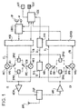
- This dual mode terminal illustrated in a simplified way by the figure, includes in particular a CLV keyboard and a display AFF, associated with a CDE control device, which allow the terminal user to control the terminal to access one of two radio systems at least, for example to the well-known GSM and DECT systems, and which allow it to exchange signals with these systems, for obtaining radio communications.
- These communications can take various forms. We have shown only an HP speaker and an M microphone for voice communications associated with a CODEC speech coder / decoder which is itself coupled to a MOD modulator and a DEMOD demodulator.
- the CE emission chain of this terminal also includes the MOD modulator, having two EI and EQ outputs on which are supplied baseband signals to transmit, two broadcast mixers MEI and MEQ whose outputs are jointly coupled to an amplifier AEM emission, the output of the latter, reaching, by a DUP duplexer ANT antenna.
- the reception chain CR of this terminal includes, at from the ANT antenna and the DUP duplexer, a ARC reception amplifier, two reception mixers MRI and MRQ providing RI and RQ inputs to the DEMOD demodulator for band reception signals based.
- the voice signals from the microphone M, coded in digital form in the CODEC coder / decoder are set in transmission format in the MOD modulator which produces signals to be transmitted in the form of transmission symbols successive each comprising two unit transmission signals respectively provided on the EI and EQ outputs.
- the unit emission signal EI affects the amplitude of a local phase emission wave 0 °.
- the signal unit EQ emission affects the amplitude of a local wave emission in phase quadrature with the previous one.
- the addition of these two local emission waves as well modulated, at the input of the emission amplifier AEM provides the radio signal to be transmitted or the transmission signal.
- a radio signal to receive, or signal reception, after amplification in the ARC amplifier identically attacks the reception mixers MRI and MRQ.
- the signal reception combines with a local phase reception wave 0 ° and this provides a unitary signal reception on the input RI of the DEMOD demodulator.
- the reception signal combines with a local wave reception in quadrature phase with the previous and this provides a unit reception signal on the RQ input of the DEMOD demodulator.
- the DEMOD demodulator recognize the symbols formed by these unit signals, demodulates them and provides coded speech signals to the CODEC encoder / decoder, which produces sounds through the speaker HP.
- the CDE control device is coupled, in particular, to the CODEC coder / decoder to take knowledge of the signals received and to control their operation.
- the terminal under the control of the user, by the means the AFF display and the CLV keyboard, acting on the CDE control device, or generated internal states periodically and automatically in the CDE command is at certain times in the state transmission to the DECT radio system.
- IEC, CEQ, CRI, CRQ switches, controlled by the CDE control device by links not shown, are in the positions shown in the Fig.
- the CDE control device is in relationship with a tunable source SYN, a synthesizer digital frequency, for example, and commands it to produce a local emission wave from the DECT system.
- This local wave is provided on the OL output of the SYN synthesizer and supplies a DECT transmission phase shifter DPH1, which provides to the first MEI emission mixer, by a first IEC emission switch in the position shown, a local wave DECT transmission of phase 0 ° and, on the second emission mixer MEQ, by a second emission switch CEQ in the position shown, a local emission wave DECT in phase quadrature.
- DECT transmission phase shifter DPH1 which provides to the first MEI emission mixer, by a first IEC emission switch in the position shown, a local wave DECT transmission of phase 0 ° and, on the second emission mixer MEQ, by a second emission switch CEQ in the position shown, a local emission wave DECT in phase quadrature.
- Signals to transmit thus modulate a local wave DECT emission supplied directly from the SYN tunable source.
- Some orders different from the CDE control device similarly allow to modulate other local waves DECT emission corresponding to other channels in the frequency band allocated to the DECT system. This
- the terminal does not receive. More generally, as long as the terminal does not receive not, the reception chain is blocked. It was illustrated, by way of example of a locking means, by the fact that CRI and CRQ receive switches are in the represented position, designated by RPR, in which the two receiving mixers MRI and MRQ receive no local wave.
- the terminal does not transmit.
- the broadcast chain is then blocked. This was illustrated, likewise, by the fact that the IEC and CEQ transmit switches are in a additional position, designated by RPE, in which the two emission mixers MEI and MEQ receive no waves local.
- the reception switches CRI and CRD are set by the CDE control device in such a position that they couple the MRI and MRQ receiving mixers to a DECT reception phase shifter DPH3, which receives a local wave DECT reception generated in the SYN synthesizer under the control of the CDE control device and product, to the first MRI receiving mixer, via the first switch CRI reception, a local DECT reception phase shifted by 0 ° and, towards the second MRQ receiving mixer, by the second CRQ receive switch, a local wave DECT reception in phase quadrature.
- the mixers reception MRI and MRQ can thus produce the signals RI and RQ baseband reception units towards the DEMOD demodulator.
- the latter coupled by a link of control with the CDE control device, provides coded signals to the CODEC coder / decoder which transforms them into voice signals from the loudspeaker.
- the same dual mode terminal shown in the figure is also intended for communications by another system radio communications such as the GSM system.
- radio communications such as the GSM system.
- the coding and formatting are suitable for this different system in MOD modulator, DEMOD demodulator, CODEC coder / decoder, different local waves must be provided for transmit and receive radio signals from this other system.
- the illustrated terminal comprises, downstream of said tunable source SYN, a frequency changer switchable DIV so that the source can respond directly to the needs of a radiocommunication system, as we have just seen, the insertion of said changer frequency, makes it capable of meeting the needs of a other radiocommunication system, thanks to a change determined from the frequency produced by said source SYN tunable provided by said DIV frequency changer.
- this frequency changer brings a division of the frequency provided by the SYN synthesizer by a determined factor, here equal to 2. It it is therefore a simple frequency division stage, such a flip-flop D, which is connected to the output dy SYN synthesizer and whose OL 'output provides the local wave GSM required.
- the GSM system uses the bands of frequencies 890 - 915 MHz and 935 - 960 MHz, i.e. overall 890 - 960 MHz.
- the invention provides for producing, using the source unique tunable which is the SYN synthesizer, frequencies in the band 1780 - 1920 MHz, to divide them by 2 using the DIV divider and thus obtain the frequencies required in the frequency band 890 - 960 MHz. More generally the invention plans to produce in the SYN synthesizer of frequencies in a matching band substantially to that directly provided by this synthesizer and change these frequencies by an operation such as the division, multiplication, addition or subtraction (there are simple circuits accomplishing these four operations) to obtain the frequencies of another band of frequency, or several other frequency bands, in a multimode terminal. Switching means, here CEI, CEQ, CRI, CRQ, allow you to choose between the different frequency bands.
- the terminal is put into GSM transmission by the CDE control device which places the two emission switch CEI and CEQ in a position such that the output OL 'of the divider DIV connected to a GSM DPH2 transmission phase shifter provides a local wave GSM transmission of phase 0 ° to the first mixer mixing MEI, and a local GSM transmission wave in quadrature phase at second emission mixer MEQ.
- the broadcast thus takes place, as described above, but in the GSM system. he it suffices that the SYN synthesizer, under the control of the CDE control device provides on its output Ol a twice the frequency of the GSM channel desired.
- a reception phase shifter GSM DPH4 receiving a local wave OL 'from the divider DIV, connected to the MRI and MRQ reception mixers by CRI and CRQ switches, allows reception of GSM signals.
Landscapes
- Engineering & Computer Science (AREA)
- Computer Networks & Wireless Communication (AREA)
- Signal Processing (AREA)
- Power Engineering (AREA)
- Transceivers (AREA)
- Input Circuits Of Receivers And Coupling Of Receivers And Audio Equipment (AREA)
- Connector Housings Or Holding Contact Members (AREA)
- Coupling Device And Connection With Printed Circuit (AREA)
- Switch Cases, Indication, And Locking (AREA)
- Superheterodyne Receivers (AREA)
- Circuits Of Receivers In General (AREA)
Claims (5)
- Funkkommunikationsendgerät, das eine einzige abstimmbare Quelle für lokale Sende- und/oder Empfangswellen, gebildet durch einen Frequenzsynthesizer, umfasst, um dem Endgerät das Senden und/oder Empfangen von Kanälen in verschiedenen, auf wenigstens zwei Funkkommunikationssysteme bezogenen Frequenzbändern zu ermöglichen, und dass Sende- bzw. Empfangsmischer (MRI, MRQ) umfasst, die mit einem Modulator (MOD) bzw. einem Demodulator (DEMOD) für Basisbandsignale verbunden sind, dadurch gekennzeichnet, dass das Endgerät hinter der abstimmbaren Quelle, die durch einen Frequenzsynthesizer (SYN) gebildet ist, der in der Lage ist, die Frequenzen eines von einem ersten System genutzten Bandes direkt zu liefern, einen Frequenzwandler (DIV) aufweist, der mit dem Synthesizer verbunden ist, um die Frequenzen, die dieser liefert, zu empfangen und sie auf Frequenzen eines anderen, von einem anderen System benutzten Bandes zu wandeln, und zwar durch eine Operation wie etwa eine Teilung, Multiplikation, Addition oder Subtraktion, sowie Schalter (CEI, CEQ, CRI, CRQ) umfasst, von denen jeder jeweils mit einem der Mischer verbunden ist, um an ihn eine lokale Welle, die von dem Synthesizer (SYN) oder von dem Wandler (DIV) kommt, unter der Wirkung einer Steuervorrichtung (CDE) zu übertragen, die es einem Benutzer ermöglicht, das Endgerät zu steuern, um alternativ auf das eine oder andere der Funkkommunikationssysteme zuzugreifen.
- Funkkommunikationsendgerät nach Anspruch 1, dadurch gekennzeichnet, dass der Frequenzwandler (DIV) eine Teilung der Frequenzen durch einen festgelegten Faktor vornimmt.
- Funkkommunikationsendgerät nach Anspruch 2, dadurch gekennzeichnet, dass der Faktor 2 ist.
- Funkkommunikationsendgerät nach Anspruch 1, 2 oder 3, dadurch gekennzeichnet, dass auf die Ausgänge des Synthesizers (SYN) und des Wandlers (DIV) jeweils ein Phasenschieber (DPH1 bis DPH4) folgt, der zwei um 90° phasenverschobene Wellen für die Modulation/Demodulation der Signale eines eine Quadraturmodulation anwendenden Funkkommunikationssystems liefert.
- Funkkommunikationsendgerät nach Anspruch 4, dadurch gekennzeichnet, dass nur zwei Mischer für die Modulation/Demodulation der Empfangssignale der zwei Funkkommunikationssysteme vorgesehen sind, wobei diese Mischer die um 90° phasenverschobenen Wellen von dem einen oder anderen der zwei Phasenschieber empfangen.
Applications Claiming Priority (2)
| Application Number | Priority Date | Filing Date | Title |
|---|---|---|---|
| FR9515396A FR2742946B1 (fr) | 1995-12-22 | 1995-12-22 | Terminal de radiocommunication multimode |
| FR9515396 | 1995-12-22 |
Publications (2)
| Publication Number | Publication Date |
|---|---|
| EP0780968A1 EP0780968A1 (de) | 1997-06-25 |
| EP0780968B1 true EP0780968B1 (de) | 2002-09-04 |
Family
ID=9485883
Family Applications (1)
| Application Number | Title | Priority Date | Filing Date |
|---|---|---|---|
| EP96402703A Expired - Lifetime EP0780968B1 (de) | 1995-12-22 | 1996-12-12 | Multimoden-Funkendgerät |
Country Status (5)
| Country | Link |
|---|---|
| US (1) | US5953641A (de) |
| EP (1) | EP0780968B1 (de) |
| AT (1) | ATE223629T1 (de) |
| DE (1) | DE69623426T2 (de) |
| FR (1) | FR2742946B1 (de) |
Families Citing this family (33)
| Publication number | Priority date | Publication date | Assignee | Title |
|---|---|---|---|---|
| JPH1141131A (ja) * | 1997-07-15 | 1999-02-12 | Toshiba Corp | 無線通信装置 |
| JP3825540B2 (ja) * | 1997-09-05 | 2006-09-27 | 松下電器産業株式会社 | 受信機および送受信機 |
| JP3848445B2 (ja) * | 1997-09-26 | 2006-11-22 | 松下電器産業株式会社 | 複数通信方式対応の無線機 |
| US6510310B1 (en) * | 1998-01-26 | 2003-01-21 | Conexant Systems, Inc. | Dual mode phone architecture utilizing a single transmit-receive switch |
| US7221921B2 (en) | 1998-05-29 | 2007-05-22 | Silicon Laboratories | Partitioning of radio-frequency apparatus |
| US6993314B2 (en) * | 1998-05-29 | 2006-01-31 | Silicon Laboratories Inc. | Apparatus for generating multiple radio frequencies in communication circuitry and associated methods |
| US7242912B2 (en) | 1998-05-29 | 2007-07-10 | Silicon Laboratories Inc. | Partitioning of radio-frequency apparatus |
| US7092675B2 (en) | 1998-05-29 | 2006-08-15 | Silicon Laboratories | Apparatus and methods for generating radio frequencies in communication circuitry using multiple control signals |
| US7035607B2 (en) | 1998-05-29 | 2006-04-25 | Silicon Laboratories Inc. | Systems and methods for providing an adjustable reference signal to RF circuitry |
| US20030003887A1 (en) * | 1998-05-29 | 2003-01-02 | Lysander Lim | Radio-frequency communication apparatus and associated methods |
| FI112741B (fi) * | 1998-11-26 | 2003-12-31 | Nokia Corp | Menetelmä ja järjestely RF-signaalien lähettämiseksi ja vastaanottamiseksi tiedonsiirtojärjestelmien erilaisissa radiorajapinnoissa |
| JP3326133B2 (ja) * | 1999-04-02 | 2002-09-17 | 松下電器産業株式会社 | 無線装置及び方法 |
| DE19916574C1 (de) * | 1999-04-13 | 2001-01-18 | Siemens Ag | Frequenzaufbereitungssystem für einen Mobilfunk-Dual Band-Sender/Empfänger (Transceiver) |
| US6826388B1 (en) * | 1999-11-15 | 2004-11-30 | Renesas Technology Corp. | Mobile communication apparatus including dividers in transmitter and receiver |
| DE19956073C2 (de) * | 1999-11-22 | 2002-03-28 | Infineon Technologies Ag | Modulationsanordnung |
| US6717981B1 (en) * | 1999-12-14 | 2004-04-06 | Koninklijke Philips Electronics N.V. | Transmitter image suppression in TDD transceivers |
| JP2001177433A (ja) * | 1999-12-21 | 2001-06-29 | Murata Mfg Co Ltd | 高周波複合部品及び移動体通信装置 |
| DE69921495T2 (de) * | 1999-12-23 | 2005-02-24 | Freescale Semiconductor, Inc., Austin | Doppelmodus mit einem einzelnen Empfängerschaltkreis |
| AU2001271082A1 (en) * | 2000-07-24 | 2002-02-05 | Matsushita Electric Industrial Co., Ltd. | Radio communication apparatus and radio communication method |
| US6665284B1 (en) * | 2000-07-31 | 2003-12-16 | Nokia Mobile Phones, Ltd. | Apparatus, and associated method, for receiving data at a radio device |
| US20020127985A1 (en) * | 2001-03-08 | 2002-09-12 | Fransis Bert L. | Wideband local oscillator architecture |
| US20020127992A1 (en) * | 2001-03-08 | 2002-09-12 | Fransis Bert L. | Wideband local oscillator architecture |
| DE10114779A1 (de) * | 2001-03-26 | 2002-10-24 | Infineon Technologies Ag | Sende-und Empfangseinheit |
| US6487398B1 (en) | 2001-08-14 | 2002-11-26 | Motorola, Inc. | Low noise architecture for a direct conversion transmitter |
| US20030092419A1 (en) * | 2001-11-09 | 2003-05-15 | Dan Nobbe | Method and apparatus for a near-unity divider in a direct conversion communication device |
| DE10317598A1 (de) * | 2003-04-16 | 2004-11-25 | Infineon Technologies Ag | Integrierter Transceiverschaltkreis |
| DE10345972B4 (de) * | 2003-10-02 | 2006-04-20 | Siemens Ag | Vorrichtung mit adaptiver Funksende- und/oder Funkempfangsarchitektur und Verfahren zu deren Betreiben |
| CN1625065A (zh) * | 2003-12-05 | 2005-06-08 | 皇家飞利浦电子股份有限公司 | 一种用于无线通信系统的接收机 |
| US20070173286A1 (en) * | 2005-04-04 | 2007-07-26 | Broadcom Corporation, A California Corporation | Distribution of shared local oscillation to multiple RF intefaces of a wireless device |
| US7912428B2 (en) * | 2005-11-16 | 2011-03-22 | Broadcom Corporation | System and method providing variable-frequency IF conversion in a multimode communication device |
| US7647026B2 (en) * | 2006-02-16 | 2010-01-12 | Broadcom Corporation | Receiver architecture for wireless transceiver |
| US7683851B2 (en) * | 2007-03-19 | 2010-03-23 | Broadcom Corporation | Method and system for using a single transformer for FM transmit and FM receive functions |
| JP4435257B1 (ja) * | 2008-12-24 | 2010-03-17 | 株式会社東芝 | 情報処理装置 |
Family Cites Families (9)
| Publication number | Priority date | Publication date | Assignee | Title |
|---|---|---|---|---|
| JPS584497B2 (ja) * | 1978-02-01 | 1983-01-26 | 株式会社ケンウッド | 局部発振装置 |
| US4969210A (en) * | 1988-02-10 | 1990-11-06 | Motorola, Inc. | Two-way radio having a PLL |
| JP2850160B2 (ja) * | 1991-01-25 | 1999-01-27 | 松下電器産業株式会社 | 時分割複信無線送受信装置 |
| GB9115350D0 (en) * | 1991-07-16 | 1991-08-28 | Navstar Ltd | A radio receiver |
| FI91819C (fi) * | 1991-11-05 | 1994-08-10 | Nokia Mobile Phones Ltd | Menetelmä kahden eri taajuusalueella toimivan digitaalisen radiopuhelimen taajuuksien muodostamiseksi |
| FR2707063B1 (de) * | 1993-06-25 | 1995-09-22 | Alcatel Mobile Comm France | |
| US5535432A (en) * | 1994-09-14 | 1996-07-09 | Ericsson Ge Mobile Communications Inc. | Dual-mode satellite/cellular phone with a frequency synthesizer |
| JPH08223071A (ja) * | 1995-02-08 | 1996-08-30 | Sony Corp | 送信機及び送受信機 |
| US5732330A (en) * | 1996-07-02 | 1998-03-24 | Ericsson Inc. | Dual band transceiver |
-
1995
- 1995-12-22 FR FR9515396A patent/FR2742946B1/fr not_active Expired - Fee Related
-
1996
- 1996-12-12 EP EP96402703A patent/EP0780968B1/de not_active Expired - Lifetime
- 1996-12-12 AT AT96402703T patent/ATE223629T1/de not_active IP Right Cessation
- 1996-12-12 DE DE69623426T patent/DE69623426T2/de not_active Expired - Fee Related
- 1996-12-20 US US08/777,733 patent/US5953641A/en not_active Expired - Fee Related
Also Published As
| Publication number | Publication date |
|---|---|
| FR2742946B1 (fr) | 1998-01-16 |
| EP0780968A1 (de) | 1997-06-25 |
| DE69623426D1 (de) | 2002-10-10 |
| DE69623426T2 (de) | 2003-04-30 |
| FR2742946A1 (fr) | 1997-06-27 |
| US5953641A (en) | 1999-09-14 |
| ATE223629T1 (de) | 2002-09-15 |
Similar Documents
| Publication | Publication Date | Title |
|---|---|---|
| EP0780968B1 (de) | Multimoden-Funkendgerät | |
| EP0631400B1 (de) | Tragbare Sende-Empfängeranordnung für digitale Signale mit 2 Betriebsarten | |
| JP4582752B2 (ja) | 時分割デュプレックストランシーバ中の送信器イメージの抑制 | |
| CA2016630C (en) | System for interrupting a transmitter output wave | |
| US6847812B2 (en) | Frequency-stabilized transceiver configuration | |
| KR20050029237A (ko) | 무선 송수신기 아키텍쳐 및 방법 | |
| GB2349309A (en) | Transceiver with bidirectional internal interface lines | |
| FR2755556A1 (fr) | Modulateur de frequence, emetteur et emetteur-recepteur incorporant ce modulateur de frequence | |
| GB2365638A (en) | Radio set and frequency converting method therefor | |
| EP0878916A3 (de) | Zweibanddatenkommunikationsgerät | |
| US5319675A (en) | Quadrature modulation circuit | |
| US4633511A (en) | Signal transmission and reception system | |
| US6973136B2 (en) | Radio communications apparatus | |
| JPH1141302A (ja) | 多変調フレーム発信機/受信機 | |
| GB2261345A (en) | Transceiver having a feedback loop | |
| US7409008B2 (en) | Transmitting arrangement for mobile radio | |
| FR2795280A1 (fr) | Telephone mobile comportant un dispositif d'emission d'un signal module en phase et en amplitude et son procede associe | |
| JP2004538709A (ja) | デジタル送信用の低減された周波数源を有するマルチバンドトランシーバ | |
| KR20020000895A (ko) | 통신 시스템 | |
| FR2822000A1 (fr) | Dispositif d'emission limitant les parasites hors de la bande de frequence allouee | |
| HUT73702A (en) | A communication device for computer networks, particularly of the cordless type | |
| JP3399135B2 (ja) | 高周波デジタル信号受信装置 | |
| AU6578600A (en) | Modulating method and device in a transmitter | |
| JP2003018231A (ja) | デジタル変調送信機 | |
| EP0555132A1 (de) | Breitbandiger Überlagerungsempfänger |
Legal Events
| Date | Code | Title | Description |
|---|---|---|---|
| PUAI | Public reference made under article 153(3) epc to a published international application that has entered the european phase |
Free format text: ORIGINAL CODE: 0009012 |
|
| AK | Designated contracting states |
Kind code of ref document: A1 Designated state(s): AT BE CH DE DK ES FI GB IT LI NL SE |
|
| 17P | Request for examination filed |
Effective date: 19971229 |
|
| 17Q | First examination report despatched |
Effective date: 20000306 |
|
| GRAG | Despatch of communication of intention to grant |
Free format text: ORIGINAL CODE: EPIDOS AGRA |
|
| GRAG | Despatch of communication of intention to grant |
Free format text: ORIGINAL CODE: EPIDOS AGRA |
|
| GRAH | Despatch of communication of intention to grant a patent |
Free format text: ORIGINAL CODE: EPIDOS IGRA |
|
| GRAH | Despatch of communication of intention to grant a patent |
Free format text: ORIGINAL CODE: EPIDOS IGRA |
|
| GRAA | (expected) grant |
Free format text: ORIGINAL CODE: 0009210 |
|
| RAP1 | Party data changed (applicant data changed or rights of an application transferred) |
Owner name: ALCATEL |
|
| AK | Designated contracting states |
Kind code of ref document: B1 Designated state(s): AT BE CH DE DK ES FI GB IT LI NL SE |
|
| PG25 | Lapsed in a contracting state [announced via postgrant information from national office to epo] |
Ref country code: NL Free format text: LAPSE BECAUSE OF FAILURE TO SUBMIT A TRANSLATION OF THE DESCRIPTION OR TO PAY THE FEE WITHIN THE PRESCRIBED TIME-LIMIT Effective date: 20020904 Ref country code: FI Free format text: LAPSE BECAUSE OF FAILURE TO SUBMIT A TRANSLATION OF THE DESCRIPTION OR TO PAY THE FEE WITHIN THE PRESCRIBED TIME-LIMIT Effective date: 20020904 Ref country code: AT Free format text: LAPSE BECAUSE OF FAILURE TO SUBMIT A TRANSLATION OF THE DESCRIPTION OR TO PAY THE FEE WITHIN THE PRESCRIBED TIME-LIMIT Effective date: 20020904 |
|
| REF | Corresponds to: |
Ref document number: 223629 Country of ref document: AT Date of ref document: 20020915 Kind code of ref document: T |
|
| REG | Reference to a national code |
Ref country code: GB Ref legal event code: FG4D Free format text: NOT ENGLISH |
|
| REG | Reference to a national code |
Ref country code: CH Ref legal event code: EP |
|
| GBT | Gb: translation of ep patent filed (gb section 77(6)(a)/1977) |
Effective date: 20020904 |
|
| REF | Corresponds to: |
Ref document number: 69623426 Country of ref document: DE Date of ref document: 20021010 |
|
| PG25 | Lapsed in a contracting state [announced via postgrant information from national office to epo] |
Ref country code: SE Free format text: LAPSE BECAUSE OF FAILURE TO SUBMIT A TRANSLATION OF THE DESCRIPTION OR TO PAY THE FEE WITHIN THE PRESCRIBED TIME-LIMIT Effective date: 20021204 Ref country code: DK Free format text: LAPSE BECAUSE OF FAILURE TO SUBMIT A TRANSLATION OF THE DESCRIPTION OR TO PAY THE FEE WITHIN THE PRESCRIBED TIME-LIMIT Effective date: 20021204 |
|
| PG25 | Lapsed in a contracting state [announced via postgrant information from national office to epo] |
Ref country code: LI Free format text: LAPSE BECAUSE OF NON-PAYMENT OF DUE FEES Effective date: 20021231 Ref country code: CH Free format text: LAPSE BECAUSE OF NON-PAYMENT OF DUE FEES Effective date: 20021231 Ref country code: BE Free format text: LAPSE BECAUSE OF NON-PAYMENT OF DUE FEES Effective date: 20021231 |
|
| NLV1 | Nl: lapsed or annulled due to failure to fulfill the requirements of art. 29p and 29m of the patents act | ||
| PG25 | Lapsed in a contracting state [announced via postgrant information from national office to epo] |
Ref country code: ES Free format text: LAPSE BECAUSE OF FAILURE TO SUBMIT A TRANSLATION OF THE DESCRIPTION OR TO PAY THE FEE WITHIN THE PRESCRIBED TIME-LIMIT Effective date: 20030328 |
|
| BERE | Be: lapsed |
Owner name: *ALCATEL Effective date: 20021231 |
|
| PLBE | No opposition filed within time limit |
Free format text: ORIGINAL CODE: 0009261 |
|
| STAA | Information on the status of an ep patent application or granted ep patent |
Free format text: STATUS: NO OPPOSITION FILED WITHIN TIME LIMIT |
|
| REG | Reference to a national code |
Ref country code: CH Ref legal event code: PL |
|
| 26N | No opposition filed |
Effective date: 20030605 |
|
| PGFP | Annual fee paid to national office [announced via postgrant information from national office to epo] |
Ref country code: IT Payment date: 20071221 Year of fee payment: 12 |
|
| PGFP | Annual fee paid to national office [announced via postgrant information from national office to epo] |
Ref country code: GB Payment date: 20071218 Year of fee payment: 12 |
|
| PGFP | Annual fee paid to national office [announced via postgrant information from national office to epo] |
Ref country code: DE Payment date: 20071221 Year of fee payment: 12 |
|
| GBPC | Gb: european patent ceased through non-payment of renewal fee |
Effective date: 20081212 |
|
| PG25 | Lapsed in a contracting state [announced via postgrant information from national office to epo] |
Ref country code: DE Free format text: LAPSE BECAUSE OF NON-PAYMENT OF DUE FEES Effective date: 20090701 |
|
| PG25 | Lapsed in a contracting state [announced via postgrant information from national office to epo] |
Ref country code: GB Free format text: LAPSE BECAUSE OF NON-PAYMENT OF DUE FEES Effective date: 20081212 |
|
| PG25 | Lapsed in a contracting state [announced via postgrant information from national office to epo] |
Ref country code: IT Free format text: LAPSE BECAUSE OF NON-PAYMENT OF DUE FEES Effective date: 20081212 |