EP0780977A1 - Präzises digitales Phasenschieberelement - Google Patents
Präzises digitales Phasenschieberelement Download PDFInfo
- Publication number
- EP0780977A1 EP0780977A1 EP96120406A EP96120406A EP0780977A1 EP 0780977 A1 EP0780977 A1 EP 0780977A1 EP 96120406 A EP96120406 A EP 96120406A EP 96120406 A EP96120406 A EP 96120406A EP 0780977 A1 EP0780977 A1 EP 0780977A1
- Authority
- EP
- European Patent Office
- Prior art keywords
- signal
- phase shift
- phase
- output
- frequency
- Prior art date
- Legal status (The legal status is an assumption and is not a legal conclusion. Google has not performed a legal analysis and makes no representation as to the accuracy of the status listed.)
- Granted
Links
- 230000010363 phase shift Effects 0.000 title claims abstract description 66
- 230000009977 dual effect Effects 0.000 claims abstract description 20
- 230000000737 periodic effect Effects 0.000 claims description 4
- 230000000644 propagated effect Effects 0.000 claims description 3
- 230000001902 propagating effect Effects 0.000 claims description 2
- 238000012217 deletion Methods 0.000 abstract description 9
- 230000037430 deletion Effects 0.000 abstract description 9
- 238000010586 diagram Methods 0.000 description 11
- 238000013459 approach Methods 0.000 description 8
- 230000008859 change Effects 0.000 description 7
- 230000000694 effects Effects 0.000 description 5
- 238000013461 design Methods 0.000 description 4
- 238000000034 method Methods 0.000 description 3
- 230000008569 process Effects 0.000 description 3
- 230000006872 improvement Effects 0.000 description 2
- 230000009471 action Effects 0.000 description 1
- 230000015572 biosynthetic process Effects 0.000 description 1
- 230000003247 decreasing effect Effects 0.000 description 1
- 230000003111 delayed effect Effects 0.000 description 1
- 230000001419 dependent effect Effects 0.000 description 1
- 238000011161 development Methods 0.000 description 1
- 238000004519 manufacturing process Methods 0.000 description 1
- 230000007246 mechanism Effects 0.000 description 1
- 230000003071 parasitic effect Effects 0.000 description 1
- 238000003786 synthesis reaction Methods 0.000 description 1
Images


Classifications
-
- H—ELECTRICITY
- H03—ELECTRONIC CIRCUITRY
- H03H—IMPEDANCE NETWORKS, e.g. RESONANT CIRCUITS; RESONATORS
- H03H17/00—Networks using digital techniques
- H03H17/08—Networks for phase shifting
-
- H—ELECTRICITY
- H03—ELECTRONIC CIRCUITRY
- H03K—PULSE TECHNIQUE
- H03K5/00—Manipulating of pulses not covered by one of the other main groups of this subclass
- H03K5/13—Arrangements having a single output and transforming input signals into pulses delivered at desired time intervals
-
- G—PHYSICS
- G01—MEASURING; TESTING
- G01S—RADIO DIRECTION-FINDING; RADIO NAVIGATION; DETERMINING DISTANCE OR VELOCITY BY USE OF RADIO WAVES; LOCATING OR PRESENCE-DETECTING BY USE OF THE REFLECTION OR RERADIATION OF RADIO WAVES; ANALOGOUS ARRANGEMENTS USING OTHER WAVES
- G01S7/00—Details of systems according to groups G01S13/00, G01S15/00, G01S17/00
- G01S7/02—Details of systems according to groups G01S13/00, G01S15/00, G01S17/00 of systems according to group G01S13/00
- G01S7/28—Details of pulse systems
- G01S7/282—Transmitters
-
- G—PHYSICS
- G01—MEASURING; TESTING
- G01S—RADIO DIRECTION-FINDING; RADIO NAVIGATION; DETERMINING DISTANCE OR VELOCITY BY USE OF RADIO WAVES; LOCATING OR PRESENCE-DETECTING BY USE OF THE REFLECTION OR RERADIATION OF RADIO WAVES; ANALOGOUS ARRANGEMENTS USING OTHER WAVES
- G01S7/00—Details of systems according to groups G01S13/00, G01S15/00, G01S17/00
- G01S7/02—Details of systems according to groups G01S13/00, G01S15/00, G01S17/00 of systems according to group G01S13/00
- G01S7/28—Details of pulse systems
- G01S7/285—Receivers
Definitions
- This invention relates to the field of RF phase shifters, and more particularly to phase shifters employing digital circuitry to achieve precise phase shift control.
- VFO variable frequency oscillator
- phase tuning approach requires a precision phase shifter.
- the prior art for electrically tuned phase shifters is wide and diverse, including analog designs using varactor tuning, switched line lengths, tapped delay lines, vector modulators, n-stage reactively terminated quadrature hybrids, and direct digital synthesizers (DDS).
- DDS direct digital synthesizers
- the phase resolution and accuracy that can be achieved from these approaches is limited by fabrication precision, alignment, and parasitic effects.
- the DDS can achieve the phase resolution of the disclosed approach but, without specialized and complex added circuitry, does not provide the spurious signal performance required for radar application.
- a precision digital frequency divider and phase shift system for frequency dividing the frequency (Fclk) of a periodic pulse train and precisely setting the relative phase of the output signal in relation to the prior phase of the output signal.
- the system includes frequency division circuit means responsive to the periodic input pulse train to produce an output signal having a frequency equal to Fclk/N, where N is an integer, and phase shift control circuit means operatively connected to the frequency division circuit means for selecting the relative output phase of the output signal relative to the prior phase of the output signal to a phase shift magnitude equivalent to 360C/N degrees, where C is a phase shift control parameter.
- the frequency division circuit means in one exemplary embodiment includes a divide-by-N frequency divider circuit
- the phase shift control circuit means includes a gate circuit having an input port connected to receive the input pulse train and an output connected to an input port of the divide-by-N frequency divider circuit.
- the gate circuit comprising means responsive to a gate signal for selectively propagating said the input train signal to the input port of the frequency divider, wherein one or more pulses comprising the input pulse train are selectively not propagated to the input port to achieve a desired phase shift.
- the frequency divider circuit means includes a dual modulus frequency divider circuit for selectively dividing the frequency of the input pulse train by N or M, the frequency divider circuit having an input port, an output port, and a modulus control port.
- the input pulse train is received at the divider circuit input port.
- a divider control circuit generates the modulus control signal, and is responsive to a phase control signal indicative of a phase shift value, to a phase shift strobe signal to initiate the phase shift, and to the system output signal.
- the divider control circuit commands the dual modulus frequency divider circuit to divide the input pulse train signal frequency by N except during a phase shift time interval during which the frequency divider circuit is commanded to divide the input pulse train signal frequency by M to achieve the desired relative phase shift.
- the value of M can be equal to N+1, to a fixed integer or rational number, or can be a programmable value.
- a digital phase shifter is described that provides precise phase shifting of an input signal by increments of 360/N degrees, where N is an integer.
- the input to the phase shifter can be a pulse train, or another waveform that is converted to a square wave or pulse train prior to inputting to the phase shifter.
- the output is a pulse train at a frequency divided by N and has N equally spaced phase states.
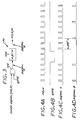
- a basic frequency divider element 50 with a clock signal input at Fclk frequency and an output at frequency Fclk/N is shown in FIG. 1.
- the output signal phase state from a free running frequency divider is not controlled and will depend on the initial state of the frequency divider.
- the frequency divider 50 is essentially a digital counter that counts input pulses and outputs a pulse every N input pulses. The phase state is therefore dependent on the initial count in the divider when the input pulse train is applied or when the frequency divider dc power is applied.
- FIG. 2A illustrates the signal waveform of the clock signal input to the frequency divider element 50 of FIG. 1.
- FIGS. 2B-2F illustrate the N possible output signal phase states that result from the frequency division process of the circuit of FIG. 1. This behavior of digital frequency dividers is well known.
- the invention addresses the means by which the relative phase state of the output signal of the frequency divider can be reliably controlled. Exemplary embodiments for this control are disclosed, and each relies on what is effectively selective deletion of pulses from the input signal pulse train.
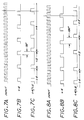
- FIG. 3 A direct approach to accomplish this pulse deletion is shown in schematic form in FIG. 3; the associated signal timing diagrams are shown in FIG. 4.
- An input clock signal is connected to one input of AND gate 102 comprising the phase shift system 100.
- the input clock signal is free running at a constant frequency, Fclk, as shown in the waveform illustrated in FIG. 4A.
- a gate signal (FIG. 4B) applied to the other input to the AND gate 102 determines when the clock signal is applied to the divide-by-N frequency divider 104.
- the gate signal is low (logic-0)
- the AND gate output is held to logic-0, and the clock signal is blocked from reaching the divider 104.
- the gate signal is logic-1, the input to the divider is identically the clock signal, as shown in FIG.
- FIG. 4C which represents the signal at A, the input to the divider 104.
- the frequency divider maintains its internal state (or count) during the time the divider input is interrupted by the gate signal.
- the divider 104 resumes counting, but the gating action has caused a delay in the generation of subsequent output pulses as shown in FIG. 4D, illustrating the signal at B, the output of the divide-by-N element 104.
- the frequency divider 104 is dividing by three and the gating spans two periods of the clock signal. For division by three, there are three possible output signal phase states spaced 120 degrees apart. The two clock signal period gating interval produces a 240 degree phase change to the output signal.
- Signals input to the phase shift element include the input signal that is the signal to be frequency divided and phase shifted, an n-bit phase control signal that determines the magnitude of the desired phase shift of the divider output, and a phase shift strobe signal that initiates the actual phase change.
- the input signal is passed through the AND gate 102 and clocks the divide-by-N frequency divider 104 to produce an output at 1/N th the input frequency.
- the input signal also serves as the input to n-bit counter 110.
- the n-bit phase control signal is set to the binary number that corresponds to the number of pulses of the input that are to be blocked from reaching the frequency divider 104.
- the n-bit phase control signal is provided at the parallel load port of the counter 110. If N is selected to be 16 in FIG. 5, the range of the phase control signal will be zero through fifteen resulting in the phase control signal being a 4-bit command word.
- the phase shift strobe is a short pulse signal that is applied to initiate the phase shifting process.
- the phase shift strobe activates the preset enable function of the n-bit counter 110 to load the phase control signal as a starting state in the counter. Simultaneously, the phase shift strobe resets the R/S flip-flop 106 to produce logic-0 at the Q output.
- the AND gate 102 then blocks the input signal from reaching the frequency divider 104. Subsequent pulses of the input signal inputted to the clock input of the n-bit counter 110 function to decimate the count by one for each input pulse. Thus, the initial value loaded in the counter 110 is progressively decreased by each input signal pulse until zero is reached.
- a second embodiment of pulse deletion to effect controllable phase shift in accordance with the invention is shown in FIG. 6.
- the system 120 employs a dual modulus frequency divider 122 as the primary phase shifting element.
- Such frequency dividers divide the input frequency by N or N+M, depending on the state of an input modulus control signal.
- N can be any integer but is typically in the range of 3 to 100.
- M is usually 1 or 2 but could be other integers as well as non-integer values.
- Dual modulus frequency dividers were originally designed for use with two additional programmable counters in frequency synthesis applications to provide programmable integer frequency division factors in unit steps over a wide range.
- a divider control circuit 124 provides a modulus control signal to the divider 122 to set the divider modulus.
- FIGS. 7A-7C show the basic mechanism for this phase adjustment.
- FIG. 7A shows the input signal, represented as a pulse train
- FIG. 7B shows that signal divided continuously by N (4 in this example).
- FIG. 7C shows a similar output except that, for one cycle of division, the dual modulus frequency divider is set to divide by N+1 (5 in this example) and then is reset to divide by N.
- the output signal is retarded by 1/N th of the period of the signal of FIG. 7B.
- FIGS. 8A-8C are similar to FIG. 7, but show the case with two cycles of division by N+1.
- the relative phase shift is seen to be 2 ⁇ (360/N), or 180 degrees in this example.
- each added cycle of division by N+1 will increment an additional 360/N degrees.
- C is the number of cycles of division by N+1
- the dual modulus frequency divider produces the same effect as the deletion of an input pulse for each cycle of frequency division by N+1.
- each cycle of division by N+1 has delayed the output pulse by one period of the input pulse frequency as shown in FIGS. 7 and 8.
- the divider control 124 comprises an R/S flip-flop 126, an AND gate 128 and an n-bit digital counter 130, which operate in a similar manner to corresponding elements of the circuit implementation shown in FIG. 5, except that the clock to the counter 130 is taken from the output of divider 122 instead of from the input to the divider.
- the n-bit phase control signal is applied to the parallel load port of the counter 130. This phase control signal determines the number of cycles that the dual modulus frequency divider 122 will divide by N+1.
- the phase shift strobe is applied to the preset enable port of the counter 130, to initiate the phase change, and is a pulse signal that functions to load the phase control signal into the n-bit digital counter as an initial value.
- the phase shift strobe also resets the R/S flip-flop to produce a logic-0 output to the ⁇ N/ ⁇ (N+1), dual modulus frequency divider, setting it to divide by N+1. Subsequently, each output pulse from the ⁇ N/ ⁇ (N+1) frequency divider 122 reduces the count value of the digital counter 130 by one. When the digital counter reaches a value of zero, the n complemented Q-bar outputs from the counter 130 will all be logic-1.
- That input to the n-input AND gate 128 will cause the set input to the R/S flip-flop 126 to be switched to logic-1, setting the R/S flip-flop output to logic-1.
- the logic-1 input to the ⁇ N/ ⁇ (N+1) frequency divider will cause the frequency division factor to return to division by N.
- the ⁇ N/ ⁇ (N+1) frequency divider will divide the input signal frequency by N+1 for the number of cycles commanded by the phase control signal and then revert to division by N.
- a difference between the input pulse gating (FIG. 3) and dual modulus frequency division (FIG. 6) approaches is that the gating approach accomplishes all of the commanded phase shift in one gating (or output pulse) interval whereas the dual modulus frequency divider approach with division factors of N and N+1 accomplishes the phase shift progressively over C output pulse intervals.
- a third embodiment of the digital phase shifter is shown in FIG. 10 and is an extension of the configuration shown in FIG. 6 to allow the frequency divider modulus of dual modulus divider 122' to be N and N+M, where M may be any rational number (integer, fraction, or integer plus fraction).
- the minimum phase shift increment is 360 ⁇ M/N degrees.
- a fourth embodiment of the digital phase shifter is shown in FIG. 11 and is an extension of the configuration shown in FIG. 10 to allow M to be programmable.
- the divider 122'' receives two control signals from divider control circuit 124'', the modulus control signal to select which of two modulus are to be applied, and an M control signal to set the value for M.
- the minimum phase shift increment is 360/N degrees for M programmable in integer steps. Programming M over a range of 0 to N-1 will provide phase control over a 360 degree range in 360/N degree increments.
- FIG. 11 requires a more complex multiple modulus frequency divider than the configurations of FIG. 5 and FIG. 10, it provides a commanded phase change in one cycle of frequency division by N+M instead of up to N-1 cycles with the approach of FIG. 6.
- a precision digital phase shift circuit 100; 120 for achieving precise phase shift of an input pulse train signal.
- the output is a pulse train at a frequency equal to the input signal frequency divided by N, and having N equally spaced phase states.
- the relative phase state of the output signal is reliably controlled by selective deletion of pulses from the input signal pulse train.
- the selective deletion can be achieved by selectively gating 102 the input pulse train, or by use of a dual modulus frequency divider circuit 122.
Landscapes
- Physics & Mathematics (AREA)
- Nonlinear Science (AREA)
- Pulse Circuits (AREA)
- Manipulation Of Pulses (AREA)
- Radar Systems Or Details Thereof (AREA)
- Networks Using Active Elements (AREA)
- Stabilization Of Oscillater, Synchronisation, Frequency Synthesizers (AREA)
Applications Claiming Priority (2)
| Application Number | Priority Date | Filing Date | Title |
|---|---|---|---|
| US08/576,330 US5650738A (en) | 1995-12-21 | 1995-12-21 | Precision digital phase shift element |
| US576330 | 1995-12-21 |
Publications (2)
| Publication Number | Publication Date |
|---|---|
| EP0780977A1 true EP0780977A1 (de) | 1997-06-25 |
| EP0780977B1 EP0780977B1 (de) | 2000-08-09 |
Family
ID=24303983
Family Applications (1)
| Application Number | Title | Priority Date | Filing Date |
|---|---|---|---|
| EP96120406A Expired - Lifetime EP0780977B1 (de) | 1995-12-21 | 1996-12-18 | Präzises digitales Phasenschieberelement |
Country Status (6)
| Country | Link |
|---|---|
| US (1) | US5650738A (de) |
| EP (1) | EP0780977B1 (de) |
| JP (2) | JPH104333A (de) |
| DE (1) | DE69609698T2 (de) |
| ES (1) | ES2148666T3 (de) |
| IL (1) | IL119859A (de) |
Families Citing this family (4)
| Publication number | Priority date | Publication date | Assignee | Title |
|---|---|---|---|---|
| FR2782422B1 (fr) * | 1998-08-13 | 2000-09-15 | St Microelectronics Sa | Circuit de mesure d'intervalles de temps auto-calibre |
| US6049302A (en) * | 1999-05-04 | 2000-04-11 | Boeing North American | Pulsed doppler radar system with small intermediate frequency filters |
| US6459404B1 (en) | 2000-08-28 | 2002-10-01 | Raytheon Company | DDS spur mitigation in a high performance radar exciter |
| US7395286B1 (en) * | 2004-01-05 | 2008-07-01 | National Semiconductor Corporation | Method for generating non-overlapping N-phases of divide-by-N clocks with precise 1/N duty ratio using a shift register |
Citations (2)
| Publication number | Priority date | Publication date | Assignee | Title |
|---|---|---|---|---|
| EP0125811A2 (de) * | 1983-05-17 | 1984-11-21 | Marconi Instruments Limited | Frequenzgenerator |
| US4560960A (en) * | 1982-03-05 | 1985-12-24 | Thomson Csf | Digital frequency synthesizer for generating a frequency-modulated signal and radio frequency apparatus including such a device |
Family Cites Families (3)
| Publication number | Priority date | Publication date | Assignee | Title |
|---|---|---|---|---|
| NL7003278A (de) * | 1970-03-07 | 1971-09-09 | ||
| FR2600847B1 (fr) * | 1986-06-25 | 1988-10-21 | Sfim | Dispositif generateur de signaux a frequence variable programmable |
| US5020079A (en) * | 1989-11-17 | 1991-05-28 | Nynex Corporation | Apparatus for generating a minimum-shift-keying signal |
-
1995
- 1995-12-21 US US08/576,330 patent/US5650738A/en not_active Expired - Lifetime
-
1996
- 1996-12-18 IL IL11985996A patent/IL119859A/xx not_active IP Right Cessation
- 1996-12-18 EP EP96120406A patent/EP0780977B1/de not_active Expired - Lifetime
- 1996-12-18 DE DE69609698T patent/DE69609698T2/de not_active Expired - Lifetime
- 1996-12-18 ES ES96120406T patent/ES2148666T3/es not_active Expired - Lifetime
- 1996-12-20 JP JP8342175A patent/JPH104333A/ja active Pending
-
2000
- 2000-05-29 JP JP2000158788A patent/JP2001016071A/ja active Pending
Patent Citations (2)
| Publication number | Priority date | Publication date | Assignee | Title |
|---|---|---|---|---|
| US4560960A (en) * | 1982-03-05 | 1985-12-24 | Thomson Csf | Digital frequency synthesizer for generating a frequency-modulated signal and radio frequency apparatus including such a device |
| EP0125811A2 (de) * | 1983-05-17 | 1984-11-21 | Marconi Instruments Limited | Frequenzgenerator |
Non-Patent Citations (1)
| Title |
|---|
| PATERSON J D: "Digital phase shifters", MARCONI REVIEW, 1973, UK, vol. 36, no. 190, ISSN 0025-2883, pages 193 - 199, XP002027645 * |
Also Published As
| Publication number | Publication date |
|---|---|
| IL119859A0 (en) | 1997-03-18 |
| DE69609698D1 (de) | 2000-09-14 |
| JPH104333A (ja) | 1998-01-06 |
| DE69609698T2 (de) | 2001-03-29 |
| JP2001016071A (ja) | 2001-01-19 |
| EP0780977B1 (de) | 2000-08-09 |
| IL119859A (en) | 2001-03-19 |
| US5650738A (en) | 1997-07-22 |
| ES2148666T3 (es) | 2000-10-16 |
Similar Documents
| Publication | Publication Date | Title |
|---|---|---|
| US5268656A (en) | Programmable clock skew adjustment circuit | |
| US6061418A (en) | Variable clock divider with selectable duty cycle | |
| US4290022A (en) | Digitally programmable phase shifter | |
| US5261081A (en) | Sequence control apparatus for producing output signals in synchronous with a consistent delay from rising or falling edge of clock input signal | |
| JPH0548446A (ja) | 半導体集積回路 | |
| US4002995A (en) | Digital frequency synthesizer having selectable frequency offset between transmit and receive frequencies | |
| GB2055268A (en) | Digital phase comparator circuit | |
| GB991525A (en) | A digital frequency synthesis device | |
| US3714589A (en) | Digitally controlled phase shifter | |
| US5214682A (en) | High resolution digitally controlled oscillator | |
| EP0780977A1 (de) | Präzises digitales Phasenschieberelement | |
| US4560960A (en) | Digital frequency synthesizer for generating a frequency-modulated signal and radio frequency apparatus including such a device | |
| US6249188B1 (en) | Error-suppressing phase comparator | |
| US5036297A (en) | High-speed digital PLL device | |
| US5652534A (en) | Precision digital phase shifter | |
| US5335253A (en) | Non-integral frequency division using regulated digital divider circuits | |
| US4942595A (en) | Circuit for dividing the frequency of a digital clock signal by two and one-half | |
| US5703514A (en) | Digital frequency divider phase shifter | |
| US5323436A (en) | Apparatus of and method for counting a number of revolutions of a servo motor | |
| JPH1198007A (ja) | 分周回路 | |
| AU6570694A (en) | Numerically controlled oscillator and digital phase locked loop | |
| US5656958A (en) | Frequency synthesizing device | |
| CA1289251C (en) | Digital first order hold circuit | |
| US5987089A (en) | Programmable divider with controlled duty cycle | |
| SU1525880A1 (ru) | Устройство формировани сигналов |
Legal Events
| Date | Code | Title | Description |
|---|---|---|---|
| PUAI | Public reference made under article 153(3) epc to a published international application that has entered the european phase |
Free format text: ORIGINAL CODE: 0009012 |
|
| AK | Designated contracting states |
Kind code of ref document: A1 Designated state(s): DE ES GB |
|
| 17P | Request for examination filed |
Effective date: 19971202 |
|
| RAP1 | Party data changed (applicant data changed or rights of an application transferred) |
Owner name: RAYTHEON COMPANY |
|
| 17Q | First examination report despatched |
Effective date: 19990325 |
|
| GRAG | Despatch of communication of intention to grant |
Free format text: ORIGINAL CODE: EPIDOS AGRA |
|
| GRAG | Despatch of communication of intention to grant |
Free format text: ORIGINAL CODE: EPIDOS AGRA |
|
| GRAH | Despatch of communication of intention to grant a patent |
Free format text: ORIGINAL CODE: EPIDOS IGRA |
|
| GRAH | Despatch of communication of intention to grant a patent |
Free format text: ORIGINAL CODE: EPIDOS IGRA |
|
| GRAA | (expected) grant |
Free format text: ORIGINAL CODE: 0009210 |
|
| AK | Designated contracting states |
Kind code of ref document: B1 Designated state(s): DE ES GB |
|
| REF | Corresponds to: |
Ref document number: 69609698 Country of ref document: DE Date of ref document: 20000914 |
|
| REG | Reference to a national code |
Ref country code: ES Ref legal event code: FG2A Ref document number: 2148666 Country of ref document: ES Kind code of ref document: T3 |
|
| EN | Fr: translation not filed | ||
| PLBE | No opposition filed within time limit |
Free format text: ORIGINAL CODE: 0009261 |
|
| STAA | Information on the status of an ep patent application or granted ep patent |
Free format text: STATUS: NO OPPOSITION FILED WITHIN TIME LIMIT |
|
| 26N | No opposition filed | ||
| REG | Reference to a national code |
Ref country code: GB Ref legal event code: IF02 |
|
| PGFP | Annual fee paid to national office [announced via postgrant information from national office to epo] |
Ref country code: GB Payment date: 20151216 Year of fee payment: 20 Ref country code: DE Payment date: 20151215 Year of fee payment: 20 |
|
| PGFP | Annual fee paid to national office [announced via postgrant information from national office to epo] |
Ref country code: ES Payment date: 20151112 Year of fee payment: 20 |
|
| REG | Reference to a national code |
Ref country code: DE Ref legal event code: R071 Ref document number: 69609698 Country of ref document: DE |
|
| REG | Reference to a national code |
Ref country code: GB Ref legal event code: PE20 Expiry date: 20161217 |
|
| PG25 | Lapsed in a contracting state [announced via postgrant information from national office to epo] |
Ref country code: GB Free format text: LAPSE BECAUSE OF EXPIRATION OF PROTECTION Effective date: 20161217 |
|
| PG25 | Lapsed in a contracting state [announced via postgrant information from national office to epo] |
Ref country code: ES Free format text: LAPSE BECAUSE OF EXPIRATION OF PROTECTION Effective date: 20161219 |