EP0780984A1 - Circuit de sortie et dispositif electronique utilisant ledit circuit - Google Patents
Circuit de sortie et dispositif electronique utilisant ledit circuit Download PDFInfo
- Publication number
- EP0780984A1 EP0780984A1 EP96922222A EP96922222A EP0780984A1 EP 0780984 A1 EP0780984 A1 EP 0780984A1 EP 96922222 A EP96922222 A EP 96922222A EP 96922222 A EP96922222 A EP 96922222A EP 0780984 A1 EP0780984 A1 EP 0780984A1
- Authority
- EP
- European Patent Office
- Prior art keywords
- output
- potential
- output terminal
- transistor
- control
- Prior art date
- Legal status (The legal status is an assumption and is not a legal conclusion. Google has not performed a legal analysis and makes no representation as to the accuracy of the status listed.)
- Granted
Links
Images









Classifications
-
- H—ELECTRICITY
- H03—ELECTRONIC CIRCUITRY
- H03K—PULSE TECHNIQUE
- H03K19/00—Logic circuits, i.e. having at least two inputs acting on one output; Inverting circuits
- H03K19/0175—Coupling arrangements; Interface arrangements
- H03K19/0185—Coupling arrangements; Interface arrangements using field effect transistors only
-
- G—PHYSICS
- G11—INFORMATION STORAGE
- G11C—STATIC STORES
- G11C7/00—Arrangements for writing information into, or reading information out from, a digital store
- G11C7/10—Input/output [I/O] data interface arrangements, e.g. I/O data control circuits, I/O data buffers
- G11C7/1051—Data output circuits, e.g. read-out amplifiers, data output buffers, data output registers, data output level conversion circuits
- G11C7/1057—Data output buffers, e.g. comprising level conversion circuits, circuits for adapting load
-
- G—PHYSICS
- G11—INFORMATION STORAGE
- G11C—STATIC STORES
- G11C11/00—Digital stores characterised by the use of particular electric or magnetic storage elements; Storage elements therefor
- G11C11/21—Digital stores characterised by the use of particular electric or magnetic storage elements; Storage elements therefor using electric elements
- G11C11/34—Digital stores characterised by the use of particular electric or magnetic storage elements; Storage elements therefor using electric elements using semiconductor devices
- G11C11/40—Digital stores characterised by the use of particular electric or magnetic storage elements; Storage elements therefor using electric elements using semiconductor devices using transistors
- G11C11/41—Digital stores characterised by the use of particular electric or magnetic storage elements; Storage elements therefor using electric elements using semiconductor devices using transistors forming static cells with positive feedback, i.e. cells not needing refreshing or charge regeneration, e.g. bistable multivibrator or Schmitt trigger
-
- G—PHYSICS
- G11—INFORMATION STORAGE
- G11C—STATIC STORES
- G11C7/00—Arrangements for writing information into, or reading information out from, a digital store
- G11C7/10—Input/output [I/O] data interface arrangements, e.g. I/O data control circuits, I/O data buffers
- G11C7/1051—Data output circuits, e.g. read-out amplifiers, data output buffers, data output registers, data output level conversion circuits
-
- H—ELECTRICITY
- H03—ELECTRONIC CIRCUITRY
- H03K—PULSE TECHNIQUE
- H03K17/00—Electronic switching or gating, i.e. not by contact-making and –breaking
- H03K17/16—Modifications for eliminating interference voltages or currents
- H03K17/161—Modifications for eliminating interference voltages or currents in field-effect transistor switches
- H03K17/165—Modifications for eliminating interference voltages or currents in field-effect transistor switches by feedback from the output circuit to the control circuit
- H03K17/166—Soft switching
- H03K17/167—Soft switching using parallel switching arrangements
-
- H—ELECTRICITY
- H03—ELECTRONIC CIRCUITRY
- H03K—PULSE TECHNIQUE
- H03K19/00—Logic circuits, i.e. having at least two inputs acting on one output; Inverting circuits
- H03K19/003—Modifications for increasing the reliability for protection
- H03K19/00346—Modifications for eliminating interference or parasitic voltages or currents
- H03K19/00361—Modifications for eliminating interference or parasitic voltages or currents in field effect transistor circuits
-
- H—ELECTRICITY
- H03—ELECTRONIC CIRCUITRY
- H03K—PULSE TECHNIQUE
- H03K19/00—Logic circuits, i.e. having at least two inputs acting on one output; Inverting circuits
- H03K19/0175—Coupling arrangements; Interface arrangements
- H03K19/0185—Coupling arrangements; Interface arrangements using field effect transistors only
- H03K19/018507—Interface arrangements
- H03K19/018521—Interface arrangements of complementary type, e.g. CMOS
-
- H—ELECTRICITY
- H03—ELECTRONIC CIRCUITRY
- H03K—PULSE TECHNIQUE
- H03K19/00—Logic circuits, i.e. having at least two inputs acting on one output; Inverting circuits
- H03K19/02—Logic circuits, i.e. having at least two inputs acting on one output; Inverting circuits using specified components
- H03K19/08—Logic circuits, i.e. having at least two inputs acting on one output; Inverting circuits using specified components using semiconductor devices
- H03K19/094—Logic circuits, i.e. having at least two inputs acting on one output; Inverting circuits using specified components using semiconductor devices using field-effect transistors
- H03K19/0944—Logic circuits, i.e. having at least two inputs acting on one output; Inverting circuits using specified components using semiconductor devices using field-effect transistors using MOSFET or insulated gate field-effect transistors, i.e. IGFET
- H03K19/0948—Logic circuits, i.e. having at least two inputs acting on one output; Inverting circuits using specified components using semiconductor devices using field-effect transistors using MOSFET or insulated gate field-effect transistors, i.e. IGFET using CMOS or complementary insulated gate field-effect transistors
Definitions
- the present invention relates to an output circuit for a semiconductor device, and in particular to an output circuit providing high-speed data output and low noise characteristics, and also relates to an electronic apparatus using the same.
- presetting circuit As a means of solving these problems is known a circuit which preceding the data output sets the output lines to an intermediate potential, or the so-called intermediate potential setting circuit (referred to hereinafter as "presetting circuit").
- presetting circuit As examples of this type of circuit may be cited, for example, Japanese Patent Application Laid-Open No. 63-112893, Japanese Patent Application Laid-Open No. 63-117839, Japanese Patent Application Laid-Open No. 8-77775 (referred to hereinafter as "the first type"), and Japanese Patent Application Laid-Open No. 2-113493, Japanese Patent Application Laid-Open No. 1-149290 (referred to hereinafter as "the second type").
- Fig. 23A shows the structure of the first type as disclosed in Japanese Patent Application Laid-Open No. 63-112893 (referred to hereinafter as "prior art 1")
- Fig. 23B shows the structure of the first type as disclosed in Japanese Patent Application Laid-Open No. 63-112893
- Fig. 24A and 24B shows the case where the output capacitance C L is a low load capacitance, at approximately 30 pF
- Fig. 24B shows the case where the output capacitance C L is a high load capacitance, at 100 pF or more.
- an output terminal D out is set to an intermediate potential determined by the ability ratio of Nch transistor Q2a and Pch transistor Q1a. For example, if output terminal D out is initially high, the Pch transistor Q1a conducts, and the drain voltage DN rises, and consequently the potential of the output terminal D out falls as a result of the current I on2 and the current I on , thus being preset.
- an output circuit having output drive means including a first transistor which is connected to a power supply line and an output terminal and has a first control terminal to which is input a first control signal, and a second transistor which is connected to a ground line and the output terminal and has a second control terminal to which is input a second control signal, and based on the first and second control signals outputting a data signal from the output terminal;
- the shorting means may comprise switch means connected between the output terminal and the preset control terminal of the output preset transistor; and output potential detection means which detects the potential of the output terminal, and based on the detected output potential controls the switch means; and wherein before the data signal is output, the output potential detection means makes the switch means conducting according to the output terminal potential, and operates the output preset transistor to set the output terminal to a predetermined potential.
- the shorting means as a switch means and an output potential detection means, according as the output terminal is high or low, the at least one output preset transistor can be controlled, so that both rises and falls of the output terminal potential can be controlled freely. By this means, continuous through currents in the output preset transistors do not occur.
- the output preset transistor may comprise
- the third control terminal of the first preset transistor and the output terminal can be shorted by the first switch means.
- the fourth control terminal of the second preset transistor and the output terminal can be shorted by the second switch means.
- bi-directional presetting that is presetting when the output changes from low to high, and presetting when the output changes from high to low, can be achieved, short access times can be achieved, and this is effective for a device driven by a low voltage.
- an output circuit which comprises output drive means including a first transistor which is connected to a power supply line and an output terminal and has a first control terminal to which is input a first control signal, and a second transistor which is connected to a ground line and the output terminal and has a second control terminal to which is input a second control signal, and based on the first and second control signals outputting a data signal from the output terminal;
- the shorting means of a switch means and an output potential detection means By configuring the shorting means of a switch means and an output potential detection means, according as the output terminal is high or low, the at least one of the first and second transistors is controlled, so the both rises and falls of the output terminal potential can be controlled freely.
- the output control means controls the on/off operation of the first and second transistors by the output control means, for example in the case that the output terminal is low, the output terminal potential can be raised to a predetermined potential, and the first transistor can be turned off.
- the switch means is put in the off state, and then the first transistor is turned on, the rise from the predetermined potential to the power supply potential can be easily achieved.
- the output terminal potential can be lowered to a predetermined potential, and the second transistor can be turned off.
- the switch means is put in the off state, and then the second transistor is turned on, the fall from the predetermined potential to the ground potential can be easily achieved.
- an optimum device can be obtained.
- the setting means may comprise output control means which outputs the first and second control signals to the first and second control terminals of the first and second transistors to control the first and second transistors; and second switch means connected between the output control means and at least one of the first and second control terminals, and controlled by the output potential detection means.
- the output potential detection means makes the second switch means which is connected to one of the first and second control terminals non-conducting. In a state of preventing output of the data signal, the output control means operates one of the first and second transistors to set the output terminal to a predetermined potential intermediate between the power supply line potential and the ground line potential.
- the second switch means may be a transmission gate which sets the output control means and at least one of the first and second control terminals to be selectively one of conducting and non-conducting in accordance with a detected potential by the output potential detection means.
- the circuit configuration can be simplified.
- the second switch means may be formed of a first conductivity type transistor and a second conductivity type transistor.
- the output control means comprises:
- the circuit configuration can be made even simpler.
- the first switch means may comprise a first switch connected between the output terminal and the first control terminal of the first transistor, and a second switch connected between the output terminal and the second control terminal of the second transistor.
- the second switch means may comprise a third switch connected between the first control terminal of the first transistor and the output control means, and a fourth switch connected between the second control terminal of the second transistor and the output control means.
- the output potential detection means makes one of the first and second switch means conducting.
- the output control means operates one of the first and second transistors to set the output terminal to a predetermined potential intermediate between the power supply line potential and the ground line potential.
- bi-directional presetting that is presetting when the output changes from low to high, and presetting when the output changes from high to low, can be achieved, short access times can be achieved, and this is effective for a device driven by a low voltage.
- each of the first transistor and the second switch may be formed by a transistor of a first conductivity type
- each of the second transistor and the first switch may be formed by a transistor of a second conductivity type
- each of the third switch and the fourth switch may be formed by a transistor of the first conductivity type and a transistor of the second conductivity type.
- the first and second transistors of the output drive means and the switch shorting the output terminal are formed of a transistor of a first conductivity type or a second conductivity type, whereby the number of signal lines can be reduced, and the circuit scale and layout scale can be simplified, and the device can be made smaller.
- each of the first transistor, the second switch, and the third switch may be formed by a transistor of a first conductivity type
- each of the second transistor, the first switch, and the fourth switch may be formed by a transistor of a second conductivity type.
- all of the switches can be formed by a single transistor, and the circuit scale and layout area can be even further reduced, and the device can be made even yet smaller.
- a semiconductor device with a large number of output terminals such as, for example, an 8-bit, 16-bit, or 32-bit or similar device, a smaller chip size can be achieved.
- an output circuit for outputting a data signal after setting an output terminal to a potential intermediate between a power supply line potential and a ground line potential comprising:
- the output terminal potential in the case that the output terminal potential is lowered, and in the case that the output terminal potential is high, firstly the potential of the output terminal is lowered to the intermediate potential by the potential setting means. At this time, close to the threshold value of the potential setting means the current can be made small. For this reason, even if the capacitance of the circuit or the like connected to the output terminal is small, the time constant can be made large, and the speed of discharge at the intermediate potential can be made slower than the operation speed of the means which detects the output terminal potential. Therefore, before the output terminal is excessively discharged and falls too low, the potential state of the output terminal can be detected, and erroneous operation and the like of peripheral devices can be prevented.
- an output circuit for outputting a data signal after setting an output terminal to a potential intermediate between a power supply line potential and a ground line potential comprising:
- the output terminal potential in the case that the output terminal potential is raised, and in the case that the output terminal potential is low, firstly the potential of the output terminal is raised to the intermediate potential by the potential setting means. At this time, close to the threshold value of the potential setting means the current can be made small. For this reason, even if the capacitance of the circuit or the like connected to the output terminal is small, the time constant can be made large, and the speed of charge at the intermediate potential can be made slower than the operation speed of the means which detects the output terminal potential. Therefore, before the output terminal is excessively charged and rises too high, the potential state of the output terminal can be detected, and erroneous operation and the like of peripheral devices can be prevented. Therefore, preset potential setting can be carried out reliably.
- the potential setting means may comprise output drive means including a first transistor connected to a power supply line and the output terminal and having a first control terminal to which is input a first control signal, and a second transistor connected to a ground line and the output terminal and having a second control terminal to which is input a second control signal, and based on the first and second control signals outputting a data signal from the output terminal;
- the output potential detection means when the output potential detection means is provided, even if the output terminal has a small load capacitance, the output terminal potential state can be accurately determined, and erroneous operation of the output potential detection means or the like can be prevented.
- either of the first and second transistors of the output drive means can be matched to the voltage - current characteristics of the potential setting means when either raising or lowering the output potential, and the implementation of the potential setting means is made possible.
- the potential setting of the output terminal using the output potential detection means can be carried out with the first and second transistors of the output drive means off, and by controlling the switch means with the output potential detection means. At this point, by means of a switching operation of either one of the switch means, raising or lowering of the potential can be controlled by the operation of either of the first and second transistors.
- the potential setting means may include at least one output preset transistor, connected to at least one of the power supply line and the ground line, and the output terminal, and setting the output terminal to a predetermined potential intermediate between the power supply line potential and the ground line potential.
- the voltage - current characteristics of the potential setting means can be obtained by means of the characteristics of the output preset transistor.
- the presetting operation of setting the output terminal to a predetermined potential intermediate between the power supply line potential and the ground line potential is controlled based on a pulse signal generated by detecting a transition in address signals.
- the output circuit of the present invention can also be used for example in an asynchronous semiconductor memory device or the like.
- an electronic instrument incorporating the above-described output circuit.
- an electronic instrument with low power consumption can be implemented, and moreover noise and the like can be reliably reduced, and erroneous operation or the like of other devices within the electronic instrument can be prevented.
- Fig. 1 is a block diagram showing the overall configuration of the semiconductor device of the present invention.
- Fig. 2 is a circuit diagram of a first embodiment of the output circuit according to the present invention.
- Fig. 3A is an operating waveform diagram of the output circuit of Fig. 2, in which the output capacitance is a large load capacitance
- Fig. 3B is an operating waveform diagram of the output circuit of Fig. 2, in which the output capacitance is a small load capacitance.
- Fig. 4A is a circuit diagram showing the output circuit of the present invention in which the gate electrode and drain electrode of the Pch transistor are shorted.
- Fig. 4B is a characteristics diagram showing the relation between the current I and the potential V of the output terminal D out in the circuit of Fig. 4A.
- Fig. 4C is a circuit diagram showing the output circuit of the present invention in which the gate electrode and drain electrode of the Nch transistor are shorted.
- Fig. 4D is a circuit diagram of the Nch transistor portion of a conventional output circuit.
- Fig. 4E is a characteristics diagram showing comparatively the relation between the current I and the potential V of the output terminal D out in the circuit of Fig. 4C and between the current I 2 and the potential V of the output terminal D out in the circuit of Fig. 4D.
- Fig. 5A shows the relation between data access time T and power supply voltage V in an output circuit without presetting.
- Fig. 5B shows the relation between data access time T and power supply voltage V in a conventional output circuit.
- Fig. 5C shows the relation between data access time T and power supply voltage V in the output circuit of the present invention.
- Fig. 6 is a circuit diagram of a second embodiment of the output circuit according to the present invention.
- Fig. 7A is an operating waveform diagram of the output circuit of Fig. 6, in which the output capacitance is a large load capacitance
- Fig. 7B is an operating waveform diagram of the output circuit of Fig. 6, in which the output capacitance is a small load capacitance.
- Fig. 8 is a circuit diagram of a third embodiment of the output circuit according to the present invention.
- Fig. 9A is an operating waveform diagram of the output circuit of Fig. 8, in which the output capacitance is a large load capacitance
- Fig. 9B is an operating waveform diagram of the output circuit of Fig. 8, in which the output capacitance is a small load capacitance.
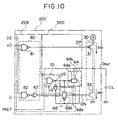
- Fig. 10 is a circuit diagram of a fourth embodiment of the output circuit according to the present invention.
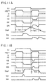
- Fig. 11A is an operating waveform diagram of the output circuit of Fig. 10, in which the output capacitance is a large load capacitance
- Fig. 11B is an operating waveform diagram of the output circuit of Fig. 10, in which the output capacitance is a small load capacitance.
- Fig. 12 is a circuit diagram of a fifth embodiment of the output circuit according to the present invention.
- Fig. 13A is an operating waveform diagram of the output circuit of Fig. 12, in which the output capacitance is a large load capacitance
- Fig. 13B is an operating waveform diagram of the output circuit of Fig. 12, in which the output capacitance is a small load capacitance.
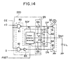
- Fig. 14 is a schematic circuit diagram of a sixth embodiment of the output circuit according to the present invention.
- Fig. 15 is a circuit diagram showing details of the output circuit of Fig. 14.
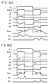
- Fig. 16A is an operating waveform diagram of the output circuit of Fig. 15, in which the output capacitance is a large load capacitance
- Fig. 16B is an operating waveform diagram of the output circuit of Fig. 15, in which the output capacitance is a small load capacitance.
- Fig. 17 is a circuit diagram of a seventh embodiment of the output circuit according to the present invention.
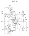
- Fig. 18 is a circuit diagram of an eighth embodiment of the output circuit according to the present invention.
- Fig. 19 is a circuit diagram of a ninth embodiment of the output circuit according to the present invention.
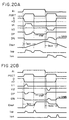
- Fig. 20A is an operating waveform diagram of the output circuit of Fig. 19, in which the output capacitance is a large load capacitance
- Fig. 20B is an operating waveform diagram of the output circuit of Fig. 19, in which the output capacitance is a small load capacitance.
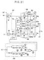
- Fig. 21 is a circuit diagram of a tenth embodiment of the output circuit according to the present invention.
- Fig. 22A is an operating waveform diagram of the output circuit of Fig. 21, in which the output capacitance is a large load capacitance
- Fig. 22B is an operating waveform diagram of the output circuit of Fig. 21, in which the output capacitance is a small load capacitance.
- Fig. 23A is a circuit diagram showing the semiconductor device output circuit of prior art 1
- Fig. 23B is a circuit diagram of a portion of the output circuit of Fig. 23A showing the transistors which operate during presetting.
- Fig. 24A is an operating waveform diagram of the output circuit of Fig. 23A, in which the output capacitance is a small load capacitance
- Fig. 24B is an operating waveform diagram of the output circuit of Fig. 23A, in which the output capacitance is a large load capacitance.
- Fig. 25 is a circuit diagram showing the semiconductor device output circuit of prior art 2.
- Fig. 26A is an operating waveform diagram of the output circuit of Fig. 25, in which the output capacitance is a large load capacitance
- Fig. 26B is an operating waveform diagram of the output circuit of Fig. 25, in which the output capacitance is a small load capacitance.
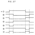
- Fig. 27 is an operating waveform diagram showing the operation of an address transition detection circuit of the output circuit of Fig. 21.
- the semiconductor memory device such as a RAM, has as shown in Fig. 1 a memory cell array 1 which is laid out in a matrix, and includes bit lines and word lines not shown in the figure.
- the signals from the memory cell pass through the column gate 4 and are amplified by a sense amplifier 5, then output to I/O by an output circuit 10.
- a control section 6 enables operation of the sense amplifier 5 and output circuit 10.
- signals from I/O are subject to data processing in a write control section 7, and are transferred to a data bus (DB), and at the same time through the WL decoder 2 and column gate 4, the word lines and bit lines are selected, and data is written to a memory cell. At this time, the sense amplifier 5 and output circuit 10 are inhibited by the control section 6.
- the configuration excludes the above-mentioned configuration necessary for writing.
- the output circuit of the present invention is a circuit which sets the output terminal D out to a predetermined potential intermediate between the power supply line potential and ground line potential before data signals D and xD are output.
- the output circuit includes an output drive means 30, output preset transistor circuit 40, a shorting means 50 and a setting means 22A.
- the output drive means 30 includes a Pch transistor 31 being a first transistor connected to a power supply line and the output terminal D out , and an Nch transistor 32 being a second transistor connected to a ground line and the output terminal D out .
- the transistors 31 and 32 output data signals D and xD from the output terminal D out based on first and second control signals input to first and second control terminals such as a gate electrode DP and a gate electrode DN.
- the output preset transistor circuit 40 is connected to the output terminal D out and at least one of the power supply line and ground line, and serves to set the output terminal D out to a potential intermediate between the power supply line potential and ground line potential.
- the output preset transistor circuit 40 comprises a Pch transistor 41 as a first preset transistor connected to the output terminal D out and a power supply line. It further comprises an Nch transistor 42 as a second preset transistor, of opposite conductivity type to the first preset transistor, connected to the output terminal D out and a ground line.
- the shorting means 50A has the function, after setting (of the transistors 31 and 32 to the off state) by the setting means 22A during the emission of pulses as described below, of, according to the potential state of the output terminal D out , shorting at least one of the control terminals (for example, the gate electrode GP and gate electrode GN) of the output preset transistor circuit 40, and the output terminal D out .
- the shorting means 50A includes a switch means 60 and output potential detection means 70.
- the switch means 60 is connected between the output terminal D out and the gate electrodes of the output preset transistor circuit 40.
- the switch means 60 further comprises a first switch 62 connected between the gate electrode GP being a third control terminal of the Pch transistor 41 and the output terminal D out .
- a second switch 64 connected between the gate electrode GN being a fourth control terminal of the Nch transistor 42 and the output terminal D out .
- the first switch 62 is constituted as a transmission gate comprising a Pch transistor 62a and Nch transistor 62b.
- the second switch 64 is constituted as a transmission gate comprising a Pch transistor 64a and Nch transistor 64b.
- the output potential detection means 70 detects the output terminal potential, and has the function of controlling this switch means 60 based on this detected output potential.
- the output potential detection means 70 comprises a NOR gate 71 and inverter 72 which control the first switch 62 according to the potential of the output terminal D out .
- it comprises a NAND gate 73 and inverter 74 which control the second switch 64 according to the potential of the output terminal D out .
- the NOR gate 71 and NAND gate 73 are controlled by a preset control signal PSET.
- PSET When the preset control signal PSET is low, the first and second switches 62 and 64 become non-conducting, and when the preset control signal PSET is high, according to the potential level of the output terminal D out , one of the first and second switch means 62 and 64 becomes conducting.
- the setting means 22A has the function of controlling control signals (such as the signals DP and DN shown in Fig. 3A) input to the gate electrodes DP and DN of transistors 31 and 32 before the data signals D and xD which are the output from sense amplifiers, and for example during the emission of a pulse of the preset control signal PSET which is a pulse signal which is generated consequent on the detection of a change in the address signals Ai (for example, in the interval which is high in Fig. 3A), and of setting the transistors 31 and 32 to the off state.
- This setting means 22A includes an output control means 80.
- the output control means 80 inputs control signals to the gate electrodes DP and DN of transistors 31 and 32, thereby serving to control the transistors 31 and 32 of the output drive means 30.
- the output control means 80 has a NAND gate 82 and an inverter 83 which control the Nch transistor 32 based on internal data D and output control signals OE. And it has a NAND gate 81 which controls the Pch transistor 31 based on internal data xD and output control signals OE.
- Fig. 3 is a timing chart showing operating waveforms of the circuit of Fig. 2, and also shows current waveforms I op and I on of the output drive means and current waveforms I psp and I psn of the output preset transistor.
- Fig. 3A shows the case where the output capacitance C L is a large load capacitance of 100 pF or more
- Fig. 3B shows the case where C L is a small load capacitance of several picofarads.
- an output potential detection means 70 is activated, and the potential level of the output terminal D out is determined.
- the gate electrode GP of the Pch transistor 41 and the output terminal D out being a drain electrode are shorted, and are then at the same potential. For this reason, since the output terminal D out has a higher capacitance (100 pF) than the gate electrode GP (generally several picofarads), the gate electrode GP is pulled down to approximately 0 V.
- the Pch transistor 41 becomes conducting (on), and by means of the current I psp the output terminal D out begins to rise.
- the characteristics of the Pch transistor 41 are as shown in Fig. 4B.
- the characteristics of the Pch transistor are such as when the output terminal D out is at 0 V to be "on”, and when "on", as the potential of the output terminal D out rises, the voltage between the gate and source of the Pch transistor 41 falls, as a result of which the current drive ability (referred to hereinafter as "ability") is reduced.
- ability the current drive ability
- the second switch 64 does not conduct, and the Nch transistor 42 also does not conduct.
- the output terminal D out is set to an intermediate potential. Thereafter, reflecting a new address an internal data signal xD not shown in the figure goes high, the Pch transistor 31 goes on, and the output terminal D out rises to the power supply potential (Step A6).
- an output potential detection means 70 is activated, and the potential level of the output terminal D out is determined.
- the gate electrode GN of the Nch transistor 42 and the output terminal D out being a drain electrode are shorted, and are then at the same potential. For this reason, since the output terminal D out has a higher capacitance (100 pF) than the gate electrode GN (generally several picofarads), the gate electrode GP is pulled up to approximately the power supply potential.
- the Nch transistor 42 becomes conducting (on), and by means of the current I psn the output terminal D out begins to fall. Since the output terminal D out and GN are at the same potential, the potential of the gate electrode GN also falls together with the output terminal D out (Step B3).
- the characteristics of the Nch transistor 42 are as shown in Fig. 4E.
- the characteristics of the Nch transistor are such as when the output terminal D out is at the power supply voltage to be "on”, and when "on", as the potential of the output terminal D out falls, the voltage between the gate and source of the Nch transistor 42 falls, as a result of which the power is reduced. It should be noted that close to the threshold value the current is low. Therefore, the current I psn is reduced, and the degree of falling of the output terminal D out is reduced (Step B4).
- Step B5 the second switch 64 becomes non-conducting, the gate potential GN goes to 0 V by virtue of the transistor 92, the Nch transistor 42 goes off, and the preset operation is stopped.
- the first switch 62 does not conduct, and the Pch transistor 41 also does not conduct.
- the output terminal D out is set to an intermediate potential. Thereafter, reflecting a new address an internal data signal D not shown in the figure goes high, the Nch transistor 32 goes on, and the output terminal D out falls to 0 V (Step B6).
- the first switch 62 becomes conducting.
- the gate electrode GP and the output terminal D out reach the same potential, but since the terminal capacitance of the output terminal D out and the gate electrode GP capacitance are approximately the same, the output terminal D out goes to an intermediate potential determined by the capacitance ratio of the output terminal D out and gate electrode GP.
- step A3 sine the Pch transistor 41 goes on, the output terminal D out rises.
- Step A5 even when the preset control signal PSET is high, if the potential of the output terminal D out goes to the logic level of the NOR gate 71 or more, the first switch 62 is non-conducting, the potential of the gate electrode GP goes to the power supply potential, and the Pch transistor 41, with the output terminal D out at the intermediate potential, goes off, and the preset operation is stopped (Step A5).
- the gate electrode GN and the output terminal D out reach the same potential, but since the terminal capacitance of the output terminal D out and the gate electrode GN capacitance are approximately the same, the output terminal D out goes to an intermediate potential determined by the capacitance ratio of the output terminal D out and GN.
- step B3 sine the Nch transistor 42 goes on, the output terminal D out falls.
- step A4 close to the threshold voltage of the Nch transistor 42, the power of the Nch transistor 42 is severely reduced.
- the Nch transistor has characteristics like those shown as I in Fig. 4E, and close to the threshold V th the current is small.
- the discharge rate at the intermediate potential can be made slower than the operation speed of the output potential detection means 70, and before the output terminal has been subject to excessive discharge, the potential state of the output terminal can be detected, so that no oscillation occurs in the output, and erroneous operation of peripheral devices or the like can be prevented.
- Step B5 even when the preset control signal PSET is high, if the potential of the output terminal D out goes to the logic level of the NAND gate 73 or less, the second switch 64 is non-conducting, the potential of the gate electrode GN goes to 0 V, and the Nch transistor 42, with the output terminal D out at the intermediate potential, goes off, and the preset operation is stopped (Step B5).
- step B6 the output terminal D out falls to the ground line potential.
- Fig. 5 shows the relationship between the time to confirm a data value (access time) and the power supply voltage, and shows characteristics of a semiconductor device with a power supply voltage specification of 3 V ⁇ 10% (2.7 to 3.3 V).
- Fig. 5A shows the case with no preset
- Fig. 5B shows the conventional case
- Fig. 5C shows the case of the present embodiment.
- the power supply voltage is 4.0 V or less, then reaccessing is not necessary, and the time to confirm a data value (access time) is also shorter than with a conventional type and than with a type without preset. For this reason, regardless of the load capacitance the noise can be reduced, and high speed access is achieved, which also increases the general-purpose applicability.
- the output circuit in this second embodiment provides, as shown in Fig. 6, a configuration in which an intermediate potential is established only when, in the above-mentioned first embodiment, the output terminal D out changes from high to low.
- the output preset transistor circuit 40 comprises only an Nch transistor 42
- the output potential detection means 70 comprises only a NAND gate 73 and inverter 74
- the switch means 60 comprises only a second switch 64.
- the operating waveforms are the same as in Fig. 3 except for the change from low to high.
- the output preset transistor circuit 40 and shorting means 50B together comprise a potential setting means 20A.
- This potential setting means 20A is connected to the output terminal D out , and serves to lower the voltage of the terminal D out , and set the output terminal D out to a predetermined voltage.
- the potential setting means 20A has input thereto a voltage V which falls over time, and has current - voltage characteristics such that as the voltage V falls the current I falls, and the rate of falling of the current as the voltage falls is, compared with its initial value, later smaller, and moreover, when the input voltage V is close to the threshold voltage V th of the potential setting means 20A, the current I flowing in the potential setting means 20A is small.
- the potential setting means 20A is not restricted to the configuration shown in Fig. 6 above, but essentially may have any configuration which has the characteristics shown in Fig. 4E.
- the time constant can be made large, and the speed of discharge at the intermediate potential can be made slower than the operation speed of the output potential detection means.
- the output circuit in this third embodiment provides, as shown in Fig. 8, a configuration in which an intermediate potential is established only when, in the above-mentioned first embodiment the output terminal D out changes from low to high.
- the output preset transistor circuit 40 comprises only a Pch transistor 41
- the output potential detection means 70 comprises only a NOR gate 71 and inverter 72
- the switch means 60 comprises only a first switch 62.
- the operating waveforms are the same as in Fig. 3 except for the change from high to low.
- the output preset transistor circuit 40 and shorting means 50C together comprise a potential setting means 20B.
- This potential setting means 20B is connected to the output terminal D out , and serves to raise the voltage of the terminal D out , and set the output terminal D out to a predetermined voltage.
- the potential setting means 20B has input thereto a voltage V which rises over time, and has current - voltage characteristics such that as the voltage V rises the current I falls, and the rate of falling of the current as the voltage rises is, compared with its initial value, later smaller, and moreover, when the input voltage V is close to the threshold voltage V th of the potential setting means 20B, the current I flowing in the potential setting means 20B is small.
- the potential setting means 20B is not restricted to the configuration shown in Fig. 8 above, but essentially may have any configuration which has the characteristics shown in Fig. 4B.
- the device of Fig. 10 comprises an output terminal D out and a potential setting means 20C.
- the potential setting means 20C comprises a shorting means 50D and a setting means 22B.
- the shorting means 50D comprises a switch 64 as a first switch means connected between a control terminal gate electrode DN of the second transistor 32 of the output drive means 30 and the output terminal D out . It further comprises an output potential detection means 70 which detects the potential of the output terminal D out , and based on the detected output potential, controls the switch 64.
- the setting means 22B also comprises the output potential detection means 70. Further, it comprises an output control means 80 which by inputting control signals to first and second control terminals such as the gate electrode DP and the gate electrode DN of the first and second transistors 31 and 32 controls the transistors 31 and 32 of the output drive means 30. Further, it comprises a switch 68 being a second switch means, connected between the output control means 80 and the gate electrode DN, and controlled by the output potential detection means 70.
- the output potential detection means 70 is used by both the shorting means 50D and the setting means 22B. Then before data signals D and xD are output, under the control of the output potential detection means 70, the switch 64 is made conducting, and the switch 68 is made non-conducting, and with data input inhibited, the transistor 32 is operated, and the output terminal D out is set to an intermediate potential. It should be noted that the output drive means 30, the output potential detection means 70, the output control means 80, and so forth have the same configuration as in Fig. 6.
- the switch 64 is connected between the output terminal D out and the gate electrode DN of the Nch transistor 32, and is constituted as a transmission gate comprising a Pch transistor 64a and Nch transistor 64b.
- the switch 68 is connected between the gate electrode DN of the Nch transistor 32 which is the second control terminal of the output drive means 30 and the output control means 80, and is constituted as a transmission gate comprising a Pch transistor 68a and Nch transistor 68b.
- the NAND gate 73 is controlled based on a preset control signal PSET. Specifically, when the preset control signal PSET is low, switch 68 is made conducting, and switch means 64 is made non-conducting, and when the preset control signal PSET is high, and moreover the potential of the output terminal D out level is higher than the logic level of the NAND gate 73, the switch 68 is made non-conducting, and the switch 64 is made conducting.
- Fig. 11 is a timing chart showing operating waveforms of the circuit of Fig. 10, and also shows current waveforms I op and I on of the output drive means 30.
- Fig. 11A shows the case where the output capacitance C L is a large load capacitance of 100 pF or more
- Fig. 11B shows the case where C L is a small load capacitance of several picofarads.
- Step C2 In the change from low to high, no preset operation is carried out, and the output terminal D out rises at a speed determined by the output load capacitance and the power of the Pch transistor 31 (Step C2).
- Step D2 Since the output terminal D out is high, the output V 2 of the NAND gate 73 goes low, and switch 68 becomes non-conducting and switch 64 becomes conducting (Step D2).
- the gate electrode DN of the Nch transistor 32 and the output terminal D out which is the drain electrode are shorted to be at the same potential, and the gate electrode DN goes approximately to the power supply potential, as determined by the capacitance ratio between the output terminal D out of 100 pF and the gate electrode DN of several picofarads.
- the Nch transistor 32 becomes conducting, and the output terminal D out begins to fall. Then since the output terminal D out and gate electrode DN are at the same potential, the potential of the gate electrode DN also falls together with the output terminal D out (Step D3).
- Step D4 With the fall in the potential of the output terminal D out , the voltage between the gate and source falls, and therefore the power of the Nch transistor 32 is reduced, and the speed with which the output terminal D out falls is reduced. It should be noted that close to the threshold the current is small (Step D4).
- the gate potential DN goes to ground potential by virtue of the Nch transistor of the inverter 83, the Nch transistor 32 goes off, and preset operation is stopped (Step D5).
- the internal data signal xD is fixed at low, and therefore the Pch transistor 31 does not conduct.
- Step D6 the internal data signal D goes high, and once again the Nch transistor 32 goes on, and the output terminal D out falls.
- switch 68 becomes non-conducting, the switch 64 becomes conducting, and the gate electrode DN and the output terminal D out go to the same potential.
- the output terminal D out terminal capacitance and gate electrode DN have approximately the same capacitance, the output terminal D out goes to an intermediate potential determined by the capacitance ratio of the output terminal D out and the gate electrode DN.
- step D3 the Nch transistor 32 goes on, and therefore the output terminal D out falls.
- step D4 as the potential of the output terminal D out falls, the power of the Nch transistor 32 is reduced, and therefore as the potential becomes lower the rate of change of the output terminal D out potential is reduced.
- Step D5 even when the preset control signal PSET is high, if the potential of the output terminal D out is at or less than the logic level of the NAND gate 73, the switch 64 becomes non-conducting, the switch 68 becomes conducting, the gate potential gate electrode DN is grounded by the inverter 83, the Nch transistor 32 goes off, and the presetting operation is stopped (Step D5).
- step D6 the output terminal D out falls to the ground line potential.
- a fifth embodiment of the present invention is described with reference to Figs. 12 and 13.
- This embodiment is the reverse of the fourth embodiment, providing a Pch transistor only, for the case only that the output terminal D out goes from low to high. Therefore, since configuration, benefits and so forth are similar to those of the fourth embodiment, detailed description is omitted here.
- Fig. 14 is a circuit diagram of an output circuit showing schematically the sixth embodiment of the present invention.
- the output circuit comprises a shorting means 50F, and a setting means 22D.
- the shorting means 50F comprises a first switch means 61 connected between the output terminal D out and the gate electrode DP and gate electrode DN which are the first and second control terminals of the first and second transistors 31 and 32 of the output drive means 30. Further, shorting means 50F comprises an output potential detection means 70 which detects the potential of the output terminal D out , and based on the detected output potential controls the first switch means 61.
- the setting means 22D comprises the output potential detection means 70 and an output control means 80 which by inputting output control signals to control terminal gate electrode DP and gate electrode DN of the first and second transistors 31 and 32, controls transistors 31 and 32. Further, setting means 22D comprises a second switch means 65, connected between the output control means 80 and the control terminal gate electrode DP and gate electrode DN, and controlled by the output potential detection means 70.
- first switch means 61 are used first and second switches 62 and 64, and as the second switch means 65 are used third and fourth switches 66 and 68.
- the first switch 62 is connected between the output terminal D out and the gate electrode DP of the Pch transistor 31.
- the second switch 64 is connected between the output terminal D out and the gate electrode DN of the Nch transistor 32.
- the third switch 66 is connected between the gate electrode DP of the Pch transistor 31 and the output control means 80.
- the fourth switch 68 is connected between the gate electrode DN of the Nch transistor 32 and the output control means 80.
- the output potential detection means 70 controls the first to fourth switches 62, 64, 66, and 68 by means of the preset control signal PSET and the potential of the output terminal D out .
- the output potential detection means 70 is used in common by the shorting means 50F and setting means 22D. Moreover, before the data signals D and xD are output, either of the upper and lower switches 62 and 64 of the first switch means 61 is made conducting, and either of the upper and lower switches 66 and 68 of the second switch means 65 is made non-conducting by the output potential detection means 70, and in the data input inhibited state, one of the transistors 31 and 32 is operated, to set the output terminal D out to an intermediate potential. It should be noted that the output drive means 30, the output potential detection means 70, the output control means 80 and so forth have the same configuration as in Fig. 2.
- Fig. 15 is a circuit diagram of the output circuit showing the sixth embodiment of the present invention
- the switches 62, 64, 66, and 68 in the circuit in Fig. 14 are constituted by Pch transistors (62a, 64a, 66a, and 68a) and Nch transistors (62b, 64b, 66b, and 68b) as transmission gates
- the output potential detection means 70 has the same configuration as the output potential detection means 70 in the circuit diagram shown in Fig. 2.
- the NOR gate 71 and NAND 73 are controlled by the preset control signal PSET, and when the preset control signal PSET is low, switches 62 and 64 are non-conducting, switches 66 and 68 are conducting, and the output drive means 30 is under the control of the output control means 80.
- Fig. 16 is a timing chart showing operating waveforms of the circuit of Fig. 15, and also shows current waveforms I op and I on of the output drive means.
- Fig. 16A shows the operating waveforms in the case where the output capacitance C L is a large load capacitance of 100 pF or more, and Fig. 16B in the case where C L is a small load capacitance of several picofarads.
- the gate electrode DP of the Pch transistor 31 and the output terminal D out are shorted, and at the same potential, and by virtue of the capacitance ratio of 100 pF for the output terminal D out to several picofarads for the gate electrode DP, the gate electrode DP is substantially at 0 V.
- the Pch transistor 31 goes on, the output terminal D out begins to rise, and by virtue of the first switch 62, since the output terminal D out and the gate electrode DP are at the same potential, the gate electrode DP potential also rises together with the output terminal D out .
- the first switch 62 becomes conducting, the second switch 64 remains non-conducting, and the gate electrode DP and output terminal D out go to the same potential.
- the output terminal D out in this case the terminal capacitance only
- the gate electrode DP have approximately the same capacitance, and therefore the output terminal D out and the gate electrode DP go to an intermediate potential determined by the capacitance ratio.
- the speed with which the output terminal D out rises does not exceed the operation speed of the output potential detection means 70.
- the preset control signal PSET is high, if the potential of the output terminal D out is at least at the logic level of the NOR gate 71, the first switch 62 becomes non-conducting, the gate potential DP goes to the power supply potential, and with the output terminal D out at the intermediate potential the Pch transistor 31 stops the presetting operation.
- the second switch 64 When the output terminal D out potential goes from high to low, the second switch 64 becomes conducting, by virtue of the Nch transistor 32 an intermediate potential is preset, and thereafter once again the Nch transistor 32 operates, and is pulled down to the ground line potential.
- a seventh embodiment of the present invention is described with reference to Figs. 16 and 17.
- the difference between this embodiment and the above-mentioned sixth embodiment is a difference in the first to fourth switches 62, 64, 66, and 68, and in the output control means 80.
- the first switch 62 is connected between the output terminal D out and the gate electrode of the Pch transistor 31, and uses an Nch transistor, of opposite conductivity type to the Pch transistor 31.
- the second switch 64 is connected between the output terminal D out and the gate electrode of the Nch transistor 32, and uses a Pch transistor, of opposite conductivity type to the Nch transistor 32.
- the third switch 66 is connected between the control terminal gate electrode DP of the Pch transistor 31 and the output control means 80.
- the fourth switch 68 is connected between the gate electrode DN being the second control terminal of the Nch transistor 32 and the output control means 80.
- the output control means 80 comprises a NAND 82 and transistors 86 and 87 which control the Nch transistor 32 in accordance with the internal data signal D and output control signals OE. And it comprises a NAND 81, inverter 83, and transistors 84 and 85 which control the Pch transistor 31 in accordance with the internal data signal xD and output control signals OE.
- the output potential detection means 70 is the same as in Fig. 15, and the control operation of the first to fourth switches 62, 64, 66, and 68 according to the preset control signal PSET and the potential of the output terminal D out level is also the same as in Fig. 15.
- the transistors 84 and 85 form together with the third switch 66 a clocked inverter.
- the transistors 86 and 87 form together with the fourth switch means 68 a clocked inverter.
- the clocked inverter including the NAND 81, the inverter 83, and the third switch 66 is equivalent to the NAND 81 and third switch 66 in the circuit of Fig. 15.
- the clocked inverter including the NAND 82 and the fourth switch 68 is equivalent to the NAND 82, the inverter 83, and the fourth switch 68 in the circuit of Fig. 15.
- circuit operation of the seventh embodiment shown in Fig. 17 is basically the same as the operation of the circuit shown in Fig. 15 and only the points of difference are described.
- the back gate effect on the Nch transistor 32 is small. Additionally, the voltage between the gate and source is also large. For this reason, the operation of the Nch transistor 32 is not restricted, and it is conducting.
- the threshold voltage of the Nch transistor 62 is modulated by the back gate effect, and its degree of conducting is restricted. Therefore, the voltage of the gate electrode DP does not rise above the power supply voltage reduced by a threshold voltage including the back gate effect of the Nch transistor 62. However, since the output terminal D out is at the intermediate potential, a presetting operation is not required.
- the presetting operation is carried out in the same way as in the circuit of Fig. 15, and the operating waveforms of the Fig. 17 circuit are the same as shown in the timing chart of Fig. 16.
- the above seventh embodiment provides the following benefits.
- the circuit in Fig. 18 eliminates the Nch transistor 66b of the third switch 66 and the Pch transistor 68a of the fourth switch 68 from the circuit of Fig. 17, and also eliminates the inverters 72 and 74 from the output potential detection means 70, but otherwise is the same circuit configuration as in Fig. 7.
- the output V 1 of the NOR 71 is low, the first switch 66 is conducting, and the Pch transistor 84 also is conducting by virtue of the internal data signal xD being low, and therefore the gate electrode DP goes high, and during the presetting interval the Pch transistor 31 does not go on.
- Fig. 19 is a circuit diagram showing a ninth embodiment of the output circuit of the present invention.
- Fig. 19 differs from the circuit of Fig. 18 in that the Pch transistor 66 of the third switch 66 and the Nch transistor 68 of the fourth switch 68 are connected in series to the control terminal of the output drive means 30 and the output of the output control means 80, and the output control means 80 comprises NANDs 81 and 82 and inverter 83.
- Fig. 20 is a timing chart showing operating waveforms of the circuit shown in Fig. 19, and also shows current waveforms I op and I on of the output drive means.
- Fig. 20A shows the operating waveforms in the case where the output capacitance C L is a large load capacitance of 100 pF or more, and Fig. 20B in the case where C L is a small load capacitance.
- the gate potential does not rise to the power supply voltage, and the potential is reduced by the threshold voltage V thn of the Nch transistor 68.
- the gate potential of the Pch transistor 31 is restricted by the threshold voltage of the third switch 66. At this time, by making the size of the transistors 31 and 32 appropriate to provide the desired power, it is possible to avoid any effect on accessing.
- the presetting interval for example when the output terminal D out is high, the output V 1 of the NOR 71 is low, and the switch means 66 is conducting, the internal data signal xD is low, and the output of the NAND 81 is high, and therefore the gate electrode DP goes high, and during the presetting interval the Pch transistor 31 does not go on.
- a tenth embodiment of the present invention is described with reference to Figs. 21 and 22.
- the preset control signal PSET of the above embodiments is employed the logic of a transition detection circuit (ATD) 100 which is the internal clock signal of an asynchronous memory device, for example. Therefore, the effect and benefit is the same as in the above-mentioned embodiments.
- the operating waveforms of the address transition detection circuit are as shown in Fig. 27.
- the amount of change of the current of the preset transistor or the output drive means (di/dt: the larger this value the larger the voltage effect of the parasitic inductance, and the larger the noise.) is affected by the power of the switch connected between the output terminal and the output preset transistor or output drive means gate terminal, and can easily be adjusted by the size of the switch means.
- the amount of change of the current, in other words the noise, at the start of presetting can be adjusted.
- the preset control signal PSET may employ an external clock signal of a synchronous semiconductor device, or may employ a signal which detects changes in an external clock signal.
- the timing of the internal data signals D and xD is different from that in a conventional device, as shown in Fig. 26, but during the presetting operation when the preset control signal PSET goes high, for example, an address transition detection signal ATD may be used to easily control the operation of a sense amplifier.
- the power supply voltage is made high, fast access and low noise operation are possible, so that the range of usable power supply voltage is substantially increased compared with the conventional case, and use as an output circuit of wide applicability, for example to a gate array, random logic output circuit, microprocessor, control IC, or electronic instrument, is possible.
- the emission of noise from the output circuit itself can be reduced, and therefore, for example, in a semiconductor memory device including the output circuit, the causing by noise emission of erroneous operation of other ICs or other components mounted on the same board is avoided.
- switches, output drive means, and the like in place of MOS transistors may equally be used bipolar transistors.
- the output drive means may equally by of an open-drain type, and as 31 in Fig. 10 may equally be used an Nch transistor.
Landscapes
- Engineering & Computer Science (AREA)
- Computer Hardware Design (AREA)
- Physics & Mathematics (AREA)
- Computing Systems (AREA)
- General Engineering & Computer Science (AREA)
- Mathematical Physics (AREA)
- Power Engineering (AREA)
- Microelectronics & Electronic Packaging (AREA)
- Logic Circuits (AREA)
- Electronic Switches (AREA)
- Dram (AREA)
- Static Random-Access Memory (AREA)
- Direct Current Feeding And Distribution (AREA)
Applications Claiming Priority (4)
| Application Number | Priority Date | Filing Date | Title |
|---|---|---|---|
| JP172626/95 | 1995-07-07 | ||
| JP17262695 | 1995-07-07 | ||
| JP17262695 | 1995-07-07 | ||
| PCT/JP1996/001851 WO1997003498A1 (fr) | 1995-07-07 | 1996-07-04 | Circuit de sortie et dispositif electronique utilisant ledit circuit |
Publications (3)
| Publication Number | Publication Date |
|---|---|
| EP0780984A1 true EP0780984A1 (fr) | 1997-06-25 |
| EP0780984A4 EP0780984A4 (fr) | 1998-09-16 |
| EP0780984B1 EP0780984B1 (fr) | 2003-11-12 |
Family
ID=15945372
Family Applications (1)
| Application Number | Title | Priority Date | Filing Date |
|---|---|---|---|
| EP96922222A Expired - Lifetime EP0780984B1 (fr) | 1995-07-07 | 1996-07-04 | Circuit de sortie et dispositif electronique utilisant ledit circuit |
Country Status (8)
| Country | Link |
|---|---|
| US (1) | US6018256A (fr) |
| EP (1) | EP0780984B1 (fr) |
| JP (1) | JP3551432B2 (fr) |
| KR (1) | KR100253717B1 (fr) |
| CN (1) | CN1099761C (fr) |
| DE (1) | DE69630658T2 (fr) |
| TW (1) | TW352488B (fr) |
| WO (1) | WO1997003498A1 (fr) |
Cited By (1)
| Publication number | Priority date | Publication date | Assignee | Title |
|---|---|---|---|---|
| DE19651548C2 (de) * | 1995-12-21 | 2001-07-12 | Lg Semicon Co Ltd | CMOS-Ausgangsschaltung mit einer Ladevorspannungsschaltung |
Families Citing this family (11)
| Publication number | Priority date | Publication date | Assignee | Title |
|---|---|---|---|---|
| JP2000156084A (ja) * | 1998-11-19 | 2000-06-06 | Fujitsu Ltd | 半導体装置 |
| US6184730B1 (en) * | 1999-11-03 | 2001-02-06 | Pericom Semiconductor Corp. | CMOS output buffer with negative feedback dynamic-drive control and dual P,N active-termination transmission gates |
| US6351159B1 (en) | 2000-08-08 | 2002-02-26 | Micron Technology, Inc. | Gate coupled voltage support for an output driver circuit |
| US7551007B2 (en) * | 2005-02-11 | 2009-06-23 | Fairchild Semiconductor Corporation | Partial switch gate driver |
| US8384444B1 (en) * | 2005-09-03 | 2013-02-26 | Texas Instruments Incorporated | I/O driver with pass gate feedback controlled output driver |
| US9252764B1 (en) * | 2013-03-12 | 2016-02-02 | Cirrus Logic, Inc. | Systems and methods for reducing spike voltages in a switched output stage |
| US9847706B2 (en) | 2013-03-14 | 2017-12-19 | Cirrus Logic, Inc. | Systems and methods for reducing voltage ringing in a power converter |
| US8872561B2 (en) | 2013-03-14 | 2014-10-28 | Cirrus Logic, Inc. | Systems and methods for edge control based on detecting current direction in a switched output stage |
| US8970258B2 (en) | 2013-03-14 | 2015-03-03 | Cirrus Logic, Inc. | Systems and methods for edge control in a switched output stage |
| US9171609B2 (en) * | 2013-12-04 | 2015-10-27 | Integrated Silicon Solution (Shanghai), Inc. | Address transition detecting circuit |
| CN113141176B (zh) * | 2020-01-17 | 2024-12-24 | 江森自控空调冷冻设备(无锡)有限公司 | 自动配置输出电路 |
Family Cites Families (14)
| Publication number | Priority date | Publication date | Assignee | Title |
|---|---|---|---|---|
| JP2548700B2 (ja) * | 1986-01-08 | 1996-10-30 | 三菱電機株式会社 | 半導体集積回路 |
| JPS63112893A (ja) * | 1986-10-28 | 1988-05-17 | Mitsubishi Electric Corp | 半導体集積回路 |
| JPS63117839A (ja) * | 1986-11-07 | 1988-05-21 | Hirota Tekkosho:Kk | 折丁等の供給装置 |
| JPH0817037B2 (ja) * | 1987-12-03 | 1996-02-21 | 松下電子工業株式会社 | スタティックramの出力回路 |
| KR910002748B1 (ko) * | 1988-04-12 | 1991-05-04 | 삼성 반도체통신 주식회사 | 반도체장치에 있어서 데이타 출력 버퍼회로 |
| JP2767834B2 (ja) * | 1988-10-21 | 1998-06-18 | セイコーエプソン株式会社 | 半導体記憶装置 |
| DE69019551T2 (de) * | 1989-02-18 | 1995-09-21 | Sony Corp | Speicheranordnungen. |
| JPH02220294A (ja) * | 1989-02-21 | 1990-09-03 | Sony Corp | 半導体装置における出力回路 |
| JP2895500B2 (ja) * | 1989-03-08 | 1999-05-24 | 沖電気工業株式会社 | Mos型出力バッファ回路 |
| JPH04281298A (ja) * | 1991-01-08 | 1992-10-06 | Nec Corp | Eprom装置 |
| JPH05189974A (ja) * | 1992-01-13 | 1993-07-30 | Mitsubishi Electric Corp | 出力バッファ回路 |
| JPH07135463A (ja) * | 1993-11-12 | 1995-05-23 | Sony Corp | プリコンディショニング回路 |
| DE4400872A1 (de) * | 1994-01-14 | 1995-07-20 | Philips Patentverwaltung | Ausgangstreiberschaltung |
| JPH0877775A (ja) * | 1994-08-31 | 1996-03-22 | Nkk Corp | データ出力回路 |
-
1996
- 1996-07-04 CN CN96190719A patent/CN1099761C/zh not_active Expired - Fee Related
- 1996-07-04 WO PCT/JP1996/001851 patent/WO1997003498A1/fr not_active Ceased
- 1996-07-04 DE DE69630658T patent/DE69630658T2/de not_active Expired - Fee Related
- 1996-07-04 EP EP96922222A patent/EP0780984B1/fr not_active Expired - Lifetime
- 1996-07-04 US US08/809,895 patent/US6018256A/en not_active Expired - Lifetime
- 1996-07-04 KR KR1019970701492A patent/KR100253717B1/ko not_active Expired - Fee Related
- 1996-07-04 JP JP50566397A patent/JP3551432B2/ja not_active Expired - Fee Related
- 1996-10-17 TW TW085112696A patent/TW352488B/zh not_active IP Right Cessation
Cited By (1)
| Publication number | Priority date | Publication date | Assignee | Title |
|---|---|---|---|---|
| DE19651548C2 (de) * | 1995-12-21 | 2001-07-12 | Lg Semicon Co Ltd | CMOS-Ausgangsschaltung mit einer Ladevorspannungsschaltung |
Also Published As
| Publication number | Publication date |
|---|---|
| US6018256A (en) | 2000-01-25 |
| KR970705868A (ko) | 1997-10-09 |
| KR100253717B1 (ko) | 2000-04-15 |
| TW352488B (en) | 1999-02-11 |
| HK1017826A1 (en) | 1999-11-26 |
| EP0780984A4 (fr) | 1998-09-16 |
| JP3551432B2 (ja) | 2004-08-04 |
| DE69630658D1 (de) | 2003-12-18 |
| WO1997003498A1 (fr) | 1997-01-30 |
| EP0780984B1 (fr) | 2003-11-12 |
| CN1099761C (zh) | 2003-01-22 |
| CN1158192A (zh) | 1997-08-27 |
| DE69630658T2 (de) | 2004-10-07 |
Similar Documents
| Publication | Publication Date | Title |
|---|---|---|
| KR0132504B1 (ko) | 데이타 출력버퍼 | |
| US4918339A (en) | Data output circuit | |
| JP3320565B2 (ja) | 出力回路および動作方法 | |
| EP0301603B1 (fr) | Circuit de sortie de dispositif de circuit intégré à semi-conducteurs | |
| US20010052796A1 (en) | Output circuit for a transmission system | |
| US6792372B2 (en) | Method and apparatus for independent output driver calibration | |
| US6018256A (en) | Output circuit and electronic apparatus using the same | |
| US5805505A (en) | Circuit and method for converting a pair of input signals into a level-limited output signal | |
| US5367205A (en) | High speed output buffer with reduced voltage bounce and no cross current | |
| KR950007449B1 (ko) | 메모리의 출력 버퍼 회로 | |
| US6060905A (en) | Variable voltage, variable impedance CMOS off-chip driver and receiver interface and circuits | |
| JPWO1997003498A1 (ja) | 出力回路及びそれを用いた電子機器 | |
| US6996010B2 (en) | Fast-sensing amplifier for flash memory | |
| US4019068A (en) | Low power output disable circuit for random access memory | |
| US8604828B1 (en) | Variable voltage CMOS off-chip driver and receiver circuits | |
| HK1017826B (en) | Output circuit and electronic device using the circuit | |
| US5668769A (en) | Memory device performance by delayed power-down | |
| US7046562B2 (en) | Integrated circuit reset circuitry | |
| US6331786B1 (en) | Termination circuits and methods therefor | |
| US6084444A (en) | Buffer driver reference circuit | |
| JP3105808B2 (ja) | 半導体装置およびこの半導体装置のモード設定方法 | |
| JP3745875B2 (ja) | 半導体メモリ装置のバーンインストレス制御回路 | |
| JP2930014B2 (ja) | オープンドレイン電流制御回路 | |
| JP2753560B2 (ja) | 出力バッファ回路 | |
| JPH10125069A (ja) | 半導体メモリ |
Legal Events
| Date | Code | Title | Description |
|---|---|---|---|
| PUAI | Public reference made under article 153(3) epc to a published international application that has entered the european phase |
Free format text: ORIGINAL CODE: 0009012 |
|
| 17P | Request for examination filed |
Effective date: 19970305 |
|
| AK | Designated contracting states |
Kind code of ref document: A1 Designated state(s): DE FI FR GB |
|
| A4 | Supplementary search report drawn up and despatched |
Effective date: 19980724 |
|
| AK | Designated contracting states |
Kind code of ref document: A4 Designated state(s): DE FI FR GB |
|
| 17Q | First examination report despatched |
Effective date: 20020724 |
|
| GRAH | Despatch of communication of intention to grant a patent |
Free format text: ORIGINAL CODE: EPIDOS IGRA |
|
| GRAS | Grant fee paid |
Free format text: ORIGINAL CODE: EPIDOSNIGR3 |
|
| GRAA | (expected) grant |
Free format text: ORIGINAL CODE: 0009210 |
|
| AK | Designated contracting states |
Kind code of ref document: B1 Designated state(s): DE FI FR GB |
|
| REG | Reference to a national code |
Ref country code: GB Ref legal event code: FG4D |
|
| REF | Corresponds to: |
Ref document number: 69630658 Country of ref document: DE Date of ref document: 20031218 Kind code of ref document: P |
|
| ET | Fr: translation filed | ||
| PLBE | No opposition filed within time limit |
Free format text: ORIGINAL CODE: 0009261 |
|
| STAA | Information on the status of an ep patent application or granted ep patent |
Free format text: STATUS: NO OPPOSITION FILED WITHIN TIME LIMIT |
|
| 26N | No opposition filed |
Effective date: 20040813 |
|
| REG | Reference to a national code |
Ref country code: HK Ref legal event code: GR Ref document number: 1017826 Country of ref document: HK |
|
| PGFP | Annual fee paid to national office [announced via postgrant information from national office to epo] |
Ref country code: FR Payment date: 20090710 Year of fee payment: 14 |
|
| PGFP | Annual fee paid to national office [announced via postgrant information from national office to epo] |
Ref country code: GB Payment date: 20090701 Year of fee payment: 14 Ref country code: FI Payment date: 20090716 Year of fee payment: 14 Ref country code: DE Payment date: 20090702 Year of fee payment: 14 |
|
| GBPC | Gb: european patent ceased through non-payment of renewal fee |
Effective date: 20100704 |
|
| REG | Reference to a national code |
Ref country code: FR Ref legal event code: ST Effective date: 20110331 |
|
| PG25 | Lapsed in a contracting state [announced via postgrant information from national office to epo] |
Ref country code: DE Free format text: LAPSE BECAUSE OF NON-PAYMENT OF DUE FEES Effective date: 20110201 |
|
| REG | Reference to a national code |
Ref country code: DE Ref legal event code: R119 Ref document number: 69630658 Country of ref document: DE Effective date: 20110201 |
|
| PG25 | Lapsed in a contracting state [announced via postgrant information from national office to epo] |
Ref country code: FR Free format text: LAPSE BECAUSE OF NON-PAYMENT OF DUE FEES Effective date: 20100802 Ref country code: FI Free format text: LAPSE BECAUSE OF NON-PAYMENT OF DUE FEES Effective date: 20100704 |
|
| PG25 | Lapsed in a contracting state [announced via postgrant information from national office to epo] |
Ref country code: GB Free format text: LAPSE BECAUSE OF NON-PAYMENT OF DUE FEES Effective date: 20100704 |