EP0781012A2 - Rechenwerk - Google Patents
Rechenwerk Download PDFInfo
- Publication number
- EP0781012A2 EP0781012A2 EP96309261A EP96309261A EP0781012A2 EP 0781012 A2 EP0781012 A2 EP 0781012A2 EP 96309261 A EP96309261 A EP 96309261A EP 96309261 A EP96309261 A EP 96309261A EP 0781012 A2 EP0781012 A2 EP 0781012A2
- Authority
- EP
- European Patent Office
- Prior art keywords
- instruction
- voice
- demodulating
- modulating
- synchronizing
- Prior art date
- Legal status (The legal status is an assumption and is not a legal conclusion. Google has not performed a legal analysis and makes no representation as to the accuracy of the status listed.)
- Withdrawn
Links
Images


Classifications
-
- H—ELECTRICITY
- H04—ELECTRIC COMMUNICATION TECHNIQUE
- H04L—TRANSMISSION OF DIGITAL INFORMATION, e.g. TELEGRAPHIC COMMUNICATION
- H04L27/00—Modulated-carrier systems
- H04L27/18—Phase-modulated carrier systems, i.e. using phase-shift keying
- H04L27/22—Demodulator circuits; Receiver circuits
- H04L27/233—Demodulator circuits; Receiver circuits using non-coherent demodulation
- H04L27/2338—Demodulator circuits; Receiver circuits using non-coherent demodulation using sampling
Definitions
- the present invention relates to an arithmetic unit, and particularly to an arithmetic unit adapted to a processor for audio communication or digital signal processing.
- Processors for voice communication and digital signal processing generally use pipelining for executing a plurality of instructions simultaneously in overlapping (as described, for example, in "COMPUTER ARCHITECHTURE A QUANTITATIVE APPROACH SECOND EDTION", Chapter 3, written by John L. Hennessy and David A. Patterson).
- arithmetic ability can be improved by subdividing the pipelining into pipeline stages (processing units) so as to increase the number of instructions to be executed simultaneously. Further, because the number of logic stages per pipeline stage can be reduced, the operating rate can be improved.
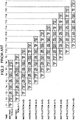
- the arithmetic unit has a program counter 1 for indicating an access address of an instruction memory 2, the instruction memory 2 for storing instruction data, an instruction-memory-data storage means 3 for storing instruction data which is given from the instruction memory 2, and a first instruction decoder 4 for decoding instruction data which is given from the instruction-memory-data storage means 3 and outputting a data memory address and a result of temporary decoding of an instruction (hereinafter referred to as "an instruction-temporary-decoded-result").
- the arithmetic unit further has a data-memory-address storage means 5 for holding the data memory address given from the first instruction decoder 4, a data memory 6 which is accessed on the basis of the data memory address given from the data-memory-address storage means 5 and in which an output data is stored, and a data-memory-data storage means 7 for holding the output data given from the data memory 6.
- the arithmetic unit further has a storage means 8 for holding the instruction-temporary-decoded-result given from the first instruction decoder 4, a second instruction decoder 9 for decoding the instruction-temporary-decoded-result given from the storage means 8, a storage means 10 for holding the decoded result of the second instruction decoder 9, an arithmetic portion 11 for performing an arithmetic operation for the output data given from the data-memory-data storage means 7 on the basis of contents indicated by the decoded result given from the storage means 10, and a storage means 12 for holding the arithmetic result given from the arithmetic portion 11.
- an address is outputted from the program counter 1 to the instruction memory 2 and then the value of the program counter 1 is incremented by one (pre-IF stage for instruction i ).
- an instruction data stored in the address which is given from the program counter 1 to the instruction memory 2 at time T1 is outputted from the instruction memory 2 to the instruction-memory-data storage means 3 and held in the instruction-memory-data storage means 3 (post-IF stage for instruction i ).
- pipeline latches may be provided in the inside of the instruction memory 2 or a wave pipeline configuration is used in the instruction memory 2 in order to separate an IF stage into a pre-IF stage and a post-IF stage.
- a plurality of waves for data propagation are disposed among storage devices by performing clocking at a rate higher than the propagation delay of a combination circuit (JP-A-7-93149).
- the instruction data held in the instruction-memory-data storage means 3 at time T2 is decoded by the first instruction decoder 4 to thereby generate a data memory address and an instruction-temporary-decoded-result to be used in the next DEC2 stage (pre-DEC1 stage for instruction i ).
- the data memory address and the instruction-temporary-decoded-result generated at time T3 are held in the data-memory-address storage means 5 and the storage means 8 respectively (post-DEC1 stage for instruction i+1).
- pipeline latches may be provided in the inside of the first instruction decoder 4 or a wave pipeline configuration may be used in the first instruction decoder 4 in order to separate a DEC1 stage into a pre-DEC1 stage and a post-DEC1 stage.
- the instruction data stored in the address which is given from the program counter 1 to the instruction memory 2 at time T2 is outputted from the instruction memory 2 to the instruction-memory-data storage means 3 and held in the instruction-memory-data storage means 3 (post-IF stage for instruction i+1) and, at the same time, an address is outputted from the program counter 1 to the instruction memory 2 and then the value of the program counter 1 is incremented by one (pre-IF stage for instruction i+2).
- the instruction data held in the instruction-memory-data storage means 3 at time T3 is decoded by the first instruction decoder 4 to thereby generate a data memory address and an instruction-temporary-decoded-result to be used in the next DEC2 stage (pre-DEC1 stage for instruction i+1).
- the instruction data stored in the address which is given from the program counter 1 to the instruction memory 2 at time T3 is outputted from the instruction memory 2 to the instruction-memory-data storage means 3 and held in the instruction-memory-data storage means 3 (post-IF stage for instruction i+2) and, at the same time, an address is outputted from the program counter 1 to the instruction memory 2 and then the value of the program counter 1 is incremented by one (pre-IF stage for instruction i+3).
- the data memory 6 is accessed on the basis of the data memory address which is outputted from the data-memory-address storage means 5 and, at the same time, the instruction-temporary-decoded-result held in the storage means 8 at time T4, is decoded by the second instruction decoder 9 into a signal format which is necessary for the next EX stage (pre-DEC2 stage for instruction i ).
- the output data from the data memory 6 is held in the data-memory-data storage means 7 and, at the same time, the data decoded by the second instruction decoder 9 is held in the storage means 10 (post-DEC2 stage for instruction i ).
- pipeline latches may be provided in the inside of the data memory 6 and the second instruction decoder 9 or a wave pipeline configuration may be used in the data memory 6 and the second instruction decoder 9 in order to separate a DEC2 stage into a pre-DEC2 stage and a post-DEC2 stage.
- the data memory address and the instruction-temporary-decoded-result generated by the first instruction decoder 4 at time T4 are held in the data-memory-address storage means 5 and the storage means 8 respectively (post-DEC1 stage for instruction i+1).
- the instruction data held in the instruction-memory-data storage means 3 at time T4 is decoded by the first instruction decoder 4 to thereby generate a data memory address and an instruction-temporary-decoded-result to be used in the next DEC2 stage (pre-DEC1 stage for instruction i+2).
- the instruction data stored in the address which is given from the program counter 1 to the instruction memory 2 at time T4 is outputted from the instruction memory 2 to the instruction-memory-data storage means 3 and held in the instruction-memory-data storage means 3 (post-IF stage for instruction i+3) and, at the same time, an address is outputted from the program counter 1 to the instruction memory 2 and then the value of the program counter 1 is incremented by one (pre-IF stage for instruction i+4).
- the data memory 6 is accessed on the basis of the data memory address which is outputted from the data-memory-address storage means 5 and, at the same time, the instruction-temporary-decoded-result held in the storage means 8 at time T5 is decoded by the second instruction decoder 9 into a signal format which is necessary for the next EX stage (pre-DEC2 stage for instruction i+1).
- the data memory address and the instruction-temporary-decoded-result generated by the first instruction decoder 4 at time T5 are held in the data-memory-address storage means 5 and the storage means 8 respectively (post-DEC1 stage for instruction i+2).
- the instruction data held in the instruction-memory-data storage means 3 at time T5 is decoded by the first instruction decoder 4 to thereby generate a data memory address and an instruction-temporary-decoded-result to be used for the next DEC2 stage (pre-DEC1 stage for instruction i+3).
- the instruction data stored in the address which is given from the program counter 1 to the instruction memory 2 at time T5 is outputted from the instruction memory 2 to the instruction-memory-data storage means 3 and held in the instruction-memory-data storage means 3 (post-IF stage for instruction i+4) and, at the same time, an address is outputted from the program counter 1 to the instruction memory 2 and then the value of the program counter 1 is incremented by one (pre-IF stage for instruction i+5).
- the arithmetic portion 11 performs an arithmetic operation for the output data from the data-memory-data storage means 7 on the basis of contents designated by the output signal of the storage means 10 (pre-EX stage for instruction i ).
- the arithmetic result in the arithmetic portion 11 is held in the storage means 12 (post-EX stage for instruction i ).
- pipeline latches may be provided in the inside of the arithmetic portion 11 or a wave pipeline configuration may be used in the arithmetic portion 11 in order to separate an EX stage into a pre-EX stage and a post-EX stage.
- the output data from the data memory 6 is held in the data-memory-data storage means 7 and, at the same time, the data decoded by the second instruction decoder 9 at time T6 is held in the storage means 10 (post-DEC2 stage for instruction i+1).
- the data memory 6 is accessed on the basis of the data memory address outputted from the data-memory-address storage means 5 and, at the same time, the instruction-temporary-decoded-result held in the storage means 8 at time T6 is decoded by the second instruction decoder 9 into a signal format which is necessary for the next EX stage (pre-DEC2 stage for instruction i+2).
- the data memory address and the instruction-temporary-decoded-result generated by the first instruction decoder 4 at time T6 are held in the data-memory-address storage means 5 and the storage means 8 respectively (post-DEC1 stage for instruction i+3).
- the instruction data held in the instruction-memory-data storage means 3 at time T6 is decoded by the first instruction decoder 4 to thereby generate a data memory address and an instruction-temporary-decoded-result to be used in the next DEC2 stage (pre-DEC1 stage for instruction i+4).
- the instruction data stored in the address which is given from the program counter 1 to the instruction memory 2 at time T6 is outputted from the instruction memory 2 to the instruction-memory-data storage means 3 and held in the instruction-memory-data storage means 3 (post-IF stage for instruction i+5) and, at the same time, an address is outputted from the program counter 1 to the instruction memory 2 and then the value of the program counter 1 is incremented by one (pre-IF stage for instruction i+6).
- the arithmetic portion 11 performs an arithmetic operation for the output data from the data-memory-data storage means 7 on the basis of contents designated by the output signal of the storage means 10 (pre-EX stage for instruction i+1).
- the output data from the data memory 6 is held in the data-memory-data storage means 7 and, at the same time, the data decoded by the second instruction decoder 9 is held in the storage means 10 (post-DEC2 stage for instruction i+2).
- the data memory 6 is accessed on the basis of the data memory address outputted from the data-memory-address storage means 5 and, at the same time, the instruction-temporary-decoded-result held in the storage means 8 at time T7 is decoded by the second instruction decoder 9 into a signal format which is necessary for the next EX stage (pre-DEC2 stage for instruction i+3).
- the data memory address and the instruction-temporary-decoded-result generated by the first instruction decoder 4 at time T7 are held in the data-memory-address storage means 5 and the storage means 8 respectively (post-DEC1 stage for instruction i+4).
- the instruction data held in the instruction-memory-data storage means 3 at time T7 is decoded by the first instruction decoder 4 to thereby generate a data memory address and an instruction-temporary-decoded-result to be used in the next DEC2 stage (pre-DEC1 stage for instruction i+5).
- the instruction data stored in the address which is given from the program counter 1 to the instruction memory 2 at time T7 is outputted from the instruction memory 2 to the instruction-memory-data storage means 3 and held in the instruction-memory-data storage means 3 (post-IF stage for instruction i+6) and, at the same time, an address is outputted from the program counter 1 to the instruction memory 2 and then the value of the program counter 1 is incremented by one (pre-IF stage for instruction i+7).
- a post-EX stage for instruction i As described above, at time T8 in Fig. 2, a post-EX stage for instruction i , a pre-EX stage for instruction i+1, a post-DEC2 stage for instruction i+2, a pre-DEC2 stage for instruction i+3, a post-DEC1 stage for instruction i+4, a pre-DEC1 stage for instruction i+5, a post-IF stage for instruction i+6 and a pre-IF stage for instruction i+7 are executed simultaneously. As a result, there can be provided eight-fold performance compared with the case where the respective stages for the instructions are executed one by one.
- the processor having the aforementioned conventional pipeline configuration has the following problems.
- An object of the present invention is to provide an arithmetic unit in which pipelines can be used effectively and, accordingly, arithmetic ability can be improved.
- an arithmetic unit for performing a demodulating operation for a received signal, a synchronizing operation based on a demodulated signal, a voice decoding operation for the demodulated signal, a voice encoding operation for a voice, and a modulating operation for a coded voice by a pipeline processing method comprises:
- an arithmetic unit for performing a demodulating operation for a received signal, a synchronizing operation based on a demodulated signal, a voice decoding operation for the demodulated signal, a voice encoding operation for a voice and a modulating operation for a coded voice by a pipeline processing method, comprises:
- an arithmetic unit for performing a demodulating operation for a received signal, a synchronizing operation based on a demodulated signal, a voice decoding operation for the demodulated signal, a voice encoding operation for a voice and a modulating operation for a coded voice by a pipeline processing method, comprises:
- an arithmetic unit for performing a demodulating operation for a received signal, a synchronizing operation based on a demodulated signal, a voice decoding operation for the demodulated signal, a voice encoding operation for a voice and a modulating operation for a coded voice by a pipeline processing method, comprises:
- an arithmetic unit for performing a demodulating operation for a received signal, a synchronizing operation based on a demodulated signal, a voice decoding operation for the demodulated signal, a voice encoding operation for a voice and a modulating operation for a coded voice by a pipeline processing method, comprises:
- an arithmetic unit for performing a demodulating operation for a received signal, a synchronizing operation based on a demodulated signal, a voice decoding operation for the demodulated signal, a voice encoding operation for a voice and a modulating operation for a coded voice by a pipeline processing method, comprises:
- an arithmetic unit provided with a pipeline configuration for executing n instruction sequences successively, comprises:
- a mobile communication apparatus depicted in Fig. 4 comprises an RF portion 21 for processing a high-frequency-band signal, a demodulation portion 22 for demodulating an output signal of the RF portion 21, a synchronization portion 23 for performing synchronization on the basis of an output signal of the demodulation portion 22, an voice decoding portion 24 for voice-decoding the output signal of the demodulation portion 22, a speaker 25 for reproducing a voice decoded by the voice decoding portion 24, a microphone 26, a voice encoding portion 27 for encoding a voice inputted through the microphone 26, and a modulation portion 28 for modulating coded data inputted through the voice encoding portion 27.
- instructions contained in processing in the voice decoding portion 24 and processing in the voice encoding portion 27 are called “voice encoding/decoding instructions” and instructions contained in processing in the demodulation portion 22, processing in the synchronization portion 23 and processing in the modulation portion 28 are called “modulating/demodulating/synchronizing instructions”.
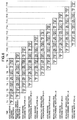
- Fig. 5 shows an arithmetic unit according to an embodiment of the present invention in which pipelines of two instruction sequences of voice encoding/decoding instructions and modulating/demodulating/synchronizing instructions flow.
- the arithmetic unit in this embodiment has first and second program counters 101 and 101a for indicating access addresses of an instruction memory 102 which will be described later.
- the first and second program counters 101 and 101a are used to be alternated every instruction.
- the first program counter 101 is used for executing voice encoding/decoding instructions and the second program counter 101a is used for executing modulating/demodulating/synchronizing instructions.
- the arithmetic unit further has an instruction memory 102 in which instruction data are stored, and first and second instruction-memory-data storage portions 103 and 103a in which instruction data outputted from the instruction memory 102 are held.
- the first and second instruction-memory-data storage portions 103 and 103a are used to be alternated every instruction.
- the first instruction-memory-data storage portion 103 is used for executing voice encoding/decoding instructions
- the second instruction-memory-data storage portion 103a is used for executing modulating/demodulating/synchronizing instructions.
- the arithmetic unit further has a first instruction decoder 104 for decoding instruction data given from the first and second instruction-memory-data storage portions 103 and 103a and outputting data memory addresses and instruction-temporary-decoded-results, and first and second data-memory-address storage portions 105 and 105a for holding the data memory addresses given from the first instruction decoder 104.
- the first and second data-memory-address storage portions 105 and 105a are used to be alternated every instruction.
- the first data-memory-address storage portion 105 is used for executing voice encoding/decoding instructions and the second data-memory-address storage portion 105a is used for executing modulating/demodulating/synchronizing instructions.
- the arithmetic unit further has a data memory 106 which is accessed on the basis of the addresses given from the first and second data-memory-address storage portions 105 and 105a and in which output data are stored, and first and second data-memory-data storage portions 107 and 107a for holding the output data given from the data memory 106.
- the first and second data-memory-data storage portions 107 and 107a are used to be alternated every instruction. Specifically, the first data-memory-data storage portion 107 is used for executing voice encoding/decoding instructions and the second data-memory-data storage portion 107a is used for executing modulating/demodulating/synchronizing instructions.
- the arithmetic unit further has first and second storage portions 108 and 108a for holding the instruction-temporary-decoded-results given from the first instruction decoder 104.
- the first and second storage portions 108 and 108a are used to be alternated every instruction. Specifically, the first storage portion 108 is used for executing voice encoding/decoding instructions and the second storage portion 108a is used for executing modulating/demodulating/synchronizing instructions.
- the arithmetic unit further has a second instruction decoder 109 for decoding the instruction-temporary-decoded-results given from the first and second storage portions 108 and 108a, and third and fourth storage portions 110 and 110a for holding the decoded results given from the second instruction decoder 109.
- the third and fourth storage portions 110 and 110a are used to be alternated every instruction. Specifically, the third storage portion 110 is used for executing voice encoding/decoding instructions and the fourth storage portion 110a is used for executing modulating/demodulating/synchronizing instructions.
- the arithmetic unit further has an arithmetic portion 111 for performing an arithmetic operation for output data given from the first and second data-memory-data storage portions 107 and 107a, on the basis of contents designated by the decoded results which are given from the third and fourth storage portions 110 and 110a, and fifth and sixth storage portions 112 and 112a for holding arithmetic results which are given from the arithmetic portion 111.
- the fifth and sixth storage portions 112 and 112a are used to be alternated every instruction. Specifically, the fifth storage portion 112 is used for executing voice encoding/decoding instructions and the sixth storage portion 112a is used for executing modulating/demodulating/synchronizing instructions.
- Fig. 5 is a pipeline configuration view.
- an address is outputted from the first program counter 101 to the instruction memory 102 and then the value of the first program counter 101 is incremented by one (pre-IF stage for voice encoding/decoding instruction i ).
- an instruction data stored in the address which is given from the first program counter 101 to the instruction memory 102 at time T1 is outputted from the instruction memory 102 to the first instruction-memory-data storage portion 103 and held in the first instruction-memory-data storage portion 103 (post-IF stage for voice encoding/decoding instruction i ).
- pipeline latches may be provided in the inside of the instruction memory 102 or a wave pipeline configuration may be used in the instruction memory 102 in order to separate an IF stage into a pre-IF stage and a post-IF stage.
- an address is outputted from the second program counter 101a to the instruction memory 102 and then the value of the second program counter 101a is incremented by one (pre-IF stage for modulating/demodulating/synchronizing instruction j ).
- the instruction data held in the first instruction-memory-data storage portion 103 at time T2 is decoded by the first instruction decoder 104 to thereby generate a data memory address and an instruction-temporary-decoded-result to be used in the next DEC2 stage (pre-DEC1 stage for voice encoding/decoding instruction i ).
- the data memory address and the instruction-temporary-decoded-result generated by the first instruction decoder 104 at time T3 are stored in the first data memory address storage portion 105 and the first storage portion 108 respectively (post-DEC1 stage for voice encoding/decoding instruction i ).
- pipeline latches may be provided in the inside of the first instruction decoder 104 or a wave pipeline configuration may be used in the first instruction decoder 104 in order to separate a DEC1 stage into a pre-DEC1 stage and a post-DEC1 stage.
- the instruction data stored in the address which is given from the second program counter 101a to the instruction memory 102 at time T2 is outputted from the instruction memory 102 to the second instruction-memory-data storage portion 103a and held in the second instruction-memory-data storage portion 103a (post-IF stage for modulating/demodulating/synchronizing instruction j ) and, at the same time, an address is outputted from the first program counter 101 to the instruction memory 102 and then the value of the first program counter 101 is incremented by one (pre-IF stage for voice encoding/decoding instruction i+1).
- the instruction data held in the second instruction-memory-data storage portion 103a at time T3 is decoded by the first instruction decoder 104 to thereby generate a data memory address and an instruction-temporary-decoded-result to be used in the next DEC2 stage (pre-DEC1 stage for modulating/demodulating/synchronizing instruction j ).
- the instruction data held in the address which is given from the first program counter 101 to the instruction memory 102 at time T3 is outputted from the instruction memory 102 to the first instruction-memory-data storage portion 103 and held in the first instruction-memory-data storage portion 103 (post-IF stage for voice encoding/decoding instruction i+1) and, at the same time, an address is outputted from the second program counter 101a to the instruction memory 102 and then the value of the second program counter 101a is incremented by one (pre-IF stage for modulating/demodulating/synchronizing instruction j+1).
- the data memory 106 is accessed on the basis of the data memory address which is outputted from the first data memory address storage portion 105 and, at the same time, the instruction-temporary-decoded-result held in the first storage portion 108 at time T4 is decoded by the second instruction decoder 109 into a signal format which is necessary for the next EX stage (pre-DEC2 stage for voice encoding/decoding instruction i ).
- the output data from the data memory 106 is held in the first data-memory-data storage portion 107 and, at the same time, the data decoded by the second instruction decoder 109 is held in the third storage portion 110 (post-DEC2 stage for voice encoding/decoding instruction i ).
- pipeline latches may be provided in the inside of the data memory 106 and the second instruction decoder 109 or a wave pipeline configuration may be used in the data memory 106 and the second instruction decoder 109 in order to separate a DEC2 stage into a pre-DEC2 stage and a post-DEC2 stage.
- the data memory address and the instruction-temporary-decoded-result generated by the first instruction decoder 104 at time T4 are held in the second data memory address storage portion 105a and the second storage portion 108a respectively (post-DEC1 stage for modulating/demodulating/synchronizing instruction j ).
- the instruction data held in the first instruction-memory-data storage portion 103 at time T4 is decoded by the first instruction decoder 104 to thereby generate a data memory address and an instruction-temporary-decoded-result to be used in the next DEC2 stage (pre-DEC1 stage for voice encoding/decoding instruction i+1).
- the instruction data stored in the address which is given from the second program counter 101a to the instruction memory 102 at time T4 is outputted from the instruction memory 102 to the second instruction-memory-data storage portion 103a and held in the second instruction-memory-data storage portion 103a (post-IF stage for modulating/demodulating/synchronizing instruction j+1) and, at the same time, an address is outputted from the first program counter 101 to the instruction memory 102 and then the value of the first program counter 101 is incremented by one (pre-IF stage for voice encoding/decoding instruction i+2).
- the data memory 106 is accessed on the basis of the data memory address which is outputted from the second data memory address storage portion 105a and, at the same time, the instruction-temporary-decoded-result held in the second storage portion 108a at time T5 is decoded by the second instruction decoder 109 into a signal format which is necessary for the next EX stage (pre-DEC2 stage for modulating/demodulating/synchronizing instruction j ).
- the data memory address and the instruction-temporary-decoded-result generated by the first instruction decoder 104 at time T5 are held in the first data memory address storage portion 105 and the first storage portion 108 respectively (post-DEC1 stage for voice encoding/decoding instruction i+1).
- the instruction data held in the second instruction-memory-data storage portion 103a at time T5 is decoded by the first instruction decoder 104 to thereby generate a data memory address and an instruction-temporary-decoded-result to be used in the next DEC2 stage (pre-DEC1 stage for modulating/demodulating/synchronizing instruction j+1).
- the instruction data stored in the address which is given from the first program counter 101 to the instruction memory 102 at time T5 is outputted from the instruction memory 102 to the first instruction-memory-data storage portion 103 and held in the first instruction-memory-data storage portion 103 (post-IF stage for voice encoding/decoding instruction i+2) and, at the same time, an address is outputted from the second program counter 101a to the instruction memory 102 and then the value of the second program counter 101a is incremented by one (pre-IF stage for modulating/demodulating/synchronizing instruction j+2).
- the arithmetic portion 111 performs an arithmetic operation for the output data from the first data-memory-data storage portion 107 on the basis of contents designated by the output signal of the third storage portion 110 (pre-EX stage for voice encoding/decoding instruction i ).
- the arithmetic result in the arithmetic portion 111 is held in the fifth storage portion 112 (post-EX stage for voice encoding/decoding instruction i ).
- pipeline latches may be provided in the inside of the arithmetic portion 111 or a wave pipeline configuration may be used in the arithmetic portion 111 in order to separate an EX stage into a pre-EX stage and a post-EX stage.
- the output data from the data memory 106 is held in the second data-memory-data storage portion 107a and, at the same time, the data decoded by the second instruction decoder 109 at time T6 is held in the fourth storage portion 110a (post-DEC2 stage for modulating/demodulating/synchronizing instruction j ).
- the data memory 106 is accessed on the basis of the data memory address outputted from the first data memory address storage portion 105 and, at the same time, the instruction-temporary-decoded-result held in the first storage portion 108 at time T6 is decoded by the second instruction decoder 109 into a signal format which is necessary for the next EX stage (pre-DEC2 stage for voice encoding/decoding instruction i+1).
- the data memory address and the instruction-temporary-decoded-result generated by the first instruction decoder 104 at time T6 are held in the second data memory address storage portion 105a and the second storage portion 108a respectively (post-DEC1 stage for modulating/demodulating/synchronizing instruction j+1).
- the data instruction held in the first instruction-memory-data storage portion 103 at time T6 is decoded by the first instruction decoder 104 to thereby generate a data memory address and an instruction-temporary-decoded-result to be used in the next DEC2 stage (pre-DEC1 stage for voice encoding/decoding instruction i+2).
- the instruction data stored in the address which is given from the second program counter 101a to the instruction memory 102 at time T6 is outputted from the instruction memory 102 to the second instruction-memory-data storage portion 103a and held in the second instruction-memory-data storage portion 103a (post-IF stage for modulating/demodulating/synchronizing instruction j+2) and, at the same time, an address is outputted from the first program counter 101 to the instruction memory 102 and then the value of the first program counter 101 is incremented by one (pre-IF stage for voice encoding/decoding instruction i+3).
- the arithmetic portion 111 performs an arithmetic operation for the output data from the second data-memory-data storage portion 107a on the basis of contents designated by the output signal of the fourth storage portion 110a (pre-EX stage for modulating/demodulating/synchronizing instruction j ).
- the output data from the data memory 106 is held in the first data-memory-data storage portion 107 and, at the same time, the data decoded by the second instruction decoder 109 is held in the third storage portion 110 (post-DEC2 stage for voice encoding/decoding instruction i+1).
- the data memory 106 is accessed on the basis of the data memory address which is outputted from the second data memory address storage portion 105a and, at the same time, the instruction-temporary-decoded-result held in the second storage portion 108a at time T7 is decoded by the second instruction decoder 109 into a signal format which is necessary for the next EX stage (pre-DEC2 stage for modulating/demodulating/synchronizing instruction j+1).
- the data memory address and the instruction-temporary-decoded-result generated by the first instruction decoder 104 at time T7 are held in the first data memory address storage portion 105 and the first storage portion 108 respectively (post-DEC1 stage for voice encoding/decoding instruction i+2).
- the instruction data held in the second instruction-memory-data storage portion 103a at time T7 is decoded by the first instruction decoder 104 to thereby generate a data memory address and an instruction-temporary-decoded-result to be used in the next DEC2 stage (pre-DEC1 stage for modulating/demodulating/synchronizing instruction j+2).
- the instruction data stored in the address which is given from the first program counter 101 to the instruction memory 102 at time T7 is outputted from the instruction memory 102 to the first instruction-memory-data storage portion 103 and held in the first instruction-memory-data storage portion 103 (post-IF stage for voice encoding/decoding instruction i+3) and, at the same time, an address is outputted from the second program counter 101a to the instruction memory 102 and then the value of the second program counter 101a is incremented by one (pre-IF stage for modulating/demodulating/synchronizing instruction j+3).
- Fig. 7 is a pipeline configuration view.
- Fig. 7 shows the case where a branch instruction occurs in a modulating/demodulating/synchronizing instruction
- this rule can be also applied to the case where a branch instruction occurs in a voice encoding/decoding instruction. That is, even in the case where a branch instruction occurs in a voice encoding/decoding instruction, the time of occurrence of stalling can be reduced because stalling does not occur in modulating/demodulating/synchronizing instructions but it occurs only in voice encoding/decoding instructions.
- the voice encoding/decoding instruction i is an instruction which is such that the arithmetic result is determined after the post-EX stage is completed.
- the post-EX stage for the voice encoding/decoding instruction i is completed (time T8). Accordingly, the voice encoding/decoding instruction i+1 can use the arithmetic result of the voice encoding/decoding instruction i .
- modulating/demodulating/synchronizing instruction j+1 can use the arithmetic result of modulating/demodulating/synchronizing instruction j .
- pipelines can be used effectively even in the case where instructions using the previous arithmetic result are inputted continuously.
- voice encoding and demodulation require a larger deal of processing.
- modulation, voice decoding and synchronization require a smaller deal of processing. Therefore, the quantities of processing required for two instruction sequences can be equalized by separating instructions into a voice encoding/decoding instruction sequence and a modulating/demodulating/synchronizing instruction sequence so that the two instruction sequences flow.
- voice encoding can be started immediately after modulation or voice demodulation can be started immediately after demodulation. Accordingly, there arises an advantage that the delay of processing can be shortened.
- the delay of processing can be also shortened as described above.
- the quantities of processing can be made uniform by adding synchronization to one of groups of (modulation + voice encoding) and (demodulation + voice decoding) which is smaller in the quantity of processing.
- timing control in signal processing can be made more accurately because synchronization can be made continuously. Furthermore, as described above, in this separation method, the delay of processing can be shortened.
- timing control in signal processing can be made more accurately because synchronization can be made continuously as described above. Furthermore, this separation method is adapted to team development because development can be made while separated into development by voice signal processing developers and development by modulation/demodulation signal processing developers as described above.
- JP-A-5-298093 As an apparatus for processing a plurality of instructions simultaneously in the same manner as in the present invention, there is a processing apparatus disclosed in JP-A-5-298093.
- this JP-A-5-298093 there is description about a method for compensating for lowering of processing efficiency in a branch instruction in the processing apparatus but there is no description about a plurality of programs to be executed.
- the present invention is different from the conventional processing apparatus in the configuration concerning the allocation of a plurality of instruction sequences in a communication apparatus and the advantages thereof.
- the embodiment according to the present invention has the following advantages which are not mentioned in JP-A-5-298093.
- pipelines can be used effectively even in the case where a branch instruction occurs, so that pipelines can be used effectively even in the case where instructions using previous arithmetic results are inputted continuously. Accordingly, because lowering of arithmetic ability is avoided even in the case where pipelines are taken deeply, pipelines can be taken deeply so that the operating rate can be improved. Furthermore, because software development can be allotted to technical experts in accordance with their special fields by an idea of separation of processing, the present invention is adapted to program development by team. Furthermore, not only the delay of processing can be shortened by the idea of separation of processing but also timing control can be made more accurately by the idea of separation of processing. Accordingly, an arithmetic unit of high performance can be provided.
Landscapes
- Engineering & Computer Science (AREA)
- Computer Networks & Wireless Communication (AREA)
- Signal Processing (AREA)
- Advance Control (AREA)
- Complex Calculations (AREA)
- Compression, Expansion, Code Conversion, And Decoders (AREA)
- Reduction Or Emphasis Of Bandwidth Of Signals (AREA)
- Transmission Systems Not Characterized By The Medium Used For Transmission (AREA)
Applications Claiming Priority (3)
| Application Number | Priority Date | Filing Date | Title |
|---|---|---|---|
| JP331434/95 | 1995-12-20 | ||
| JP33143495 | 1995-12-20 | ||
| JP7331434A JPH09171462A (ja) | 1995-12-20 | 1995-12-20 | 演算装置 |
Publications (2)
| Publication Number | Publication Date |
|---|---|
| EP0781012A2 true EP0781012A2 (de) | 1997-06-25 |
| EP0781012A3 EP0781012A3 (de) | 2000-10-11 |
Family
ID=18243629
Family Applications (1)
| Application Number | Title | Priority Date | Filing Date |
|---|---|---|---|
| EP96309261A Withdrawn EP0781012A3 (de) | 1995-12-20 | 1996-12-19 | Rechenwerk |
Country Status (3)
| Country | Link |
|---|---|
| US (1) | US5930518A (de) |
| EP (1) | EP0781012A3 (de) |
| JP (1) | JPH09171462A (de) |
Families Citing this family (5)
| Publication number | Priority date | Publication date | Assignee | Title |
|---|---|---|---|---|
| US6963961B1 (en) * | 2001-07-09 | 2005-11-08 | Lsi Logic Corporation | Increasing DSP efficiency by independent issuance of store address and data |
| JP2006215292A (ja) * | 2005-02-04 | 2006-08-17 | Renesas Technology Corp | オーディオデータ処理装置 |
| US8195922B2 (en) | 2005-03-18 | 2012-06-05 | Marvell World Trade, Ltd. | System for dynamically allocating processing time to multiple threads |
| US20060212853A1 (en) * | 2005-03-18 | 2006-09-21 | Marvell World Trade Ltd. | Real-time control apparatus having a multi-thread processor |
| JP2012133637A (ja) * | 2010-12-22 | 2012-07-12 | On Semiconductor Trading Ltd | 命令実行回路 |
Citations (2)
| Publication number | Priority date | Publication date | Assignee | Title |
|---|---|---|---|---|
| JPH05298093A (ja) | 1992-04-17 | 1993-11-12 | Hitachi Ltd | 処理装置 |
| JPH0793149A (ja) | 1993-08-31 | 1995-04-07 | Nec Corp | マイクロプロセッサ |
Family Cites Families (9)
| Publication number | Priority date | Publication date | Assignee | Title |
|---|---|---|---|---|
| US5131008A (en) * | 1989-04-28 | 1992-07-14 | Motorola, Inc. | DSP-based GMSK coherent detector |
| JP2749456B2 (ja) * | 1991-03-06 | 1998-05-13 | 三菱電機株式会社 | 無線通信機 |
| US5357617A (en) * | 1991-11-22 | 1994-10-18 | International Business Machines Corporation | Method and apparatus for substantially concurrent multiple instruction thread processing by a single pipeline processor |
| US5319573A (en) * | 1992-01-15 | 1994-06-07 | Motorola, Inc. | Method and apparatus for noise burst detection in a signal processor |
| US5282197A (en) * | 1992-05-15 | 1994-01-25 | International Business Machines | Low frequency audio sub-channel embedded signalling |
| JPH06250856A (ja) * | 1993-02-26 | 1994-09-09 | Nippondenso Co Ltd | マイクロコンピュータ |
| US6304957B1 (en) * | 1993-02-26 | 2001-10-16 | Nippondenso Co., Ltd. | Multitask processing unit |
| US5519640A (en) * | 1994-01-26 | 1996-05-21 | Hughes Aircraft Company | Multimedia frame relay codec |
| US5517436A (en) * | 1994-06-07 | 1996-05-14 | Andreas; David C. | Digital signal processor for audio applications |
-
1995
- 1995-12-20 JP JP7331434A patent/JPH09171462A/ja active Pending
-
1996
- 1996-12-19 US US08/769,419 patent/US5930518A/en not_active Expired - Lifetime
- 1996-12-19 EP EP96309261A patent/EP0781012A3/de not_active Withdrawn
Patent Citations (2)
| Publication number | Priority date | Publication date | Assignee | Title |
|---|---|---|---|---|
| JPH05298093A (ja) | 1992-04-17 | 1993-11-12 | Hitachi Ltd | 処理装置 |
| JPH0793149A (ja) | 1993-08-31 | 1995-04-07 | Nec Corp | マイクロプロセッサ |
Also Published As
| Publication number | Publication date |
|---|---|
| US5930518A (en) | 1999-07-27 |
| EP0781012A3 (de) | 2000-10-11 |
| JPH09171462A (ja) | 1997-06-30 |
Similar Documents
| Publication | Publication Date | Title |
|---|---|---|
| JP3984786B2 (ja) | 異なる待ち時間を伴う命令のスケジューリング | |
| EP2259190A2 (de) | Mehrfach-thread-prozessor mit effizienter verarbeitung für konvergenzeinrichtungsanwendungen | |
| EP0220682B1 (de) | Datenverarbeitungssystem | |
| US20030195645A1 (en) | Circuits and methods for extracting a clock from a biphase encoded bit stream and systems using the same | |
| US7080239B2 (en) | Loop control circuit and loop control method | |
| US5930518A (en) | Arithmetic unit | |
| EP0196964B1 (de) | System zum Einstellen der Leistung einer Informationsverarbeitungsvorrichtung | |
| US20080215859A1 (en) | Computer with high-speed context switching | |
| JP4138180B2 (ja) | プロセッサ | |
| KR20200018238A (ko) | 정보 처리 방법 및 처리 장치 | |
| CN117827284A (zh) | 向量处理器访存指令处理方法、系统、设备及存储介质 | |
| JP3526492B2 (ja) | 並列処理システム | |
| JPS5913762B2 (ja) | 情報バス制御装置 | |
| CN112437303B (zh) | 一种jpeg解码方法及装置 | |
| JPS5896345A (ja) | 階層型演算方式 | |
| CN119322600B (zh) | 浮点数处理方法及装置、电子设备和存储介质 | |
| JP3531856B2 (ja) | プログラム制御方法及びプログラム制御装置 | |
| CN115114051B (zh) | 节点通信方法、装置、设备及存储介质 | |
| US6460129B1 (en) | Pipeline operation method and pipeline operation device to interlock the translation of instructions based on the operation of a non-pipeline operation unit | |
| JP2001344100A (ja) | 複数のフラグレジスタを備えた中央演算処理装置 | |
| JPH04353923A (ja) | 電子計算機の並列命令実行方式 | |
| US20090013159A1 (en) | Queue Processor And Data Processing Method By The Queue Processor | |
| JP2776261B2 (ja) | 計算装置の同期方法 | |
| JPH09319863A (ja) | 画像処理装置における設定データ変更装置 | |
| CN119065718A (zh) | 数据处理方法及处理器 |
Legal Events
| Date | Code | Title | Description |
|---|---|---|---|
| PUAI | Public reference made under article 153(3) epc to a published international application that has entered the european phase |
Free format text: ORIGINAL CODE: 0009012 |
|
| 17P | Request for examination filed |
Effective date: 19961231 |
|
| AK | Designated contracting states |
Kind code of ref document: A2 Designated state(s): DE FR GB |
|
| PUAL | Search report despatched |
Free format text: ORIGINAL CODE: 0009013 |
|
| AK | Designated contracting states |
Kind code of ref document: A3 Designated state(s): DE FR GB |
|
| 17Q | First examination report despatched |
Effective date: 20010315 |
|
| STAA | Information on the status of an ep patent application or granted ep patent |
Free format text: STATUS: THE APPLICATION IS DEEMED TO BE WITHDRAWN |
|
| 18D | Application deemed to be withdrawn |
Effective date: 20020115 |