EP0782039A2 - Dispositif d'affichage et son procédé de fabrication - Google Patents
Dispositif d'affichage et son procédé de fabrication Download PDFInfo
- Publication number
- EP0782039A2 EP0782039A2 EP96309541A EP96309541A EP0782039A2 EP 0782039 A2 EP0782039 A2 EP 0782039A2 EP 96309541 A EP96309541 A EP 96309541A EP 96309541 A EP96309541 A EP 96309541A EP 0782039 A2 EP0782039 A2 EP 0782039A2
- Authority
- EP
- European Patent Office
- Prior art keywords
- film
- liquid crystal
- color filter
- substrates
- tin oxide
- Prior art date
- Legal status (The legal status is an assumption and is not a legal conclusion. Google has not performed a legal analysis and makes no representation as to the accuracy of the status listed.)
- Withdrawn
Links
- 238000000034 method Methods 0.000 title claims description 96
- 239000000758 substrate Substances 0.000 claims abstract description 74
- PJXISJQVUVHSOJ-UHFFFAOYSA-N indium(iii) oxide Chemical compound [O-2].[O-2].[O-2].[In+3].[In+3] PJXISJQVUVHSOJ-UHFFFAOYSA-N 0.000 claims abstract description 21
- 229910001887 tin oxide Inorganic materials 0.000 claims abstract description 21
- 229910003437 indium oxide Inorganic materials 0.000 claims abstract description 20
- XOLBLPGZBRYERU-UHFFFAOYSA-N tin dioxide Chemical compound O=[Sn]=O XOLBLPGZBRYERU-UHFFFAOYSA-N 0.000 claims abstract description 20
- 239000002253 acid Substances 0.000 claims abstract description 11
- 239000004973 liquid crystal related substance Substances 0.000 claims description 77
- 238000005530 etching Methods 0.000 claims description 40
- 238000004544 sputter deposition Methods 0.000 claims description 22
- 238000002441 X-ray diffraction Methods 0.000 claims description 18
- 238000000137 annealing Methods 0.000 claims description 18
- 239000013078 crystal Substances 0.000 claims description 18
- 238000000059 patterning Methods 0.000 claims description 18
- 239000004990 Smectic liquid crystal Substances 0.000 claims description 11
- XMBWDFGMSWQBCA-UHFFFAOYSA-N hydrogen iodide Chemical compound I XMBWDFGMSWQBCA-UHFFFAOYSA-N 0.000 claims description 11
- 229940071870 hydroiodic acid Drugs 0.000 claims description 11
- MUBZPKHOEPUJKR-UHFFFAOYSA-N Oxalic acid Chemical compound OC(=O)C(O)=O MUBZPKHOEPUJKR-UHFFFAOYSA-N 0.000 claims description 7
- XUIMIQQOPSSXEZ-UHFFFAOYSA-N Silicon Chemical compound [Si] XUIMIQQOPSSXEZ-UHFFFAOYSA-N 0.000 claims description 6
- XLYOFNOQVPJJNP-UHFFFAOYSA-N water Substances O XLYOFNOQVPJJNP-UHFFFAOYSA-N 0.000 claims description 5
- 239000011863 silicon-based powder Substances 0.000 claims description 4
- 235000006408 oxalic acid Nutrition 0.000 claims description 2
- 238000004528 spin coating Methods 0.000 claims description 2
- AMGQUBHHOARCQH-UHFFFAOYSA-N indium;oxotin Chemical compound [In].[Sn]=O AMGQUBHHOARCQH-UHFFFAOYSA-N 0.000 claims 6
- 238000002834 transmittance Methods 0.000 abstract description 13
- 239000010408 film Substances 0.000 description 196
- 239000010410 layer Substances 0.000 description 92
- 239000011521 glass Substances 0.000 description 17
- 229920002120 photoresistant polymer Polymers 0.000 description 12
- 238000002474 experimental method Methods 0.000 description 10
- 238000010438 heat treatment Methods 0.000 description 10
- 230000007547 defect Effects 0.000 description 8
- 229910052751 metal Inorganic materials 0.000 description 8
- 239000002184 metal Substances 0.000 description 8
- 239000007788 liquid Substances 0.000 description 7
- 238000004519 manufacturing process Methods 0.000 description 7
- 239000000463 material Substances 0.000 description 7
- 239000002245 particle Substances 0.000 description 7
- 125000006850 spacer group Chemical group 0.000 description 7
- 239000004642 Polyimide Substances 0.000 description 6
- 210000002858 crystal cell Anatomy 0.000 description 6
- 239000011159 matrix material Substances 0.000 description 6
- 238000005259 measurement Methods 0.000 description 6
- 229920001721 polyimide Polymers 0.000 description 6
- 230000002411 adverse Effects 0.000 description 5
- 239000011324 bead Substances 0.000 description 5
- 230000015572 biosynthetic process Effects 0.000 description 5
- 210000004027 cell Anatomy 0.000 description 5
- 230000003247 decreasing effect Effects 0.000 description 5
- 230000000694 effects Effects 0.000 description 5
- 239000005262 ferroelectric liquid crystals (FLCs) Substances 0.000 description 5
- 239000010703 silicon Substances 0.000 description 5
- 229910052710 silicon Inorganic materials 0.000 description 5
- 229910021578 Iron(III) chloride Inorganic materials 0.000 description 4
- 239000004988 Nematic liquid crystal Substances 0.000 description 4
- 238000011156 evaluation Methods 0.000 description 4
- 239000000843 powder Substances 0.000 description 4
- 238000007789 sealing Methods 0.000 description 4
- 239000010409 thin film Substances 0.000 description 4
- -1 ITO film Chemical compound 0.000 description 3
- VYPSYNLAJGMNEJ-UHFFFAOYSA-N Silicium dioxide Chemical compound O=[Si]=O VYPSYNLAJGMNEJ-UHFFFAOYSA-N 0.000 description 3
- 230000001133 acceleration Effects 0.000 description 3
- 150000007513 acids Chemical class 0.000 description 3
- 239000004744 fabric Substances 0.000 description 3
- 230000005621 ferroelectricity Effects 0.000 description 3
- 239000011810 insulating material Substances 0.000 description 3
- 239000000203 mixture Substances 0.000 description 3
- 239000002243 precursor Substances 0.000 description 3
- BMYNFMYTOJXKLE-UHFFFAOYSA-N 3-azaniumyl-2-hydroxypropanoate Chemical compound NCC(O)C(O)=O BMYNFMYTOJXKLE-UHFFFAOYSA-N 0.000 description 2
- XKRFYHLGVUSROY-UHFFFAOYSA-N Argon Chemical compound [Ar] XKRFYHLGVUSROY-UHFFFAOYSA-N 0.000 description 2
- 229910052582 BN Inorganic materials 0.000 description 2
- PZNSFCLAULLKQX-UHFFFAOYSA-N Boron nitride Chemical compound N#B PZNSFCLAULLKQX-UHFFFAOYSA-N 0.000 description 2
- CPELXLSAUQHCOX-UHFFFAOYSA-M Bromide Chemical compound [Br-] CPELXLSAUQHCOX-UHFFFAOYSA-M 0.000 description 2
- VEXZGXHMUGYJMC-UHFFFAOYSA-M Chloride anion Chemical compound [Cl-] VEXZGXHMUGYJMC-UHFFFAOYSA-M 0.000 description 2
- MYMOFIZGZYHOMD-UHFFFAOYSA-N Dioxygen Chemical compound O=O MYMOFIZGZYHOMD-UHFFFAOYSA-N 0.000 description 2
- 239000004677 Nylon Substances 0.000 description 2
- 238000004458 analytical method Methods 0.000 description 2
- 239000007864 aqueous solution Substances 0.000 description 2
- 239000011248 coating agent Substances 0.000 description 2
- 238000000576 coating method Methods 0.000 description 2
- 150000001875 compounds Chemical class 0.000 description 2
- 238000011161 development Methods 0.000 description 2
- 230000018109 developmental process Effects 0.000 description 2
- 239000012895 dilution Substances 0.000 description 2
- 238000010790 dilution Methods 0.000 description 2
- 229910001882 dioxygen Inorganic materials 0.000 description 2
- 230000001747 exhibiting effect Effects 0.000 description 2
- 239000001257 hydrogen Substances 0.000 description 2
- 229910052739 hydrogen Inorganic materials 0.000 description 2
- 125000004435 hydrogen atom Chemical class [H]* 0.000 description 2
- 229910010272 inorganic material Inorganic materials 0.000 description 2
- 239000011147 inorganic material Substances 0.000 description 2
- 238000002156 mixing Methods 0.000 description 2
- 229920001778 nylon Polymers 0.000 description 2
- 230000003287 optical effect Effects 0.000 description 2
- 229920005989 resin Polymers 0.000 description 2
- 239000011347 resin Substances 0.000 description 2
- 238000007788 roughening Methods 0.000 description 2
- 239000011734 sodium Substances 0.000 description 2
- 239000000243 solution Substances 0.000 description 2
- 230000003746 surface roughness Effects 0.000 description 2
- 238000007740 vapor deposition Methods 0.000 description 2
- QTBSBXVTEAMEQO-UHFFFAOYSA-M Acetate Chemical compound CC([O-])=O QTBSBXVTEAMEQO-UHFFFAOYSA-M 0.000 description 1
- 239000004925 Acrylic resin Substances 0.000 description 1
- 229920000178 Acrylic resin Polymers 0.000 description 1
- DGAQECJNVWCQMB-PUAWFVPOSA-M Ilexoside XXIX Chemical compound C[C@@H]1CC[C@@]2(CC[C@@]3(C(=CC[C@H]4[C@]3(CC[C@@H]5[C@@]4(CC[C@@H](C5(C)C)OS(=O)(=O)[O-])C)C)[C@@H]2[C@]1(C)O)C)C(=O)O[C@H]6[C@@H]([C@H]([C@@H]([C@H](O6)CO)O)O)O.[Na+] DGAQECJNVWCQMB-PUAWFVPOSA-M 0.000 description 1
- 229920000877 Melamine resin Polymers 0.000 description 1
- 239000004640 Melamine resin Substances 0.000 description 1
- 239000004952 Polyamide Substances 0.000 description 1
- 239000004962 Polyamide-imide Substances 0.000 description 1
- 239000004793 Polystyrene Substances 0.000 description 1
- 239000004372 Polyvinyl alcohol Substances 0.000 description 1
- 229910052581 Si3N4 Inorganic materials 0.000 description 1
- ATJFFYVFTNAWJD-UHFFFAOYSA-N Tin Chemical compound [Sn] ATJFFYVFTNAWJD-UHFFFAOYSA-N 0.000 description 1
- GWEVSGVZZGPLCZ-UHFFFAOYSA-N Titan oxide Chemical compound O=[Ti]=O GWEVSGVZZGPLCZ-UHFFFAOYSA-N 0.000 description 1
- 229920001807 Urea-formaldehyde Polymers 0.000 description 1
- AZWHFTKIBIQKCA-UHFFFAOYSA-N [Sn+2]=O.[O-2].[In+3] Chemical compound [Sn+2]=O.[O-2].[In+3] AZWHFTKIBIQKCA-UHFFFAOYSA-N 0.000 description 1
- DHKHKXVYLBGOIT-UHFFFAOYSA-N acetaldehyde Diethyl Acetal Natural products CCOC(C)OCC DHKHKXVYLBGOIT-UHFFFAOYSA-N 0.000 description 1
- 125000002777 acetyl group Chemical class [H]C([H])([H])C(*)=O 0.000 description 1
- 239000000654 additive Substances 0.000 description 1
- 230000000996 additive effect Effects 0.000 description 1
- 239000000853 adhesive Substances 0.000 description 1
- 230000001070 adhesive effect Effects 0.000 description 1
- 229910052782 aluminium Inorganic materials 0.000 description 1
- XAGFODPZIPBFFR-UHFFFAOYSA-N aluminium Chemical compound [Al] XAGFODPZIPBFFR-UHFFFAOYSA-N 0.000 description 1
- PNEYBMLMFCGWSK-UHFFFAOYSA-N aluminium oxide Inorganic materials [O-2].[O-2].[O-2].[Al+3].[Al+3] PNEYBMLMFCGWSK-UHFFFAOYSA-N 0.000 description 1
- 229910052786 argon Inorganic materials 0.000 description 1
- QVGXLLKOCUKJST-UHFFFAOYSA-N atomic oxygen Chemical compound [O] QVGXLLKOCUKJST-UHFFFAOYSA-N 0.000 description 1
- 239000012461 cellulose resin Substances 0.000 description 1
- 229910000420 cerium oxide Inorganic materials 0.000 description 1
- 238000006243 chemical reaction Methods 0.000 description 1
- 230000000052 comparative effect Effects 0.000 description 1
- 230000002950 deficient Effects 0.000 description 1
- 238000001514 detection method Methods 0.000 description 1
- 238000007865 diluting Methods 0.000 description 1
- 238000003618 dip coating Methods 0.000 description 1
- 238000009826 distribution Methods 0.000 description 1
- 238000005401 electroluminescence Methods 0.000 description 1
- 229920006332 epoxy adhesive Polymers 0.000 description 1
- 239000012467 final product Substances 0.000 description 1
- 239000010419 fine particle Substances 0.000 description 1
- 239000007789 gas Substances 0.000 description 1
- 239000003365 glass fiber Substances 0.000 description 1
- RHZWSUVWRRXEJF-UHFFFAOYSA-N indium tin Chemical compound [In].[Sn] RHZWSUVWRRXEJF-UHFFFAOYSA-N 0.000 description 1
- 239000012212 insulator Substances 0.000 description 1
- 150000002500 ions Chemical class 0.000 description 1
- RBTARNINKXHZNM-UHFFFAOYSA-K iron trichloride Chemical compound Cl[Fe](Cl)Cl RBTARNINKXHZNM-UHFFFAOYSA-K 0.000 description 1
- ORUIBWPALBXDOA-UHFFFAOYSA-L magnesium fluoride Chemical compound [F-].[F-].[Mg+2] ORUIBWPALBXDOA-UHFFFAOYSA-L 0.000 description 1
- 229910001635 magnesium fluoride Inorganic materials 0.000 description 1
- 229910044991 metal oxide Inorganic materials 0.000 description 1
- 150000004706 metal oxides Chemical class 0.000 description 1
- 239000011368 organic material Substances 0.000 description 1
- TWNQGVIAIRXVLR-UHFFFAOYSA-N oxo(oxoalumanyloxy)alumane Chemical compound O=[Al]O[Al]=O TWNQGVIAIRXVLR-UHFFFAOYSA-N 0.000 description 1
- BMMGVYCKOGBVEV-UHFFFAOYSA-N oxo(oxoceriooxy)cerium Chemical compound [Ce]=O.O=[Ce]=O BMMGVYCKOGBVEV-UHFFFAOYSA-N 0.000 description 1
- 239000001301 oxygen Substances 0.000 description 1
- 229910052760 oxygen Inorganic materials 0.000 description 1
- RVTZCBVAJQQJTK-UHFFFAOYSA-N oxygen(2-);zirconium(4+) Chemical compound [O-2].[O-2].[Zr+4] RVTZCBVAJQQJTK-UHFFFAOYSA-N 0.000 description 1
- 229920003055 poly(ester-imide) Polymers 0.000 description 1
- 229920000052 poly(p-xylylene) Polymers 0.000 description 1
- 229920002647 polyamide Polymers 0.000 description 1
- 229920002312 polyamide-imide Polymers 0.000 description 1
- 229920000515 polycarbonate Polymers 0.000 description 1
- 239000004417 polycarbonate Substances 0.000 description 1
- 229920000728 polyester Polymers 0.000 description 1
- 229920000642 polymer Polymers 0.000 description 1
- 229920006254 polymer film Polymers 0.000 description 1
- 238000006116 polymerization reaction Methods 0.000 description 1
- 229920002223 polystyrene Polymers 0.000 description 1
- 239000011118 polyvinyl acetate Substances 0.000 description 1
- 229920002689 polyvinyl acetate Polymers 0.000 description 1
- 229920002451 polyvinyl alcohol Polymers 0.000 description 1
- 239000004800 polyvinyl chloride Substances 0.000 description 1
- 229920000915 polyvinyl chloride Polymers 0.000 description 1
- 238000012545 processing Methods 0.000 description 1
- 239000013558 reference substance Substances 0.000 description 1
- 230000007261 regionalization Effects 0.000 description 1
- 238000007761 roller coating Methods 0.000 description 1
- 150000003839 salts Chemical class 0.000 description 1
- 229920006395 saturated elastomer Polymers 0.000 description 1
- 238000007650 screen-printing Methods 0.000 description 1
- 239000003566 sealing material Substances 0.000 description 1
- 230000035945 sensitivity Effects 0.000 description 1
- HBMJWWWQQXIZIP-UHFFFAOYSA-N silicon carbide Chemical compound [Si+]#[C-] HBMJWWWQQXIZIP-UHFFFAOYSA-N 0.000 description 1
- 229910010271 silicon carbide Inorganic materials 0.000 description 1
- 239000000377 silicon dioxide Substances 0.000 description 1
- HQVNEWCFYHHQES-UHFFFAOYSA-N silicon nitride Chemical compound N12[Si]34N5[Si]62N3[Si]51N64 HQVNEWCFYHHQES-UHFFFAOYSA-N 0.000 description 1
- 229910052814 silicon oxide Inorganic materials 0.000 description 1
- 239000002356 single layer Substances 0.000 description 1
- 229910052708 sodium Inorganic materials 0.000 description 1
- 238000005507 spraying Methods 0.000 description 1
- 230000001629 suppression Effects 0.000 description 1
- OGIDPMRJRNCKJF-UHFFFAOYSA-N titanium oxide Inorganic materials [Ti]=O OGIDPMRJRNCKJF-UHFFFAOYSA-N 0.000 description 1
- 229910021654 trace metal Inorganic materials 0.000 description 1
- 229920002554 vinyl polymer Polymers 0.000 description 1
- 229910001928 zirconium oxide Inorganic materials 0.000 description 1
Images







Classifications
-
- G—PHYSICS
- G02—OPTICS
- G02F—OPTICAL DEVICES OR ARRANGEMENTS FOR THE CONTROL OF LIGHT BY MODIFICATION OF THE OPTICAL PROPERTIES OF THE MEDIA OF THE ELEMENTS INVOLVED THEREIN; NON-LINEAR OPTICS; FREQUENCY-CHANGING OF LIGHT; OPTICAL LOGIC ELEMENTS; OPTICAL ANALOGUE/DIGITAL CONVERTERS
- G02F1/00—Devices or arrangements for the control of the intensity, colour, phase, polarisation or direction of light arriving from an independent light source, e.g. switching, gating or modulating; Non-linear optics
- G02F1/01—Devices or arrangements for the control of the intensity, colour, phase, polarisation or direction of light arriving from an independent light source, e.g. switching, gating or modulating; Non-linear optics for the control of the intensity, phase, polarisation or colour
- G02F1/13—Devices or arrangements for the control of the intensity, colour, phase, polarisation or direction of light arriving from an independent light source, e.g. switching, gating or modulating; Non-linear optics for the control of the intensity, phase, polarisation or colour based on liquid crystals, e.g. single liquid crystal display cells
- G02F1/133—Constructional arrangements; Operation of liquid crystal cells; Circuit arrangements
- G02F1/1333—Constructional arrangements; Manufacturing methods
- G02F1/1343—Electrodes
- G02F1/13439—Electrodes characterised by their electrical, optical, physical properties; materials therefor; method of making
Definitions
- the present invention relates to display device of various types including self-light emission type and non-self-light emission type, particularly a liquid crystal display device employing a liquid crystal as a display medium, and a process for producing the display device.
- an electroconductive transparent film as a transparent electrode functioning as a display electrode of a display device, particularly a liquid crystal display device of a twisted nematic (TN)-type or a super twisted nematic (STN)-type, in view of several properties, such as a light transmittance, an electrical resistance and a mechanical strength.
- TN twisted nematic
- STN super twisted nematic
- ITO indium-tin oxide
- Such an electroconductive transparent film particularly an ITO film, has been known that has a high crystallinity and shows main peaks with respect to its crystal planes (Miller indices) (2, 2, 2) and (4, 0, 0) in X-ray diffractometry.
- the electroconductive transparent film is required to have a low sheet resistance and a high transparency as described above, thus resulting in a film produced by restricted processes and conditions. For this reason, there has been used a film having a high crystallinity (high-crystalline film) as the electroconductive transparent film.
- JP-A Japanese Laid-Open Patent Application
- a film of ITO having a large crystal particle size at least 400 ⁇ in ⁇ 222> direction
- a viewpoint of surface roughening in order to improve its adhesiveness to a metal film disposed thereon.
- the high-crystalline transparent film has a large surface roughness, thus failing to provide a surface even characteristic required for a display electrode. If the high-crystalline transparent film is used as a display electrode, a resultant display characteristic becomes insufficient. For instance, in case where the high-crystalline transparent film has been used a a transparent electrode of a liquid crystal display device having a cell structure including a liquid crystal sandwiched between a pair of electrodes, an uneven surface of the transparent electrode has adversely affected some properties of the display device, such as an alignment control characteristic, particularly a property of providing uniform alignment state, to liquid crystal molecules.
- the resultant ITO film when a high-crystalline ITO material is used, the resultant ITO film generally has a surface unevenness (surface roughness) of ca. 10 - 20 nm (100 - 200 ⁇ ) as a peak-to-peak (valley) value (i.e., a maximum difference in height) measured by using a scanning tunnel microscope (STN) although the resultant surface unevenness varies depending on film-forming processes and conditions.
- surface unevenness surface roughness
- STN scanning tunnel microscope
- an upper alignment control film (a film having an alignment control ability with respect to liquid crystal molecules) fails to exhibits a uniform property due to the above-mentioned uneven-surfaced ITO film, thus resulting in a film incapable of controlling an alignment state of the liquid crystal molecules uniformly in some cases.
- This problem is more noticeable in the case of using a thinner alignment control film or the case of using a polymeric material for an alignment control film which has a high polymerization degree or a high rigidity thereby not to readily perform a thin film formation.
- the resultant alignment control film causes not only an occurrence of film breakage but also failure of uniform rubbing in terms of micron-level rubbing over the entire surface of the alignment control film. Accordingly, such an alignment control film is liable to have ununiform properties and cause alignment defects or alignment irregularity of liquid crystal molecules.
- the liquid crystal display device at least one species of an insulating film for, e.g., preventing short circuit between oppositely disposed substrates is formed on an ITO film as a display electrode.
- the insulating film has an ununiform insulating performance due to a surface unevenness of the ITO film, thus adversely affecting an improvement in characteristics of the display device in some cases.
- the ITO film is generally patterned in a prescribed shape in accordance with, e.g., a pixel shape used.
- an etching treatment according to a photolithographic process after forming the ITO film by using, e.g., sputtering or vapor deposition.
- this etching treatment there have been generally used strong acids, such as hydrochloric acid-ferric chloride mixture liquid, hydrobromic acid and hydroiodic acid, as an etchant (etching liquid).
- an etchant comprising hydroiodic acid mixed with ferric chloride. This etchant also falls under the category of strong acids.
- a metal light-interrupting layer (called “black matrix”) 35 and a color filter layer (film) 30 are formed on these layers 35 and 30, the flattening layer 31 and a transparent electrode (ITO film) 36 are successively formed.
- ITO film transparent electrode
- patterning of the transparent electrode 36 is performed so as to correspond to a pattern of the color filter layer 30 to constitute display pixels.
- the flattening layer 31 is liable to cause a lowering in adhesive strength and a peeling phenomenon in a wider region due to heating in subsequent steps, thus resulting in a defective flattening layer.
- An object of the present invention is to provide a display device, particularly a liquid crystal device, excellent in display characteristics by employing as a display electrode an electroconductive transparent film ensuring a low (electrical) resistance and a high (light) transmittance stably and having an excellent even (flat) surface characteristic (surface smoothness) and rich in processability.
- Another object of the present invention is to provide a process for producing the above display device using an electroconductive transparent film exhibiting excellent properties by performing patterning of the transparent film with a weak acid-type etchant so as not to adversely affect underlying layers while ensuring a good patterning accuracy.
- a display device comprising:
- a pair of substrates at least one of which is provided with a display electrode wherein said display electrode comprises an electroconductive transparent film comprising indium oxide and/or tin oxide and having a surface unevenness of at most 30 ⁇ with repect to a horizontal length of 200 - 500 ⁇ .
- a process for producing a display device comprising a pair of substrates at least one of which is provided with a display electrode, comprising the steps of:
- Figure 1 is a schematic sectional view of a liquid crystal device as an embodiment of a display device according to the present invention.
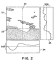
- Figures 2 - 5 are respectively a sketch of an enlarged plan view of the surface of an ITO film produced through a prescribed sputtering process and corresponding two sectional views each showing a surface unevenness distribution taken along indicated dotted lines in atomic force microscope (AFM) analysis; wherein Figures 2 and 4 includes the sketched surface area of 500x500 ⁇ , Figures 3 and 5 include the sketched surface area of 5000x5000 ⁇ , the ITO films as to Figures 2 and 3 are produced through A process appearing hereinafter, and the ITO films as to Figures 4 and 5 are produced through B process appearing hereinafter.
- AFM atomic force microscope
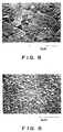
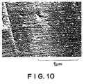
- Figures 6, 8 and 10 are respectively a photomicrograph (x50,000) of an ITO film produced through A process ( Figure 6), B process ( Figure 8) or C process ( Figure 10).
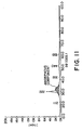
- Figures 7, 9 and 11 are respectively an X-ray diffraction profile (chart) of an ITO film produced through A process ( Figure 7), B process ( Figure 9) or C process ( Figure 11).
- Figure 12 is an X-ray diffraction profile (chart) of a standard silicon (Si) powder as a reference substance for evaluation of crystallinity.
- Figure 13 is a schematic sectional view of an embodiment of a liquid crystal device used in the present invention.
- Figures 14A - 14E are schematic sectional views for illustrating a process for producing a liquid crystal device according to the present invention.
- Figure 15 is a schematic view of an embodiment of a liquid crystal device produced through a conventional production process.
- the display device is characterized by using an electroconductive transparent film (hereinbelow, simply referred to as "transparent film”) having a surface unevenness of at most 30 ⁇ , thus remarkably improving its surface smoothness.
- transparent film an electroconductive transparent film having a surface unevenness of at most 30 ⁇ , thus remarkably improving its surface smoothness.
- surface unevenness means a maximum difference in height (or a difference in height between the highest point and the lowest point) with respect to a horizontal length of 200 - 500 ⁇ (reference length) as measured though an atomic force microscope (AFM) and a scanning tunnel microscope (STM).
- AFM atomic force microscope
- STM scanning tunnel microscope
- a transparent film in order to obviate an uneven surface due to a crystal of a large particle size, a transparent film may be prepare by forming a thin film of a material comprising indium oxide and/or tin oxide, preferably ITO, containing an amorphous component to improve a surface smoothness and provide a decreased surface unevenness (at most 30 ⁇ due to a small particle size at the surface of a resultant film, followed by annealing of the film under suitable conditions (e.g., a temperature of 180 °C or below).
- suitable conditions e.g., a temperature of 180 °C or below.
- the thus prepared transparent film shows a transmittance and a sheet resistance at an acceptable level even when compared with a conventional ITO film having a high crystallinity, and also is excellent in surface flatness, thus sufficiently contributing to an improvement in characteristics of a display device as a display electrode.
- the transparent film retains therein an amorphous component after film formation and accordingly allows a variety of etchants inclusive of weak acids in an etching step during a pattern formation in contract with the conventional high-crystalline ITO film. As a result, damage to underlying layers of the transparent film can be alleviated to enhance performances of a resultant display device provided with the transparent film as a display electrode.
- the transparent film comprising indium oxide and/or tin oxide, particularly ITO film can be formed by using various film-forming processes and conditions.
- an ITO film having a high amorphous degree can be obtained by setting a low power density condition and a low substrate temperature (preferably 100 °C or below).
- a low substrate temperature preferably 100 °C or below.
- an amount of oxygen gas so as to become smaller than a theoretical amount for an ordinary (high-crystalline) ITO film, it is possible to promote an increase of an amorphous component to provide an ITO film surface in fine-particle shape, thus resulting in an excellent surface flatness (e.g., surface uneveness of at most 30 ⁇ ).
- the thus prepared transparent film containing the amorphous component can be accompanied with difficulties, such as a lowered transmittance and a high sheet resistance in some cases.
- film-forming conditions for the transparent film containing an amorphous component and an anneal-treating condition, particularly temperature may preferably be set at low temperature, e.g., at 150 - 300 °C, more preferably at most 200 °C, further preferably at most 180 °C, thus retaining a transmittance and a sheet resistance of a resultant film at a practically acceptable level comparable to that of the high-crystalline ITO film.
- the temperature of heating may preferably at most 280 °C, more preferably at most 250 °C.
- the annealing treatment may preferably be performed after the transparent (ITO) film containing the amorphous component is subjected to patterning by using an etchant, e.g., weak acid, less affecting the lower layers disposed thereunder, in view of realization of an accuracy of patterning and optical and electrical characteristics of the transparent film at the same time.
- an etchant e.g., weak acid
- JP-A 5-151827 described above discloses an amorphous state of ITO and a heat treatment (annealing) thereof.
- a resultant ITO film is formed in order to improve an adhesiveness to a metal film by providing the surface of the ITO film with an unevenness and has a crystal particle size of at least 400 ⁇ as measured according to X-ray diffraction analysis.
- a surface unevenness of the ITO film after the annealing is not concerned with the particle size based on X-ray diffraction.
- the ITO film after the annealing used in the present invention has a decreased surface unevenness (at most 30 ⁇ ), thus being excellent in flatness when compared with the surface-roughened ITO film of JP-A 5-151827.
- the above-described display device using the transparent film as a display electrode according to the present invention is applicable to many display devices of non-light emission type, such as liquid crystal displays and of light emission type, such as electroluminescence display (ELD) and plasma display panel (PDP).
- the transparent film used therein is excellent in surface smoothness while retaining a high transmittance and a low resistance, thus remarkably improving a display performance.
- the display device of the present invention may preferably be used as a liquid crystal (display) device wherein a liquid crystal is sandwiched between a pair of substrates provided with display electrodes and an alignment state of the liquid crystal is controlled by applying a prescribed voltage to the liquid crystal thereby to form a desired display image. More specifically, in such a liquid crystal device, an alignment state of liquid crystal molecules at each pixel is controlled to regulate a light transmittance in accordance with a two-valued scheme or a multi-valued scheme, thus obtaining a desired image.
- an addressing scheme of pixels may be a multiplexing-addressed scheme using an electrode matrix or a light-addressed scheme using a photoconductive film.
- the liquid crystal used in the present invention may be a nematic liquid crystal or a smectic liquid crystal, preferably a liquid crystal assuming a chiral smectic phase and ferroelectricity in view of facility of alignment control.
- a uniformity of properties of an alignment control film is effectively improved due to a good performance, particularly an improved surface flatness of a transparent film (transparent electrode).
- the display device of the present invention may be used as a liquid crystal device of an active matrix-type using a nematic liquid crystal wherein each pixel is provided with a switching element (e.g., a thin film transistor (TFT) or a metal insulator metal (MIM)).
- a switching element e.g., a thin film transistor (TFT) or a metal insulator metal (MIM)
- Figure 1 is a schematic sectional view of an embodiment of the liquid crystal device including a liquid crystal layer for explanation of the structure thereof.
- the liquid crystal device includes a liquid crystal layer 1 disposed between a pair of substrates 2 (e.g., glass substrates) each having thereon a transparent electrode 3 and an alignment control layer 4.
- the substrates 2 are placed or arranged opposite to each other. Outside the substrates 2 a pair of polarizers 8 are disposed so as to modulate incident light I 0 from a light source 9 in cooperation with the liquid crystal 1 to provide modulated light I.
- Each of two glass substrate 2 is coated with a transparent electrode 3 comprising a film, a material comprising indium oxide and/or tin oxide, preferably an ITO film, via at least one layer, as desired, to form an electrode plate.
- the transparent electrode is subjected to patterning so as to provide a prescribed shape corresponding to a pixel shape.
- an alignment control layer 4 having an aligning state control ability of liquid crystal molecules is formed.
- At least one of the alignment control layers 4 may preferably be formed by rubbing a film of a polymer such as polyimide with gauze or acetate fiber-planted cloth so as to uniaixally aligning the liquid crystal molecules in one direction.
- Examples of a material for the alignment control layer may include an inorganic material, such as silicon nitride, silicon carbide containing hydrogen, silicon oxide, boron nitride, boron nitride containing hydrogen, cerium oxide, aluminum oxide, zirconium oxide, titanium oxide, or magnesium fluoride; an organic insulating material, such as polyvinyl alcohol, polyimide, polyamide-imide, polyester-imide, polyparaxylylene, polyester, polycarbonate, polyvinyl acetal, polyvinyl chloride, polyvinyl acetate, polyamide, polystyrene, cellulose resin, melamine resin urea resin, acrylic resin, or photoresist resin.
- an inorganic material such as silicon nitride, silicon carbide containing hydrogen, silicon oxide, boron nitride, boron nitride containing hydrogen, cerium oxide, aluminum oxide, zirconium oxide, titanium oxide, or magnesium fluoride
- the alignment control layer 4 may be formed in two layers each comprising the inorganic and/or organic insulating materials described above. Alternatively, it is also possible to use a single layer of inorganic alignment control layer comprising the above-mentioned inorganic material or organic alignment control layer comprising the above-mentioned organic material.
- An organic alignment control layer may be formed by vapor deposition, while an organic alignment control layer may be formed by applying a solution of an organic insulating material or a precursor thereof in a concentration of 0.1 to 20 wt. %, preferably 0.2 - 10 wt. %, by spinner coating, dip coating, screen printing, spray coating or roller coating, followed by curing or hardening (e.g., by heating) under prescribed hardening conditions.
- the alignment control layer 4 may have a thickness of ordinarily 10 ⁇ - 1 ⁇ m, preferably 10 - 3000 ⁇ , further preferably 10 - 1000 ⁇ .
- the two glass substrates 2 with transparent electrodes 3 and alignment control layers 4 thereof are held to have a prescribed (but arbitrary) gap with a spacer (not shown).
- a spacer (not shown).
- such a cell structure with a prescribed gap may be formed by sandwiching spacers of silica beads or alumina beads having a prescribed diameter with two glass plates, and then sealing the periphery thereof with, a sealing material 5 comprising, e.g., an epoxy adhesive.
- a polymer film or glass fiber may also be used as a spacer.
- a liquid crystal (preferably assuming a chiral smectic phase or ferroelectricity is sealed up to provide a liquid crystal layer 1 in a thickness of generally 0.5 to 20 ⁇ m, preferably 0.5 to 5 ⁇ m.
- the liquid crystal may be a nematic liquid crystal or other smectic liquid crystals.
- the transparent electrodes 3 are connected to the external power supply (not shown) through lead wires (not shown). Further, outside the substrates 2, polarizers 8 are applied.
- the device shown in Figure 1 is used as a transmission-type liquid crystal device by employing transparent substrates (e.g., glass plates) and is provided with a light source 9.
- the above-mentioned liquid crystal device may be modified into a color liquid crystal device, e.g., by forming on at least one substrate a color filter layer (uneven layer) comprising color filter segments of, e.g., red (R), green (G), blue (B) and optional white (transparent) (W) and a flattening layer covering the color filter layer in succession.
- the color filter layer may preferably be formed below the transparent electrodes (i.e., close to the substrate).
- the transparent electrode comprising the transparent film excellent in surface flatness (surface unevenness of at most 30 ⁇ ) is also effective in suppression the influence of the uneven color filter layer together with the flattening layer, thus improving an alignment state of liquid crystal molecules.
- liquid crystal device it is possible to provide to one substrate a switching element (preferably a TFT) connected with a transparent electrode corresponding to pixels.
- a switching element preferably a TFT
- Figure 13 is a schematic sectional view of a substrate structure including a color filter layer used in a color liquid crystal device as an embodiment of the display device of the present invention.
- a black light-interrupting layer (black matrix) 22 and a color filter layer 23 are successively formed on a glass substrate 1 (one of a pair of glass substrate between which a liquid crystal is disposed). Further thereon, a flattening layer 24 and a transparent electrode (ITO film) 27 are disposed in succession.
- the color filter 23 comprises color pixels of red (R), green (G), blue (B) and white (W) and is actuated to effect color display according to additive process by controlled voltage application to the liquid crystal layer between the substrates.
- the flattening layer 24 is formed so as to cover the color filter layer 23 to ensure protection and evenness (smoothness) of the color filter layer 23.
- the transparent electrode 27 comprising a transparent film consisting essentially of indium oxide and/or tin oxide, preferably ITO, contains an amorphous component as described above and patterned in a desired form on the flattening layer 24. On the transparent electrode 27, an insulating layer (not shown) and an alignment control layer (not shown) are successively formed to provide a treated substrate.
- the other treated substrate is prepared in a similar manner except for omitting the light-interrupting layer 22, the color filter layer 23 and the flattening layer 24. These two treated substrates are applied to each other with a spacing, which is then filled with a chiral smectic liquid crystal assuming ferroelectricity (not shown) to prepare a liquid crystal device capable of effecting color display.
- the transparent film (preferably as a display electrode) is formed as a film of a material comprising indium oxide and/or tin oxide, whereby a weak acid-type etchant, such as hydroiodic acid or oxalic acid, can be used in an etching step through a photolithographic process at the time of effecting patterning of the transparent film in a display electrode form.
- a weak acid-type etchant such as hydroiodic acid or oxalic acid
- liquid crystal device particularly a color liquid crystal device wherein a liquid crystal is sandwiched between a pair of oppositely disposed substrates at least one of which is provided with an electrode, and at least one substrate is provided with a color filter layer and a flattening layer covering the color filter layer; a transparent film comprising an indium oxide and/or tin oxide (mixture) film, preferably an ITO film, is formed on the flattening layer and then is coated with a photoresist, followed by etching with a weak acid for providing a desired electrode pattern by using a lithographic process.
- a transparent film comprising an indium oxide and/or tin oxide (mixture) film, preferably an ITO film
- the ITO film may preferably be a film having a low crystallinity satisfying the following relationship: (1/d) x (H1/H2) ⁇ 1/5, wherein d denotes a thickness ( ⁇ m) of the ITO film, H1 denotes a peak intensity at crystal plane (2, 2, 2) of the ITO film according to X-ray diffraction analysis and H2 denotes a peak intensity at crystal plane (1, 1, 1) of a standard (reference) silicon (Si) powder according to X-ray diffraction analysis.
- the ITO film containing an amorphous component increases its amorphous degree when the peak intensity H1 at crystal plane (2, 2, 2) is lowered.
- the peak intensity H1 varies depending on an analysis sensitivity and a thickness of a sample (ITO) film.
- the crystallinity (or amorphous degree) is standardized by using the peak intensity H2 at crystal plane (1, 1, 1) of the standard Si powder and the ITO film thickness d, thus providing the above relationship ((1/d) x (H1/H2) ⁇ 1/5).
- the value of 1/5 corresponds to an upper limit value allowing a good weak-acid etching not causing occurrence of an etching residue.
- a sample ITO film is formed on a glass substrate or a silicon substrate (silicon wafer) and cut to provide a measurement sample having a size of 35 mm x 50 mm.
- the thus prepared measurement sample is subjected to X-ray diffraction analysis by using an X-ray diffraction apparatus ("MXP18", manufactured by MAC Co.) under the following conditions.
- oblique (inclined) observation is effected by using a scanning electron microscope (SEM) ("Model S4100", mfd. by Hitachi Seisakusho K.K.) under the condition of an inclination angle of 45 degrees and an acceleration voltage of 10 - 30 kV.
- SEM scanning electron microscope
- AFM atomic force microscope
- the sample ITO film is formed on a silicon wafer which has been polished with high accuracy. This is because a glass substrate has an undulation component at its surface and accordingly is liable to invite a measurement error in the case of a longer measuring range.
- scanning with the AFM is performed in an area (6000 ⁇ x 6000 ⁇ ) surrounding the indicated region 31 or 51 (5000 ⁇ x 5000 ⁇ ) in such a manner that a horizontal scanning is performed with respect to 256 points along a reference line 32 (or 52) in a horizontal length of 6000 ⁇ while keeping a contact spacing between adjacent measurement points and a vertical scanning is performed similarly as in the horizontal scanning along a reference line 33 (or 53) to provide sectional shapes 34 and 35 (or 54 and 55) of the surface of an objective film. Based on these sectional shapes, a surface unevenness is determined.
- a comparative (high-crystalline) ITO film having a thickness of 800 ⁇ was formed on an objective substrate through an A process (conventional process) under conditions described below, and an 800 ⁇ -thick ITO film was formed on an objective substrate through a B process including a heat treatment under conditions described below.
- the A process is a conventional process for providing a minimum sheet resistance to a resultant ITO film by setting a substrate temperature at 200 °C or above and appropriately controlling a mixing ratio of oxygen gas (O 2 )/argon gas (Ar).
- the B process is process for providing an ITO film containing an amorphous component by controlling a substrate temperature, e.g., at 100 °C or below.
- the mixing ratio of O 2 /Ar is charged under the influence of several factors, such as a vacuum degree and a vacuum quality within a sputtering apparatus, an oxygen content in a target, moisture, and a sputtering power density, and cannot be specified as a certain value.
- the processes (A and B processes) were performed by using a sputtering apparatus ("ILC-705", mfd. by Niommen Anelva K.K.) under the following conditions, respectively.
- Condition A process B process Target ITO* 1 ITO* 1 Substrate temp. (°C) 220 60 Sputtering pressure (mTorr) 3 2 O 2 flow (sccm) 3 2 Ar flow (sccm) 200 200 Conveyance speed (mm/min) 300 300 Sputtering powder (kW) 0.75 0.75 *1:
- a high-density ITO target (density: 95 %, indium oxide: 90 wt. %, tin oxide: 10 wt. %, mfd. by Mitsui Kinzoku K.K.) was used.
- reference numerals 21, 31, 41 and 51 respectively represent a surface state of an associated ITO film.
- Reference numerals 24, 34, 44 and 54 respectively represent a sectional shape of the ITO film taken along dotted lines 22, 32, 42 and 52, respectively, and reference numerals 25, 35, 45 and 55 respectively represents a sectional shape of the ITO film taken along dotted lines 23, 33, 43 and 53, respectively.
- These Figures 2 - 5 are respectively an accurate sketch though image processing by using the AFM and in the (sectional) views of the sectional shapes (24, 25, 34, 35, 44, 45, 54 and 55), a difference in height is appropriately scaled up.
- a bright (or white) portion represents a projection portion and a dark portion represents a recess portion on the basis of a reference line (dotted lines in respective sectional views).
- the ITO film by the B process ( Figure 8) was found to be suppressed in an increase in crystal size and a surface roughening accompanied thereby and to provide a surface flatter (smoother) than the ITO film by the A process ( Figure 6).
- the ITO film by the B process was found to contain an amorphous component (hatched portion) as identified by a shoulder (hollow peak) having an X-ray intensity of ca. 1000 - 2000 cps.
- the ITO film containing an amorphous component produced through the B process was effective in improving a surface flatness.
- this ITO film (B process) was subjected to the annealing (200 °C, 1 hour), the sheet resistance was changed from 120 ohm/cm 2 (before annealing) to 40 ohm/cm 2 and the transmittance (500 nm) was also changed from 80 % (before annealing) to 89 %.
- a resultant liquid crystal device using the ITO film (by the B process) as excellent in surface flatness and provided a low resistance and a high transmittance through the annealing treatment.
- the ITO film (B process) showed an etching time being about 1/5 of that of the ITO film (A process).
- the ITO film (B process) allowed an acid concentration being about 1/2 of that of the etchant for the ITO film (A process) when an identical etching time was set.
- an ITO film was formed through the A process. Further thereon, a 10 nm-thick polyimide alignment control layer was formed by using a polyimide precursor ("LQ-1800", mfd. by Hitachi Kasei K.K.), followed by rubbing with a nylon fiber-planted cloth. The thus prepared two substrates were applied to each other via spacer beads to provide a blank cell, which was then filled with a ferroelectric liquid crystal "ZLI4525", mfd. by Merck Co.), followed by sealing to prepare a liquid crystal cell (device) A1. In a similar manner except for changing the A process to the B process, a liquid crystal cell B1 was prepared-.
- liquid crystal cells A1 and B1 were respectively subjected to voltage application between oppositely disposed transparent electrodes to cause switching of two stable states of the ferroelectric liquid crystal and were subjected to observation of a microscopic uniformity (homogeneity) of an alignment state, whereby the liquid crystal cell A1 showed many alignment defects (due to deviation of layer normal of smectic layers), whereas the liquid crystal cell B1 showed substantially no alignment defects of a problematic level.
- An 800 ⁇ -thick ITO film was formed on an objective substrate though a C process by using a sputtering apparatus ("ILC-3944", mfd. by Niommen Anelva K.K.) under the following conditions.
- Target ITO* 1 Substrate temp. (°C) 25 Sputtering pressure (mTorr) 2.8 O 2 flow (sccm) 0.5 Ar flow (sccm) 140 Conveyance speed (mm/min) 220 Sputtering powder (kW) 1.2 *1: A high-density ITO target (density: 95 %, indium oxide: 90 wt. %, tin oxide: 10 wt. %, mfd. by Mitsui Kinzoku K.K.) was used.
- the ITO film produced by the C process was found to provide a flattened surface.
- Three liquid crystal devices A, B and C were respectively prepared by using a pairs of substrates provided with ITO films produced through the processes A, B and C (for divides A, B and C respectively), in the following manner.
- a 50 ⁇ -thick polyimide alignment control film obtained from a polyimide precursor ("LQ1800", mfd. by Hitachi Kasei K.K.) was formed and rubbed with a nylon fiber-planted cloth.
- the thus prepared two substrates were applied to each other via spacer beads to prepare a blank cell, which was then filled with a ferroelectric liquid crystal containing an optically active compound having a fluorinated chiral portion, followed by sealing to provide an objective liquid crystal cell (device).
- One substrate having plural layers thereon was prepared using the C process adopted in Experiment 2 and forming the indicated layers (structural members) shown below on a glass substrate in the following manner.
- the other substrate was prepared in the same manner as in the above substrate except for omitting the color filter layer and the polymeric flattering layer.
- a liquid crystal device (“panel 2") was prepared by using 800 ⁇ -thick ITO films produced through the B process (used in Experiment 1).
- the panel 2 was found to provide fewer alignment defects than the panel 1.
- the ITO film after produced through the C process rich in etching performance was subjected to patterning by a photographic process, followed by annealing at 200 °C for 1 hour to increase its transmittance (500 nm) of from 82 % to 89 % and decrease its sheet resistance of from 90 ohm/cm 2 to 30 ohm/cm 2 , thus resulting in a suitable transparent electrode.
- a value of a peak intensity of standard Si powder in X-ray diffraction analysis is adopted as a reference peak intensity (H2) in the present invention in order to provide evaluation of the crystallinity with universality.
- Figure 12 is an X-ray diffraction profile of the standard Si powder showing a peak intensity of about 55000 cps at a 2 ⁇ angle of about 30 degrees (for crystal plane (1, 1, 1)).
- a crystal component of an ITO film generally shows a peak intensity of about 17000 to about 17500 at crystal plane (2, 2, 2) as shown in Figure 7 (A process).
- the ITO film containing an amorphous component prepared by the C process provided a peak intensity of about at most 5500 cps (representing crystal peak intensity) including a hollow (shoulder) peak intensity of about 1000 - 2000 cps (representing amorphous component) as shown in Figure 11.
- the ITO crystal peak intensity is increased in proportion to an increase in thickness (of ITO film) up to about 1000 nm and is saturated when the thickness of the ITO film exceeds about 1000 nm.
- the thickness of the ITO films were below 100 nm.
- a 1.1 mm-thick glass substrate 1 was coated with a 1000 ⁇ -thick metal (Mo) film by sputtering and subjected to patterning by a photolithographic process to form a light-interrupting layer (black matrix) 22. Further thereon, photosensitive colored resin were applied and subjected to patterning by a photolithographic process to form a ca. 1.5 ⁇ m-thick color filter layer 23 comprising color pixel segments of red (R), green (G), blue (B) and white (W), respectively.
- Mo metal
- a ca. 1.5 ⁇ m-thick flattening layer 24 comprising polyvinylsiloxane was formed by spin coating ( Figure 14B).
- a ca. 2 ⁇ m-thick photoresist pattern 26 was formed by applying thereon a photoresist and effecting a photolithographic process including an exposure step and a development step ( Figure 14D).
- the ITO film 25 having thereon the photoresist pattern 26 was etched with a weak acid-type etchant, followed by removal of the resist pattern 26 to form a patterned ITO film (transparent electrode) 27 ( Figure 14E).
- the dilution-ratio may preferably be 60:40 to 10:90.
- the thus determined pH value may preferably be above -1.1, more preferably above -1.0.
- the etchant further showed an etching rate of 5 ⁇ /sec (which may more preferably be in a range of 10 - 30 ⁇ /sec) at a liquid temperature of 25 °C and did not contain chlorine ion and bromine ion being liable to pass through the resinous flattening layer 24.
- the etching of the ITO film 25 was performed for a prescribed time being long two times a suitable etching time, i.e., over-etching was performed.
- the ITO film 25 merely showed an amount of etching at sides thereof (side etching amount) of about at most 1 ⁇ m based on a spacing between adjacent pixels (photoresist portions) of about 10 ⁇ m.
- the side etching amount is determined as follows. When an etching is effected by using a photoresist having a pattern with a spacing between adjacent photoresist portions of about 10 ⁇ m (corr. to a pixel spacing), corresponding adjacent ITO film portions after the etching provide a spacing therebetween of about at most 11 ⁇ m. At this time, the side etching amount is about at most 1 ⁇ m.
- an insulating film (not shown) an an alignment control film (not shown) are successively formed to provide one treated substrate.
- the other treated substrate is prepared in the same manner as in the above treated substrate except that the color filter layer 23 and the flattening layer 24 are not formed.
- a liquid crystal e.g., a nematic liquid crystal, a smectic liquid crystal, a chiral smectic liquid crystal, particularly a ferroelectric liquid crystal, etc.
- properties of the patterned ITO film 27 can be improved by heat treatment including annealing in the steps of the device production process subsequent to the patterning step thereof, e.g., by heat treatment in the step of forming an alignment control film.
- the ITO film 25 containing an amorphous component could be formed by decreasing the substrate temperature, the sputtering pressure (high vacuum state) and the O 2 flow.
- the appropriately diluted hydroiodic acid as an etchant, it was possible to suppress a reaction with a trace metal component contained in the flattening layer 24, thus preventing occurrences of peeling of the flattening layer 24 and a microcrack therein.
- the ITO film 25 containing an amorphous component has a surface smoother than the high-crystalline ITO film, thus being excellent in surface evenness and not adversely affecting a flatness of an upper alignment control layer controlling an alignment state of liquid crystal molecules. As a result, a resultant liquid crystal device (as a final product) is excellent in liquid crystal-aligning control performance.
- a 1000 ⁇ -thick black matrix 22, a ca. 1.5 ⁇ m-thick color filter layer 23 and a ca. 1.5 ⁇ m-thick flattening layer were successively formed on a 1.1 mm-thick glass substrate 1 in the same manner as in Example 2 ( Figures 14A and 14B).
- the thus prepared ITO film was subjected to X-ray diffraction analysis, whereby it was found to satisfy the relationship: (1/d) x (H1/H2) ⁇ 1/5, thus confirming a low crystallinity.
- a ca. 2 ⁇ m-thick photoresist pattern 26 was formed by applying thereon a photoresist and effecting a photolithographic process including an exposure step and a development step ( Figure 14D).
- the ITO film 25 having thereon the photoresist pattern 26 was etched with a weak acid-type etchant, followed by removal of the resist pattern 26 to form a patterned ITO film (transparent electrode) 27 ( Figure 14E).
- the resultant (patterned) ITO film prepared in this example showed a side etching amount of at most 1 ⁇ m and did not cause occurrences of peeling of the flattening layer 24 and microcracks therein because of the use of the appropriately diluted hydroiodic acid (etchant).
- the use of the appropriately diluted hydroiodic acid contributed to cost saving of production costs of the device since available hydroiodic acid was expensive.
- a color liquid crystal device was prepared by using the above-patterned iTO film 27 otherwise in the same manner as in Example 2.
- the patterned ITO film 27 may preferably be subjected to appropriate annealing, as desired.
- a transparent film comprising a material comprising indium oxide - tin oxide, particularly an ITO film as a display electrode, it is possible to attain a surface flatness and maintain a transmittance and a sheet resistance through annealing, as desired, thus realizing a display device exhibiting excellent display characteristics.
- patterning of an ITO film containing an amorphous component formed on a substrate constituting a display device can be performed by applying thereto a photoresist and subjecting it to etching with a weak acid-type etchant, so that the weak acid-type etchant does not adversely affects (damages) its underlying layers, such as a flattening layer and a color filter layer in the case of a color liquid crystal device.
- a weak acid-type etchant does not adversely affects (damages) its underlying layers, such as a flattening layer and a color filter layer in the case of a color liquid crystal device.
Landscapes
- Physics & Mathematics (AREA)
- Nonlinear Science (AREA)
- Mathematical Physics (AREA)
- Chemical & Material Sciences (AREA)
- Crystallography & Structural Chemistry (AREA)
- General Physics & Mathematics (AREA)
- Optics & Photonics (AREA)
- Liquid Crystal (AREA)
- Non-Insulated Conductors (AREA)
- Devices For Indicating Variable Information By Combining Individual Elements (AREA)
Applications Claiming Priority (4)
| Application Number | Priority Date | Filing Date | Title |
|---|---|---|---|
| JP7353474A JPH09185062A (ja) | 1995-12-27 | 1995-12-27 | 表示素子 |
| JP353474/95 | 1995-12-27 | ||
| JP7344057A JPH09185045A (ja) | 1995-12-28 | 1995-12-28 | 液晶素子の製造方法 |
| JP344057/95 | 1995-12-28 |
Publications (2)
| Publication Number | Publication Date |
|---|---|
| EP0782039A2 true EP0782039A2 (fr) | 1997-07-02 |
| EP0782039A3 EP0782039A3 (fr) | 1998-06-17 |
Family
ID=26577681
Family Applications (1)
| Application Number | Title | Priority Date | Filing Date |
|---|---|---|---|
| EP96309541A Withdrawn EP0782039A3 (fr) | 1995-12-27 | 1996-12-24 | Dispositif d'affichage et son procédé de fabrication |
Country Status (2)
| Country | Link |
|---|---|
| US (1) | US6310674B1 (fr) |
| EP (1) | EP0782039A3 (fr) |
Cited By (2)
| Publication number | Priority date | Publication date | Assignee | Title |
|---|---|---|---|---|
| EP1168376A4 (fr) * | 1998-12-10 | 2007-05-02 | Au Optronics Corp | Procede de formation d'un film conducteur transparent a l'aide d'une reserve amplifiee chimiquement |
| US8054397B2 (en) | 2003-03-25 | 2011-11-08 | Semiconductor Energy Laboratory Co., Ltd. | Display device and manufacturing method thereof |
Families Citing this family (14)
| Publication number | Priority date | Publication date | Assignee | Title |
|---|---|---|---|---|
| KR20050061610A (ko) * | 1999-06-11 | 2005-06-22 | 마쯔시다덴기산교 가부시키가이샤 | 액정표시장치 |
| WO2002007171A1 (fr) * | 2000-07-19 | 2002-01-24 | Matsushita Electric Industrial Co., Ltd. | Substrat auquel est attachee une electrode et procede de preparation associe |
| JP2002072257A (ja) * | 2000-09-05 | 2002-03-12 | Fuji Xerox Co Ltd | 表示素子 |
| FR2817977B1 (fr) * | 2000-12-12 | 2003-03-07 | Nemoptic | Procede de realisation d'un dispositif a cristaux liquides perfectionne, et dispositif ainsi obtenu |
| KR100778835B1 (ko) * | 2000-12-28 | 2007-11-22 | 엘지.필립스 엘시디 주식회사 | 액정표시장치의 제조방법 |
| JP2002296609A (ja) * | 2001-03-29 | 2002-10-09 | Nec Corp | 液晶表示装置及びその製造方法 |
| TWI245958B (en) * | 2001-05-11 | 2005-12-21 | Matsushita Electric Industrial Co Ltd | Liquid crystal display panel and process for producing same |
| FR2840694B1 (fr) * | 2002-06-06 | 2004-08-27 | Nemoptic | Procede de realisation de dispositifs a cristaux liquides nematiques |
| TW588184B (en) * | 2002-07-30 | 2004-05-21 | Hong-Da Liu | Ultra minimal roughness reflective layer for pixel designed thin film transistor and liquid crystal display |
| CN100437251C (zh) * | 2002-08-16 | 2008-11-26 | Nec液晶技术株式会社 | 在涂覆形成的夹层绝缘膜上具有透明导电膜的液晶显示器 |
| US7497973B2 (en) * | 2005-02-02 | 2009-03-03 | Lumination Llc | Red line emitting phosphor materials for use in LED applications |
| US7372610B2 (en) | 2005-02-23 | 2008-05-13 | Sage Electrochromics, Inc. | Electrochromic devices and methods |
| CN102968200B (zh) * | 2011-09-01 | 2016-08-03 | 宸美(厦门)光电有限公司 | 镜片触控装置及其制程方法 |
| JP6408042B2 (ja) * | 2017-01-24 | 2018-10-17 | 株式会社東芝 | 光電変換素子およびその製造方法 |
Citations (1)
| Publication number | Priority date | Publication date | Assignee | Title |
|---|---|---|---|---|
| JPH0784271A (ja) * | 1993-09-13 | 1995-03-31 | Casio Comput Co Ltd | 反強誘電性液晶表示素子 |
Family Cites Families (17)
| Publication number | Priority date | Publication date | Assignee | Title |
|---|---|---|---|---|
| DE253512C (fr) | ||||
| JPH0762751B2 (ja) * | 1985-10-03 | 1995-07-05 | セイコーエプソン株式会社 | カラ−液晶表示体 |
| US4796980A (en) | 1986-04-02 | 1989-01-10 | Canon Kabushiki Kaisha | Ferroelectric liquid crystal optical modulation device with regions within pixels to initiate nucleation and inversion |
| DD253512B3 (de) * | 1986-10-21 | 1993-02-25 | Werk Fernsehelektronik Gmbh | Verfahren zur herstellung transparenter leitfaehiger metalloxidstrukturen |
| JP2644743B2 (ja) * | 1987-01-28 | 1997-08-25 | 株式会社日立製作所 | 液晶表示装置の製造方法 |
| US5076671A (en) | 1988-12-22 | 1991-12-31 | Canon Kabushiki Kaisha | Liquid crystal device having two bistable orientation states in the chiral smectic temperature range |
| JPH02251990A (ja) * | 1989-03-27 | 1990-10-09 | Ricoh Co Ltd | 透明電極パターンの作成方法 |
| JP3117446B2 (ja) * | 1989-06-15 | 2000-12-11 | 株式会社半導体エネルギー研究所 | 酸化物導電膜の成膜加工方法 |
| US5105291A (en) * | 1989-11-20 | 1992-04-14 | Ricoh Company, Ltd. | Liquid crystal display cell with electrodes of substantially amorphous metal oxide having low resistivity |
| JP2814155B2 (ja) | 1990-08-13 | 1998-10-22 | キヤノン株式会社 | Ito膜パターンの形成方法および液晶表示素子用基板の製造方法 |
| JP2700945B2 (ja) | 1990-08-30 | 1998-01-21 | キヤノン株式会社 | カラーフィルター付き基板 |
| US5327272A (en) * | 1991-03-27 | 1994-07-05 | Canon Kabushiki Kaisha | Optical modulation element |
| JP3100014B2 (ja) | 1991-12-10 | 2000-10-16 | キヤノン株式会社 | 強誘電性液晶素子及び該素子の製造方法 |
| US5467209A (en) | 1992-01-24 | 1995-11-14 | Canon Kabushiki Kaisha | Ferroelectric liquid crystal device with particular layer thicknesses at non-pixel portions and pixel portions |
| JPH0680565B2 (ja) | 1992-04-22 | 1994-10-12 | 旭硝子株式会社 | 導体付き基板 |
| JP3028271B2 (ja) * | 1993-07-09 | 2000-04-04 | キヤノン株式会社 | 液晶表示素子及びその製造方法 |
| JP3143591B2 (ja) * | 1995-09-14 | 2001-03-07 | キヤノン株式会社 | 表示装置 |
-
1996
- 1996-12-24 EP EP96309541A patent/EP0782039A3/fr not_active Withdrawn
- 1996-12-27 US US08/773,897 patent/US6310674B1/en not_active Expired - Fee Related
Patent Citations (1)
| Publication number | Priority date | Publication date | Assignee | Title |
|---|---|---|---|---|
| JPH0784271A (ja) * | 1993-09-13 | 1995-03-31 | Casio Comput Co Ltd | 反強誘電性液晶表示素子 |
Cited By (3)
| Publication number | Priority date | Publication date | Assignee | Title |
|---|---|---|---|---|
| EP1168376A4 (fr) * | 1998-12-10 | 2007-05-02 | Au Optronics Corp | Procede de formation d'un film conducteur transparent a l'aide d'une reserve amplifiee chimiquement |
| US8054397B2 (en) | 2003-03-25 | 2011-11-08 | Semiconductor Energy Laboratory Co., Ltd. | Display device and manufacturing method thereof |
| US8432505B2 (en) | 2003-03-25 | 2013-04-30 | Semiconductor Energy Laboratory Co., Ltd. | Display device and manufacturing method thereof |
Also Published As
| Publication number | Publication date |
|---|---|
| EP0782039A3 (fr) | 1998-06-17 |
| US6310674B1 (en) | 2001-10-30 |
Similar Documents
| Publication | Publication Date | Title |
|---|---|---|
| US6310674B1 (en) | Method of making a display device with electrode characteristics | |
| CN101435961B (zh) | Tft-lcd彩膜/阵列基板、液晶显示面板及其制造方法 | |
| KR100647097B1 (ko) | 액정 표시 장치 및 그 제조 방법 | |
| EP0541388B1 (fr) | Procédé de fabrication d'un dispositif d'affichage à crystal liquide | |
| US6417898B1 (en) | Liquid crystal display device | |
| US4744637A (en) | Liquid crystal device with a protective layer of a particular coefficient of expansion | |
| EP1069462A1 (fr) | Dispositif d'affichage à cristal liquide et son procédé de fabrication | |
| US5815230A (en) | Liquid crystal device and process for production thereof | |
| CN102629025B (zh) | 彩膜基板及其制造方法和液晶显示面板 | |
| EP0788013B1 (fr) | Substrat d'électrodes pour dispositif à cristal liquide et son procédé de fabrication | |
| US5396356A (en) | Color liquid crystal device with non-driving electrodes under the sealant for providing an even cell gap | |
| CN1508598A (zh) | 液晶显示装置的制造方法 | |
| CN1238755C (zh) | 形成液晶显示器件的金属线的方法 | |
| US6930748B2 (en) | Liquid crystal display device and method for manufacturing the same | |
| JP3395884B2 (ja) | 液晶表示パネルおよびその製造方法 | |
| JPH04324938A (ja) | 薄膜トランジスタとその製造方法 | |
| JPH09185062A (ja) | 表示素子 | |
| JPH06331948A (ja) | 液晶電気光学装置作製方法 | |
| CN1584636A (zh) | 彩色滤光片及其制作方法 | |
| WO2022032894A1 (fr) | Matrice noire pour panneau à cristaux liquides et panneau à cristaux liquides | |
| US5499125A (en) | Liquid crystal display with a smoothing film in a treached substrate and method for forming the same | |
| JP2000147507A (ja) | 液晶表示素子及びその製造方法 | |
| JPH07104264A (ja) | 液晶表示装置 | |
| EP0768558B1 (fr) | Dispositif à cristal liquide et procédé pour sa fabrication | |
| JP2983724B2 (ja) | 強誘電性液晶素子の配向処理法 |
Legal Events
| Date | Code | Title | Description |
|---|---|---|---|
| PUAI | Public reference made under article 153(3) epc to a published international application that has entered the european phase |
Free format text: ORIGINAL CODE: 0009012 |
|
| AK | Designated contracting states |
Kind code of ref document: A2 Designated state(s): DE FR GB IT NL |
|
| PUAL | Search report despatched |
Free format text: ORIGINAL CODE: 0009013 |
|
| AK | Designated contracting states |
Kind code of ref document: A3 Designated state(s): DE FR GB IT NL |
|
| 17P | Request for examination filed |
Effective date: 19981029 |
|
| 17Q | First examination report despatched |
Effective date: 19990922 |
|
| GRAP | Despatch of communication of intention to grant a patent |
Free format text: ORIGINAL CODE: EPIDOSNIGR1 |
|
| STAA | Information on the status of an ep patent application or granted ep patent |
Free format text: STATUS: THE APPLICATION IS DEEMED TO BE WITHDRAWN |
|
| 18D | Application deemed to be withdrawn |
Effective date: 20050607 |