EP0782123A1 - Appareil à cristaux liquides et méthode d'attaque pour éviter le phénomène de jaunissement - Google Patents
Appareil à cristaux liquides et méthode d'attaque pour éviter le phénomène de jaunissement Download PDFInfo
- Publication number
- EP0782123A1 EP0782123A1 EP96309468A EP96309468A EP0782123A1 EP 0782123 A1 EP0782123 A1 EP 0782123A1 EP 96309468 A EP96309468 A EP 96309468A EP 96309468 A EP96309468 A EP 96309468A EP 0782123 A1 EP0782123 A1 EP 0782123A1
- Authority
- EP
- European Patent Office
- Prior art keywords
- liquid crystal
- frequency
- denotes
- data signal
- period
- Prior art date
- Legal status (The legal status is an assumption and is not a legal conclusion. Google has not performed a legal analysis and makes no representation as to the accuracy of the status listed.)
- Withdrawn
Links
- 239000004973 liquid crystal related substance Substances 0.000 title claims abstract description 180
- 238000000034 method Methods 0.000 title claims description 16
- 238000004383 yellowing Methods 0.000 title description 5
- 230000008859 change Effects 0.000 claims abstract description 29
- 239000000758 substrate Substances 0.000 claims abstract description 26
- 230000005684 electric field Effects 0.000 claims abstract description 13
- 230000001186 cumulative effect Effects 0.000 claims abstract description 8
- 239000011159 matrix material Substances 0.000 claims abstract description 8
- 239000004990 Smectic liquid crystal Substances 0.000 claims description 29
- 210000004027 cell Anatomy 0.000 description 30
- 210000002858 crystal cell Anatomy 0.000 description 23
- 239000010410 layer Substances 0.000 description 23
- 239000000463 material Substances 0.000 description 8
- 239000000203 mixture Substances 0.000 description 6
- 238000007789 sealing Methods 0.000 description 6
- 238000005259 measurement Methods 0.000 description 5
- VYPSYNLAJGMNEJ-UHFFFAOYSA-N Silicium dioxide Chemical compound O=[Si]=O VYPSYNLAJGMNEJ-UHFFFAOYSA-N 0.000 description 4
- 239000000470 constituent Substances 0.000 description 4
- 230000003247 decreasing effect Effects 0.000 description 4
- 239000005262 ferroelectric liquid crystals (FLCs) Substances 0.000 description 4
- 239000004988 Nematic liquid crystal Substances 0.000 description 3
- CZPWVGJYEJSRLH-UHFFFAOYSA-N Pyrimidine Chemical compound C1=CN=CN=C1 CZPWVGJYEJSRLH-UHFFFAOYSA-N 0.000 description 3
- 239000011324 bead Substances 0.000 description 3
- 230000000694 effects Effects 0.000 description 3
- 230000010287 polarization Effects 0.000 description 3
- 230000004043 responsiveness Effects 0.000 description 3
- 238000012360 testing method Methods 0.000 description 3
- 230000007704 transition Effects 0.000 description 3
- POAOYUHQDCAZBD-UHFFFAOYSA-N 2-butoxyethanol Chemical compound CCCCOCCO POAOYUHQDCAZBD-UHFFFAOYSA-N 0.000 description 2
- SECXISVLQFMRJM-UHFFFAOYSA-N N-Methylpyrrolidone Chemical compound CN1CCCC1=O SECXISVLQFMRJM-UHFFFAOYSA-N 0.000 description 2
- 239000004677 Nylon Substances 0.000 description 2
- 239000003795 chemical substances by application Substances 0.000 description 2
- 238000005520 cutting process Methods 0.000 description 2
- 238000011156 evaluation Methods 0.000 description 2
- 239000010419 fine particle Substances 0.000 description 2
- 229920001778 nylon Polymers 0.000 description 2
- 238000012545 processing Methods 0.000 description 2
- 239000000377 silicon dioxide Substances 0.000 description 2
- 230000002269 spontaneous effect Effects 0.000 description 2
- 238000004544 sputter deposition Methods 0.000 description 2
- OXPDQFOKSZYEMJ-UHFFFAOYSA-N 2-phenylpyrimidine Chemical compound C1=CC=CC=C1C1=NC=CC=N1 OXPDQFOKSZYEMJ-UHFFFAOYSA-N 0.000 description 1
- YCKRFDGAMUMZLT-UHFFFAOYSA-N Fluorine atom Chemical compound [F] YCKRFDGAMUMZLT-UHFFFAOYSA-N 0.000 description 1
- 239000004952 Polyamide Substances 0.000 description 1
- 239000004642 Polyimide Substances 0.000 description 1
- 229910003070 TaOx Inorganic materials 0.000 description 1
- 239000002253 acid Substances 0.000 description 1
- 239000000853 adhesive Substances 0.000 description 1
- 230000001070 adhesive effect Effects 0.000 description 1
- 230000015572 biosynthetic process Effects 0.000 description 1
- 230000003098 cholesteric effect Effects 0.000 description 1
- 239000011248 coating agent Substances 0.000 description 1
- 238000000576 coating method Methods 0.000 description 1
- 238000004891 communication Methods 0.000 description 1
- 239000002131 composite material Substances 0.000 description 1
- 150000001875 compounds Chemical class 0.000 description 1
- 238000007796 conventional method Methods 0.000 description 1
- 239000013078 crystal Substances 0.000 description 1
- 238000013500 data storage Methods 0.000 description 1
- 238000009792 diffusion process Methods 0.000 description 1
- 238000009826 distribution Methods 0.000 description 1
- 230000009189 diving Effects 0.000 description 1
- 239000004744 fabric Substances 0.000 description 1
- 229910052731 fluorine Inorganic materials 0.000 description 1
- 239000011737 fluorine Substances 0.000 description 1
- 239000011521 glass Substances 0.000 description 1
- 230000005484 gravity Effects 0.000 description 1
- 230000006872 improvement Effects 0.000 description 1
- 229910003437 indium oxide Inorganic materials 0.000 description 1
- PJXISJQVUVHSOJ-UHFFFAOYSA-N indium(iii) oxide Chemical compound [O-2].[O-2].[O-2].[In+3].[In+3] PJXISJQVUVHSOJ-UHFFFAOYSA-N 0.000 description 1
- AMGQUBHHOARCQH-UHFFFAOYSA-N indium;oxotin Chemical compound [In].[Sn]=O AMGQUBHHOARCQH-UHFFFAOYSA-N 0.000 description 1
- 239000011810 insulating material Substances 0.000 description 1
- 230000003993 interaction Effects 0.000 description 1
- 239000007788 liquid Substances 0.000 description 1
- 238000007726 management method Methods 0.000 description 1
- 230000003287 optical effect Effects 0.000 description 1
- 229920000620 organic polymer Polymers 0.000 description 1
- 230000002093 peripheral effect Effects 0.000 description 1
- 230000000704 physical effect Effects 0.000 description 1
- 229920002647 polyamide Polymers 0.000 description 1
- 229920001721 polyimide Polymers 0.000 description 1
- -1 polysiloxane Polymers 0.000 description 1
- 229920001296 polysiloxane Polymers 0.000 description 1
- 238000003825 pressing Methods 0.000 description 1
- 230000008569 process Effects 0.000 description 1
- 239000002356 single layer Substances 0.000 description 1
- 239000002904 solvent Substances 0.000 description 1
- 125000006850 spacer group Chemical group 0.000 description 1
- 238000001228 spectrum Methods 0.000 description 1
- 238000004528 spin coating Methods 0.000 description 1
- XOLBLPGZBRYERU-UHFFFAOYSA-N tin dioxide Chemical compound O=[Sn]=O XOLBLPGZBRYERU-UHFFFAOYSA-N 0.000 description 1
- 229910001887 tin oxide Inorganic materials 0.000 description 1
- 238000012546 transfer Methods 0.000 description 1
- 238000009281 ultraviolet germicidal irradiation Methods 0.000 description 1
Images


Classifications
-
- G—PHYSICS
- G09—EDUCATION; CRYPTOGRAPHY; DISPLAY; ADVERTISING; SEALS
- G09G—ARRANGEMENTS OR CIRCUITS FOR CONTROL OF INDICATING DEVICES USING STATIC MEANS TO PRESENT VARIABLE INFORMATION
- G09G3/00—Control arrangements or circuits, of interest only in connection with visual indicators other than cathode-ray tubes
- G09G3/20—Control arrangements or circuits, of interest only in connection with visual indicators other than cathode-ray tubes for presentation of an assembly of a number of characters, e.g. a page, by composing the assembly by combination of individual elements arranged in a matrix no fixed position being assigned to or needed to be assigned to the individual characters or partial characters
- G09G3/34—Control arrangements or circuits, of interest only in connection with visual indicators other than cathode-ray tubes for presentation of an assembly of a number of characters, e.g. a page, by composing the assembly by combination of individual elements arranged in a matrix no fixed position being assigned to or needed to be assigned to the individual characters or partial characters by control of light from an independent source
- G09G3/36—Control arrangements or circuits, of interest only in connection with visual indicators other than cathode-ray tubes for presentation of an assembly of a number of characters, e.g. a page, by composing the assembly by combination of individual elements arranged in a matrix no fixed position being assigned to or needed to be assigned to the individual characters or partial characters by control of light from an independent source using liquid crystals
- G09G3/3611—Control of matrices with row and column drivers
- G09G3/3622—Control of matrices with row and column drivers using a passive matrix
- G09G3/3629—Control of matrices with row and column drivers using a passive matrix using liquid crystals having memory effects, e.g. ferroelectric liquid crystals
-
- G—PHYSICS
- G09—EDUCATION; CRYPTOGRAPHY; DISPLAY; ADVERTISING; SEALS
- G09G—ARRANGEMENTS OR CIRCUITS FOR CONTROL OF INDICATING DEVICES USING STATIC MEANS TO PRESENT VARIABLE INFORMATION
- G09G2310/00—Command of the display device
- G09G2310/06—Details of flat display driving waveforms
-
- G—PHYSICS
- G09—EDUCATION; CRYPTOGRAPHY; DISPLAY; ADVERTISING; SEALS
- G09G—ARRANGEMENTS OR CIRCUITS FOR CONTROL OF INDICATING DEVICES USING STATIC MEANS TO PRESENT VARIABLE INFORMATION
- G09G2320/00—Control of display operating conditions
- G09G2320/02—Improving the quality of display appearance
- G09G2320/0247—Flicker reduction other than flicker reduction circuits used for single beam cathode-ray tubes
Definitions
- the present invention relates to a liquid crystal apparatus including a liquid crystal device which may be used as a display device for a television receiver, a view finder for a video camera or a terminal monitor for a computer, or a light valve for a liquid crystal printer, a projector, etc., and a drive method of such a liquid crystal device.
- a liquid crystal device which may be used as a display device for a television receiver, a view finder for a video camera or a terminal monitor for a computer, or a light valve for a liquid crystal printer, a projector, etc., and a drive method of such a liquid crystal device.
- a liquid crystal display device of a passive matrix drive-type using a TN (twisted nematic) liquid crystal has been known as a device which can be produced at a relatively low cost.
- the passive matrix-drive type liquid crystal device using a TN-liquid crystal has a certain limitation due to the occurrence of a crosstalk or a lowering in contrast along with the increase in number of drive lines so that it cannot be said to be suitable as a display device requiring a high resolution and a large number of drive lines, e.g., a liquid crystal television panel.
- a liquid crystal showing a chiral smectic phase such as chiral smectic C (SmC*) phase or chiral smectic H (SmH*) phase
- a chiral smectic phase such as chiral smectic C (SmC*) phase or chiral smectic H (SmH*) phase
- the SSFLCD is one of chiral smectic liquid crystal devices.
- chiral smectic liquid crystal molecules shows a property of assuming either one of two stable states responding to an electric field applied thereto and maintaining such a state in the absence of a sufficient electric field, namely bistability and a memory characteristic, and also has a quick responsiveness to the change in electric field.
- the SSFLCD is expected to be widely used as a display device showing a high-speed responsiveness and a memory characteristic.
- a simple matrix-addressed drive scheme utilizing a memory characteristic is generally used.
- a plurality of scanning electrodes and a plurality of data electrodes are arranged in a matrix from in order to effect a multiplexing drive with respect to a chiral smectic liquid crystal.
- a scanning signal is successively applied to the scanning electrodes in synchronism with application of a data signal to associated data electrodes.
- a data signal determining a display state is applied to data electrodes and a scanning signal designating a writing time (writing period) at a period (time cycle) determined by a duty factor with respect to a data signal pulse used is successively applied to scanning electrodes.
- a display state of each pixel in a selection period is determined in accordance with a combined (composite) signal of the scanning signal and the data signal.
- each of pixels is always subjected to the influence of a change in electric field by a data signal application.
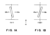
- Liquid crystal molecules minutely vibrate on a cone (a cone-shaped plane on which liquid crystal molecules can be placed) within a degree not causing inversion by the interaction between the constantly varying electric field and a spontaneous polarization of liquid crystal molecules, whereby it has been clarified that a translational movement (uniform motion in one line or direction) of a center of gravity of liquid crystal molecules is induced. More specifically, as shown in Figures 1A and 1B each of liquid crystal molecules assumes either one of two stable state, i.e., a U1 state ( Figure 1A) or U2 state ( Figure 1B).
- the liquid crystal molecule in the U1 state shown in Figure 1A is moved in a direction 12a or a direction 12b and the liquid crystal molecule in the U2 state shown in Figure 1B is moved in a direction 13a or a direction 13b.
- These directions 12a, 12b, 13a and 13b are perpendicular to a direction 11 of a uniaxial aligning treatment (e.g., rubbing) axis.
- the directions 12a and 13a are taken as a positive direction in the U1 state and a positive direction in the U2 state respectively.
- the liquid crystal sandwiched between the substrates is accumulated at a peripheral portion of the device or an end portion of a writing region to increase a cell thickness (a thickness of the liquid crystal layer).
- a retardation (a difference in phase based on birefringence) ⁇ nd is increased thus shifting a wavelength distribution of a transmitted light to a wavelength range assuming yellow (called "yellowing (phenomenon"). Due to this yellowing phenomenon resulting from a change in transmitted light spectrum, a display quality is lowered.
- an effective electric field applied to the liquid crystal is lowered to cause a display unevenness within a display panel.
- a moving direction of a liquid crystal is changed by not only the structural members (factors) but also a liquid crystal material or driving conditions of a liquid crystal device, such as a drive temperature, a drive frequency and a drive voltage.
- a data signal applied to data electrodes is changed in its waveform pattern and frequency corresponding to a display state of a liquid crystal device.
- the liquid crystal movement is induced by a change in electric field of the applied data signal, so that the direction and amount of liquid crystal movement are changed correspondingly by a change of a display state or a display pattern.
- an object of the present invention is to provide a liquid crystal apparatus including a liquid crystal device, particularly a chiral smectic liquid crystal device, in which a liquid crystal movement phenomenon is suppressed or minimized to prevent a yellowing phenomenon leading to a lowering in display quality and to provide a decreased display unevenness.
- Another object of the present invention is to provide a liquid crystal apparatus including a liquid crystal device in which an amount of a liquid crystal movement is suppressed or minimized based on consideration of a relationship between a display pattern and a diving waveform.
- a further object of the present invention is to provide a driving method for the liquid crystal device described above.
- a liquid crystal apparatus comprising:
- a driving method for a liquid crystal device of the type comprising a pair of substrates respectively having thereon scanning electrodes and data electrodes arranged in a matrix shape, and a liquid crystal disposed between the substrates and capable of causing a cumulative translational movement depending on a change in an external electric field applied to the liquid crystal; said driving method comprising: controlling a first frequency f having a variable range and representing an effective frequency of a drive data signal pulse applied to the liquid crystal so that a second frequency f 0 representing an inversion frequency at which a direction of the translational movement of the liquid crystal is turned in an opposite direction is in the variable range of the first frequency f.
- Figures 1A and 1B are schematic views each showing an embodiment of a relationship between one stable state (U1 and U2) and a direction of movement with respect to chiral smectic (ferroelectric) liquid crystal molecules.
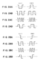
- Figures 2AA - 2AD and Figures 2BA - 2BD are respectively an embodiment of a driving waveform of a data signal in one line writing period (1H) for providing a U1 state or a U2 state.
- FIgure 3 is a schematic sectional view of an embodiment of a liquid crystal device used in the present invention.
- Figures 4A and 4B are respectively a schematic plan view showing an embodiment of a liquid crystal cell for measuring a moving rate of liquid crystal molecules.
- Figure 5 is a schematic plan view showing an embodiment of a liquid crystal movement phenomenon.
- Figure 6 is a graph for illustrating a voltage-dependence of a liquid crystal moving rate and a frequency-dependence of the liquid crystal moving rate.
- Figure 7 is a schematic sectional view of a display pattern for evaluating a cell thickness change in a durability test.
- Figure 8 is a graph for illustrating a change in number of scanning lines with time in a region 74 shown in Figure 7.
- Figure 9 is a graph showing a relationship between a liquid crystal moving rate an a drive data signal frequency in Experimental Example 1 appearing hereinafter.
- the present invention is based on a discovery that the direction of a cumulative translational movement of liquid crystal molecules is turned in an opposite direction at a certain (second) frequency (f 0 ) of a drive data signal pulse (hereinafter, sometimes referred to as "inversion frequency") even if the liquid crystal molecules are placed in any one of two stable states (U1 and U2 states as shown in Figure 1).
- a liquid crystal device used may adopt therein the conventional methods for preventing the liquid crystal movement as described above (e.g., cell gap control, the use of uneven substrate surface, and the use of suitable liquid crystal material).
- a third frequency f 1 yx1/(1H) wherein y denotes a natural number satisfying a relationship of z/2 ⁇ y ⁇ (z+1)/2 where z denotes the number of a change in sign (+ or -) of data signal potential in a 1H period, and 1H denotes a selection period for one-line writing (a time required for one-line writing);
- the third frequency f 1 and the second frequency (inversion frequency) f 0 may preferably satisfy the following relationship: 0.5xf 1 ⁇ f 0 ⁇ 1.5xf 1 .
- This relationship may preferably be adopted in case where the liquid crystal device is driven by a multiplexing driving scheme wherein a drive waveform unit of a data signal in a 1H period being an even-function waveform as shown in Figures 2AA - 2AD and a drive waveform unit of a data signal in a 1H period being an odd-function waveform a shown in Figures 2BA - 2BD are appropriately selected, as desired, in order to minimize a flickering phenomenon.
- the second (inversion) frequency f 0 can be determined by effecting a drive test using an entire liquid crystal device or a part of the liquid crystal device in a manner described hereinafter.
- liquid crystal device is driven by a multiplexing driving scheme wherein a drive waveform unit of a data signal in a 1H period is an even-function waveform as shown in
- the second and third frequencies f 0 and f 1 may preferably satisfy the following relationship: f 1 ⁇ f 0 ⁇ 1.5xf 1 .
- the second and third frequencies f 0 and f 1 may preferably satisfy the following relationship: 0.5xf 1 ⁇ f 0 ⁇ f 1 .
- the even-function waveform means a drive signal waveform having an even-numbered z (z: the number of change in sign of data signal potential in a 1H period as defined above) as shown in Figures 2AA - 2AD and the odd-function waveform means a drive signal waveform having an odd-numbered z as shown in Figures 2BA - 2BD.
- a data signal waveform for providing a U1 state shown in Figure 2A include a change in sign of data signal potential: (+) ⁇ (-) ⁇ (+), thus resulting in the number of sign change being 2 (even number).
- a drive means capable of controlling frequencies of data signal pulse so as to satisfy the relationships between the first and second frequencies (f and f 0 ) and between the second and third frequencies (f 0 and f 1 ) described above, it is possible to provide a liquid crystal apparatus, using a chiral smectic liquid crystal device with a high reliability and a minimized display irregularity accompanied with a cell thickness increase in a panel even if a display pattern is changed.
- the liquid crystal movement is affected by various factors, such as a frequency, a voltage and a bias ratio of a drive waveform but the direction of liquid crystal movement is largely affected by the frequency of the drive waveform used.
- the inversion frequency f 0 is liable to be changed by a cell thickness, a surface shape (e.g., uneven shape) of substrates, a pretilt angle, a material for an alignment control film, a liquid crystal material, temperature, etc. Accordingly, in order to control a moving rate of a liquid crystal so as not to cause a cell thickness change (increase), it is necessary to effect a temperature control with respect to a drive frequency even if the above structural members (or structural factors) are optimally selected.
- the drive frequency is fixed with respect to temperature, a frequency of a data signal is changed under the influence of a writing pattern of data electrodes. In view of this point, it is important to determine a drive frequency.
- a positive moving direction 12a (or 13a) in a U1 state (or a U2 state) is parallel with a direction of a liquid crystal layer uniaxially oriented and these positive moving directions 12a (in the U1 state) and 13a (in the U2 state) are opposite to each other.
- one of two stable states (U1 and U2 states) is continuously provided in the layer direction by appropriately selecting a drive waveform, the directions of movement of respective liquid crystal molecules are not counterbalanced with each other within a liquid crystal panel (display region).
- a liquid crystal panel display region
- many of the liquid crystal molecules are localized or accumulated at an end portion of the liquid crystal layer, thus resulting in a considerable increase in cell thickness. This phenomenon is noticeable in the case of performing a uniaxial aligning treatment so that a liquid crystal layer is formed in a direction of a diagonal line of a rectangular display panel since a writing length in the layer direction becomes maximum.
- an occurrence of the liquid crystal movement phenomenon does not necessarily require an inversion of liquid crystal molecules from one stable state to the other stable state because the phenomenon is induced by a minute vibration electric field not causing the inversion of a stable state. Accordingly, the liquid crystal movement phenomenon may be attributable to an amplitude of a data signal exerted on liquid crystal molecules within pixels in a non-selection period of a scanning signal. For this reason, in a certain place of the liquid crystal layer, a data signal is correspondingly changed by a change in display pattern in an extension direction of an electrode to which a data signal is applied (i.e., a data electrode) even if one-line writing period is fixed, thus causing a change in frequency. Consequently, a liquid crystal movement characteristic at this time is also changed.
- a tendency of the change in frequency in the data electrode direction is different between two types of a data signal waveform unit as follows.
- a drive waveform unit of a data signal in a 1H period is an even-function (or almost even-function) waveform as shown in Figures 2AA - 2AD wherein a first constituent waveform for the former H/2 period and a second constituent waveform for the latter H/2 period are substantially symmetric with respect to a vertical line drawn to across a point representing a lapse of the former H/2 period, a frequency of the data signal is increased when a boundary between U1 and U2 states is increased in a writing pattern in the direction of a data electrode.
- the frequency is changed by a maximum of 1.5 times its lowest value.
- the first frequency (effective frequency of the data signal pulse) f is changed within a range of f 1 to 1.5 f 1 (f 1 : third frequency) depending on a change in the writing pulse in the data electrode direction.
- a drive waveform unit of a data signal in a 1H period is an odd-function (or almost odd-function) waveform as shown in Figures 2BA - 2BD wherein a first constituent waveform for the former H/2 period and a second constituent waveform for the latter H/2 period are substantially symmetric with respect to a point representing a lapse of the former H/2 period, a frequency of the data signal is decreased when a boundary between U1 and U2 states is increased in a writing pattern in the direction of a data electrode.
- the frequency is changed by a maximum of 0.5 time its highest value.
- the first frequency (effective frequency of the data signal pulse) f is changed within a range of 0.5f 1 to f 1 (f 1 : third frequency) depending on a change in the writing pulse in the data electrode direction.
- the first frequency f is changed within a range of 0.5f 1 to 1.5f 1 .
- Figure 3 shows a schematic sectional view of an embodiment of a chiral smectic liquid crystal device.
- a pair of substrates 31a and 31b are coated with ca. 40 - 300 nm-thick transparent electrodes 32a and 32b, e.g., comprising oxides, such as tin oxide, indium oxide and indium-tin oxide (ITO).
- oxides such as tin oxide, indium oxide and indium-tin oxide (ITO).
- ITO indium-tin oxide
- On the transparent electrodes 32a and 32b ca. 10 - 300 nm-thick insulating films 33a and 33b for preventing a short circuit between the substrates are formed.
- the insulating films 33a and 33b comprise oxides, such as ZnO, ZrO and TaOx and either one or both of which may be omitted, as desired.
- Each of the insulating films 33a and 33b may be formed in a single layer, e.g., formed by wet coating and hot curing or in a plural layers wherein, e.g., an upper layer is formed on a lower layer by sputtering.
- alignment control films 34a and 34b are formed in a thickness of ca. 5 - 100 nm.
- At least one of the alignment control films 34a and 34b may preferably comprise a film of an organic polymer, such as nylon or polyimide, which has been subjected to a uniaxial aligning treatment, such as rubbing.
- One of the alignment control films 34a and 34b may be a film of, e.g., polysiloxane, which has not been subjected to a uniaxial aligning treatment.
- fine particles may be incorporated into the insulating films and/or the alignment control films.
- the thus treated substrates 31a and 31b are applied to each other with a prescribed spacing by using spacer beads 36, adhesive beads (not shown) and a sealing agent (not shown), as desired.
- a chiral smectic liquid crystal 35 preferably a ferroelectric liquid crystal assuming bistability or an antiferroelectric liquid crystal assuming three stable states is filled to form a liquid crystal cell. Outside the liquid crystal cell, a pair of polarizers 37a and 37b are disposed.
- liquid crystal molecules may preferably provide a pretilt angle of at least 10 degrees or of at most 5 degrees.
- the chiral smectic liquid crystal 35 may preferably be formulated as a chiral smectic liquid crystal composition consisting of at least one species of a phenylpyrimidine-based liquid crystal material and a chiral podant.
- the chiral smectic liquid crystal 35 may preferably assume a chiral smectic state, such as chiral smectic C (SmC*) phase, chiral smectic H (SmH*) phase, chiral smectic I (SmI*) phase, chiral smectic K (SmK*) phase or chiral smectic G (SmG*) phase, preferably SmC* phase, in its operational state.
- SmC* chiral smectic C
- SmH* chiral smectic H
- I SmI*
- SmK* chiral smectic K
- SmG* chiral
- the chiral smectic liquid crystal 35 has cholesteric (Ch) phase and smectic A (SmA) phase at a higher temperature side of SmC* phase.
- a direction of liquid crystal molecules (long axis direction) is uniformly directed in one direction in Ch phase and in SmA phase, a layer structure extending in a direction perpendicular to the liquid crystal molecule direction is formed and then in SmC* phase, the liquid crystal molecule direction is tilted or inclined with respect to the original direction thereof, thus resulting in a uniform alignment state because of successive formation of plural orders as to liquid crystal molecules.
- a pyrimidine-based liquid crystal mixture A (used in Experimental Examples 1 - 7 appearing hereinafter) having the following phase transition series and physical properties may suitably be used.
- the chiral smectic liquid crystal 35 may have another phase transition series, e.g., lacking Ch phase.
- the liquid crystal material lacking Ch phase may include a liquid crystal composition containing at least one species of a fluorine-containing liquid crystal compound as disclosed in U.S. Patent No. 5,082,587, WO-A 93/22396, etc.
- the liquid crystal device described above is used a a display element (medium of the liquid crystal apparatus of the present invention, one embodiment of which is described below.
- the liquid crystal apparatus generally includes a graphic controller, the above-described liquid crystal device as a display panel, a scanning line drive means (circuit) providing a scanning signal, a data line drive means (circuit) providing a data signal, a decoder, a scanning signal generator, a shift resistor, a line memory, a data signal generator, a drive control circuit, a graphic central processing unit (GCPU), a host central processing unit (host CPU), and an image data storage memory (VRAM).
- a graphic controller the above-described liquid crystal device as a display panel
- a scanning line drive means circuit
- a data line drive means circuit
- a decoder a scanning signal generator
- a shift resistor a line memory
- line memory a data signal generator
- VRAM image data storage memory
- Image data are generated in the graphic controller in an apparatus body and transferred to the display panel by signal transfer means.
- the graphic controller principally comprises a GCPU and a VRAM and is in charge o management and communication of image data between a host CPU and the liquid crystal display apparatus.
- the control of the display apparatus is principally performed by the graphic controller.
- a light source is disposed behind the display panel.
- the liquid crystal apparatus of the present invention employs a chiral smectic liquid crystal device as a display panel (medium), the liquid crystal apparatus exhibits excellent drive characteristics and reliability and provides high-definition and large-area display images at high speed.
- Figure 4A shows a liquid crystal cell for measuring a moving rate of liquid crystal molecules, wherein an upper substrate 41 is connected with a data line (electrode) 43 and a lower substrate 42 is connected with scanning lines (electrodes) 44 and 45.
- a plurality of elongated liquid crystal layers are perpendicular to a layer normal direction 46 determined by a uniaxial aligning axis in advance.
- a sealing agent is disposed on parallel two sides perpendicular to the layer normal of four sides of rectangular-shaped sealing region of a liquid crystal material.
- a chiral smectic liquid crystal is filled and at each of openings of both end portions of the sealing region, an about 1 mg of a nematic liquid crystal 51 ("ZLI-1132", manufactured by Merck Co.) is applied to prepare a sample liquid crystal cell as shown in Figures 4A and 5.
- the sample liquid crystal cell is driven under desired drive conditions, such as a temperature, a drive waveform, a drive voltage and a drive frequency.
- desired drive conditions such as a temperature, a drive waveform, a drive voltage and a drive frequency.
- a liquid crystal movement phenomenon of the chiral smectic liquid crystal is observed. More specifically, as shown in Figure 5, the nematic liquid crystal 51 disposed at the end portions is caused to enter the inside of the sealing region (toward the center thereof) to provide an SmA phase portion 53 and a nematic (N) phase portion 52.
- a, b, c and d (mm) each from the corresponding opening edge to the corresponding boundary between the SmC* phase portion 54 (or 55) and the SmA phase portion 53 (or between the SmA phase portion 53 and the N phase portion 52) as shown in Figure 5 are measured to determine a moving rate X1 of the liquid crystal in a U1 state and a moving rate X2 of the liquid crystal in a U2 state according to the following equations (1) and (2), respectively.
- X1 (mm/10h) (a (mm) - b (mm))/10 (h)
- X2 (mm/10h) (d (mm) - c (mm))/10 (h)
- a moving rate of the above-mentioned pyrimidine-based liquid crystal mixture A is measured while appropriately changing a voltage (writing pulse peak value corr. to Vop converted voltage) and a drive frequency.
- a voltage writing pulse peak value corr. to Vop converted voltage
- a drive frequency is 40 °C.
- a part B of a liquid crystal cell 47 including a liquid crystal shown in Figure 4B may be used by cutting the part B and providing the part B with openings and electrode terminals similarly as in the sample cell shown in Figure 4A.
- Figure 7 shows a schematic plan view of a sample liquid crystal cell for measuring an increase in cell thickness in a durability test (continuous drive).
- a 20 mm-width elongated region (U1 state) 72 displaying a black (BL) state and a 20 mm-width elongated region (U2 state) 73 displaying a white (W) state are provided in parallel with scanning electrodes crossing data electrodes at right angles.
- the data electrodes are parallel with a layer normal direction71 and the scanning electrodes are parallel with a layer extension direction (perpendicular to the layer normal direction 71).
- a sample liquid crystal cell having 800 scanning lines (electrodes) and a length in the data electrode direction of 200 mm is driven at a frame frequency of 12.5 Hz in a non-interlaced driving scheme and in the display time cycle shown in Figure 8.
- the number of scanning lines providing BL (U1) state reaches 320 lines, then the number of a boundary between the BL (U1) and W (U2) states (display regions) becomes maximum.
- a frequency (effective frequency f) of a data signal is changed from 10 kHz to 14 kHz in the case of using a drive data signal waveform shown in Figure 2AA and is changed from 10 kHz to 6 kHz in the case of using a drive data signal waveform shown in Figure 2BA.
- a cell thickness change with time is measured at four measuring points corresponding to four end portions of the regions 72 and 73 to obtain a durability time T (0.05 ⁇ m) (hours) from the start of drive until a cell thickness increment of 0.05 pm is confirmed.
- the cell thickness increase is evaluated in terms of a T (0.05 ⁇ m) at an end portion at which the cell thickness increment of 0.05 ⁇ m is first confirmed among the above-mentioned four end portions.
- the layer extension direction and the scanning electrode direction are parallel to each other but may intersect with each other as long as the two direction are not perpendicular to each other.
- the width (20 mm) of the elongated regions 72 and 73 are taken in the data electrode direction and the length (200 mm) in data electrode of the cell does not coincide with that in the layer normal direction.
- Two 1.1 mm-thick glass substrates were coated with ca. 150 nm-thick ITO films by sputtering, which were then patterned into stripe electrodes (transparent electrodes) of ca. 250 ⁇ m in pixel pitch by using a photolithographic process.
- each substrate was rubbed in one direction with a nylon fiber-planted cloth under the conditions of a pressing depth ⁇ of 0.35 mm, a roller rotation speed of 1000 rpm and a roller feed rate of 30 mm/sec.
- silica beads having an average diameter of ca. 1.5 ⁇ m were dispersed.
- the other substrate was superposed on the above substrate and applied to each other so that their rubbing direction (rubbing axes) were parallel to each other and in an identical direction and that the stripe electrodes on the substrates were arranged in a matrix shape to prepare a blank cell A 0 having a size of 200 mm (in data line extension direction) x 250 mm (scanning line extension direction) and pixels of 800x1000.
- a pyrimidine-based liquid crystal mixture A described above was injected in an isotropic liquid state under reduced pressure (or in vacuum condition) and was gradually cooled to room temperature at a rate of 0.5 °C/min., thus providing uniaxial aligned liquid crystal molecules in a chiral smectic C (SmC*) phase.
- Each of the thus prepared liquid crystal cells (devices) A 1 to A 5 was subjected to electrical connection so as to drive (or actuate) 4 mm-width stripe regions (first and second regions) at the same time and then was supplied with a single pulse of +5V for first region (or -5V for second region) in a period of 100 msec to provide a white state for first region (or a black state f or second region) as a memory state.
- a data signal (pulse) with a frequency (third frequency f 1 : fixed) of 8 - 25 kHz (for the cells A 1 (8 kHz) to a 5 (25 kHz)) was applied at 40 °C by using a drive means to measure a moving rate of liquid crystal molecules in the above-described manner.
- a second frequency f 0 of 15 kHz, a third frequency f 1 to 14 kHz and a T (0.05 ⁇ m) of 310 hours were obtained.
- a second frequency f 0 of 15 kHz, a third frequency f 1 to 23 kHz and a T (0.05 ⁇ m) of 132 hours were obtained.
- the translational movement of liquid crystal can be minimized even if a display pattern is changed, thus suppressing an increase in cell thickness with time leading to yellowing or an irregularity in display state in a liquid crystal device.
Landscapes
- Engineering & Computer Science (AREA)
- Chemical & Material Sciences (AREA)
- Crystallography & Structural Chemistry (AREA)
- Physics & Mathematics (AREA)
- Computer Hardware Design (AREA)
- General Physics & Mathematics (AREA)
- Theoretical Computer Science (AREA)
- Liquid Crystal (AREA)
- Liquid Crystal Display Device Control (AREA)
Applications Claiming Priority (2)
| Application Number | Priority Date | Filing Date | Title |
|---|---|---|---|
| JP34110095 | 1995-12-27 | ||
| JP341100/95 | 1995-12-27 |
Publications (1)
| Publication Number | Publication Date |
|---|---|
| EP0782123A1 true EP0782123A1 (fr) | 1997-07-02 |
Family
ID=18343266
Family Applications (1)
| Application Number | Title | Priority Date | Filing Date |
|---|---|---|---|
| EP96309468A Withdrawn EP0782123A1 (fr) | 1995-12-27 | 1996-12-23 | Appareil à cristaux liquides et méthode d'attaque pour éviter le phénomène de jaunissement |
Country Status (3)
| Country | Link |
|---|---|
| US (1) | US5999157A (fr) |
| EP (1) | EP0782123A1 (fr) |
| KR (1) | KR100212414B1 (fr) |
Cited By (1)
| Publication number | Priority date | Publication date | Assignee | Title |
|---|---|---|---|---|
| EP1016895A1 (fr) * | 1998-12-28 | 2000-07-05 | Canon Kabushiki Kaisha | Dispositif d'affichage |
Families Citing this family (8)
| Publication number | Priority date | Publication date | Assignee | Title |
|---|---|---|---|---|
| JPH11194323A (ja) * | 1997-12-26 | 1999-07-21 | Sharp Corp | 液晶表示素子およびその駆動方法 |
| JP3347678B2 (ja) | 1998-06-18 | 2002-11-20 | キヤノン株式会社 | 液晶素子とその駆動方法 |
| US6320563B1 (en) * | 1999-01-21 | 2001-11-20 | Kent State University | Dual frequency cholesteric display and drive scheme |
| US6670937B1 (en) | 1999-03-01 | 2003-12-30 | Canon Kabushiki Kaisha | Liquid crystal display apparatus |
| JP3486599B2 (ja) | 2000-03-31 | 2004-01-13 | キヤノン株式会社 | 液晶素子の駆動方法 |
| JP2002297112A (ja) * | 2001-03-30 | 2002-10-11 | Minolta Co Ltd | 液晶表示素子の駆動装置 |
| JP4389585B2 (ja) * | 2001-10-19 | 2009-12-24 | 旭硝子株式会社 | 透明導電性酸化物膜付き基体および光電変換素子 |
| CN107808892B (zh) | 2016-09-08 | 2020-06-26 | 群创光电股份有限公司 | 显示设备 |
Citations (6)
| Publication number | Priority date | Publication date | Assignee | Title |
|---|---|---|---|---|
| JPS56107216A (en) | 1980-01-08 | 1981-08-26 | Clark Noel A | Liquid crystal electrooptical device and production thereof |
| EP0257638A2 (fr) * | 1986-08-27 | 1988-03-02 | Canon Kabushiki Kaisha | Dispositif pour la modulation optique |
| EP0267638A1 (fr) * | 1986-10-16 | 1988-05-18 | MERIP OIL TOOLS INTERNATIONAL Société Anonyme | Vanne de sécurité pour puits pétrolier, autorisant un fonctionnement en débit artificiel |
| US5082587A (en) | 1988-09-23 | 1992-01-21 | Janulis Eugene P | Achiral fluorine-containing liquid crystals |
| EP0550846A1 (fr) * | 1991-12-10 | 1993-07-14 | Canon Kabushiki Kaisha | Dispositif à cristal liquide ferroélectrique et son procédé de fabrication |
| WO1993022396A1 (fr) | 1992-04-28 | 1993-11-11 | Minnesota Mining And Manufacturing Company | Composes de cristaux liquides possedant des parties terminales de perfluoroether |
Family Cites Families (7)
| Publication number | Priority date | Publication date | Assignee | Title |
|---|---|---|---|---|
| US5041821A (en) * | 1987-04-03 | 1991-08-20 | Canon Kabushiki Kaisha | Ferroelectric liquid crystal apparatus with temperature dependent DC offset voltage |
| ES2065327T3 (es) * | 1987-10-26 | 1995-02-16 | Canon Kk | Aparato de control. |
| ATE148573T1 (de) * | 1987-11-12 | 1997-02-15 | Canon Kk | Flüssigkristallgerät |
| JP2623137B2 (ja) * | 1989-03-07 | 1997-06-25 | キヤノン株式会社 | カイラルスメクチック液晶素子ユニットおよびカイラルスメクチック液晶パネルの支持方法 |
| US5293544A (en) * | 1989-03-07 | 1994-03-08 | Canon Kabushiki Kaisha | Liquid crystal apparatus including panel having plural bent layers of liquid crystal molecules |
| US5815130A (en) * | 1989-04-24 | 1998-09-29 | Canon Kabushiki Kaisha | Chiral smectic liquid crystal display and method of selectively driving the scanning and data electrodes |
| JPH0756176A (ja) * | 1993-08-10 | 1995-03-03 | Canon Inc | 強誘電性液晶素子 |
-
1996
- 1996-12-20 US US08/770,267 patent/US5999157A/en not_active Expired - Fee Related
- 1996-12-23 EP EP96309468A patent/EP0782123A1/fr not_active Withdrawn
- 1996-12-27 KR KR1019960073948A patent/KR100212414B1/ko not_active Expired - Fee Related
Patent Citations (7)
| Publication number | Priority date | Publication date | Assignee | Title |
|---|---|---|---|---|
| JPS56107216A (en) | 1980-01-08 | 1981-08-26 | Clark Noel A | Liquid crystal electrooptical device and production thereof |
| US4367924A (en) | 1980-01-08 | 1983-01-11 | Clark Noel A | Chiral smectic C or H liquid crystal electro-optical device |
| EP0257638A2 (fr) * | 1986-08-27 | 1988-03-02 | Canon Kabushiki Kaisha | Dispositif pour la modulation optique |
| EP0267638A1 (fr) * | 1986-10-16 | 1988-05-18 | MERIP OIL TOOLS INTERNATIONAL Société Anonyme | Vanne de sécurité pour puits pétrolier, autorisant un fonctionnement en débit artificiel |
| US5082587A (en) | 1988-09-23 | 1992-01-21 | Janulis Eugene P | Achiral fluorine-containing liquid crystals |
| EP0550846A1 (fr) * | 1991-12-10 | 1993-07-14 | Canon Kabushiki Kaisha | Dispositif à cristal liquide ferroélectrique et son procédé de fabrication |
| WO1993022396A1 (fr) | 1992-04-28 | 1993-11-11 | Minnesota Mining And Manufacturing Company | Composes de cristaux liquides possedant des parties terminales de perfluoroether |
Non-Patent Citations (2)
| Title |
|---|
| CHANDANI, TAKEZOE ET AL., JAPANESE JOURNAL OF APPLIED PHYSICS, vol. 27, 1988, pages L729 |
| N.WAKITA ET AL.: "AC-field stabilized matrix ferroelectric LCD", DISPLAYS, vol. 11, no. 1, January 1990 (1990-01-01), GUILDFORD GB, pages 30 - 35, XP000115912 * |
Cited By (2)
| Publication number | Priority date | Publication date | Assignee | Title |
|---|---|---|---|---|
| EP1016895A1 (fr) * | 1998-12-28 | 2000-07-05 | Canon Kabushiki Kaisha | Dispositif d'affichage |
| US6259498B1 (en) | 1998-12-28 | 2001-07-10 | Canon Kabushiki Kaisha | Display device |
Also Published As
| Publication number | Publication date |
|---|---|
| KR100212414B1 (ko) | 1999-08-02 |
| US5999157A (en) | 1999-12-07 |
Similar Documents
| Publication | Publication Date | Title |
|---|---|---|
| US5007716A (en) | Liquid crystal device | |
| EP0548548B1 (fr) | Composition liquide crystalline, dispositif à cristal liquide et appareil d'affichage | |
| US6083574A (en) | Aligning method of liquid crystal, process for producing liquid crystal device, and liquid crystal device produced by the process | |
| EP0622657A1 (fr) | Dispositif à cristal liquide | |
| US6310677B1 (en) | Liquid crystal device and liquid crystal display apparatus having a chevron structure in monostable alignment | |
| EP0554109A1 (fr) | Afficheur à cristal liquide et son procédé de commande | |
| KR100473874B1 (ko) | 액정소자 | |
| US5276542A (en) | Ferroelectric liquid crystal apparatus having temperature compensation control circuit | |
| US5825447A (en) | Liquid crystal device with a bistable chiral smectic liquid crystal having a phase transition series lacking a cholesteric phase #16 | |
| US5863458A (en) | Liquid crystal apparatus and display apparatus | |
| US5999157A (en) | Suppressing liquid crystal movement based on the relationship between a display pattern and a driving waveform | |
| KR100654082B1 (ko) | 단안정성 강유전성 활성 매트릭스 디스플레이 및 이의 제조방법 | |
| US5844652A (en) | Liquid crystal display using a liquid crystal showing a ferroelectric property or an anti-ferroelectric property | |
| EP0647873A2 (fr) | Dispositif à cristal liquide | |
| US5798056A (en) | Aligning method of liquid crystal, production process of liquid crystal device, and liquid crystal device | |
| EP0711818B1 (fr) | Composition liquide cristalline, dispositif à cristaux liquides et appareil d'affichage à cristaux liquides | |
| US5956010A (en) | Liquid crystal apparatus and driving method | |
| EP0725125A1 (fr) | Composition liquide cristalline, dispositif à cristaux liquides et appareil à cristaux liquides | |
| EP0725124A1 (fr) | Composition liquide cristalline, dispositif à cristaux liquides et appareil à cristaux liquides | |
| KR100337771B1 (ko) | 액정 디바이스 | |
| US5668616A (en) | Ferroelectric liquid crystal device with alignment layers having surface unevenness different from each other | |
| KR100346797B1 (ko) | 액정소자 | |
| EP0769542A1 (fr) | Dispositif à cristaux liquides et appreil à cristaux liquides | |
| KR100344366B1 (ko) | 액정장치 구동 방법 | |
| EP0725123A1 (fr) | Composition liquide cristalline, dispositif à cristaux liquides et appareil à cristaux liquides |
Legal Events
| Date | Code | Title | Description |
|---|---|---|---|
| PUAI | Public reference made under article 153(3) epc to a published international application that has entered the european phase |
Free format text: ORIGINAL CODE: 0009012 |
|
| AK | Designated contracting states |
Kind code of ref document: A1 Designated state(s): DE FR GB IT NL |
|
| 17P | Request for examination filed |
Effective date: 19971112 |
|
| 17Q | First examination report despatched |
Effective date: 20000531 |
|
| STAA | Information on the status of an ep patent application or granted ep patent |
Free format text: STATUS: THE APPLICATION IS DEEMED TO BE WITHDRAWN |
|
| 18D | Application deemed to be withdrawn |
Effective date: 20020817 |