EP0782170A2 - Microscope électronique à contraste de phase et plaque de phase pour un tel microscope - Google Patents
Microscope électronique à contraste de phase et plaque de phase pour un tel microscope Download PDFInfo
- Publication number
- EP0782170A2 EP0782170A2 EP96120384A EP96120384A EP0782170A2 EP 0782170 A2 EP0782170 A2 EP 0782170A2 EP 96120384 A EP96120384 A EP 96120384A EP 96120384 A EP96120384 A EP 96120384A EP 0782170 A2 EP0782170 A2 EP 0782170A2
- Authority
- EP
- European Patent Office
- Prior art keywords
- phase
- phase plate
- electrode
- conductors
- electron microscope
- Prior art date
- Legal status (The legal status is an assumption and is not a legal conclusion. Google has not performed a legal analysis and makes no representation as to the accuracy of the status listed.)
- Withdrawn
Links
- 238000010894 electron beam technology Methods 0.000 claims abstract description 61
- 239000004020 conductor Substances 0.000 claims abstract description 45
- 230000003287 optical effect Effects 0.000 claims abstract description 25
- 239000012212 insulator Substances 0.000 claims abstract description 18
- 230000007246 mechanism Effects 0.000 claims description 7
- 238000012546 transfer Methods 0.000 claims description 6
- 230000000694 effects Effects 0.000 claims description 4
- 230000008859 change Effects 0.000 claims description 3
- 235000010627 Phaseolus vulgaris Nutrition 0.000 claims 1
- 244000046052 Phaseolus vulgaris Species 0.000 claims 1
- 238000011156 evaluation Methods 0.000 claims 1
- 230000010363 phase shift Effects 0.000 abstract description 38
- 238000005421 electrostatic potential Methods 0.000 abstract description 31
- 230000004075 alteration Effects 0.000 description 42
- 238000000034 method Methods 0.000 description 37
- 239000010408 film Substances 0.000 description 34
- 238000005530 etching Methods 0.000 description 9
- 238000012937 correction Methods 0.000 description 7
- 239000010409 thin film Substances 0.000 description 7
- XUIMIQQOPSSXEZ-UHFFFAOYSA-N Silicon Chemical compound [Si] XUIMIQQOPSSXEZ-UHFFFAOYSA-N 0.000 description 6
- 238000001093 holography Methods 0.000 description 6
- 238000004519 manufacturing process Methods 0.000 description 6
- 230000002093 peripheral effect Effects 0.000 description 6
- 229910052710 silicon Inorganic materials 0.000 description 6
- 239000010703 silicon Substances 0.000 description 6
- 230000004907 flux Effects 0.000 description 5
- 238000001312 dry etching Methods 0.000 description 4
- 238000001228 spectrum Methods 0.000 description 4
- 239000000758 substrate Substances 0.000 description 4
- 230000015572 biosynthetic process Effects 0.000 description 3
- 230000010354 integration Effects 0.000 description 3
- 238000001459 lithography Methods 0.000 description 3
- PXGOKWXKJXAPGV-UHFFFAOYSA-N Fluorine Chemical compound FF PXGOKWXKJXAPGV-UHFFFAOYSA-N 0.000 description 2
- 229910052581 Si3N4 Inorganic materials 0.000 description 2
- VYPSYNLAJGMNEJ-UHFFFAOYSA-N Silicium dioxide Chemical compound O=[Si]=O VYPSYNLAJGMNEJ-UHFFFAOYSA-N 0.000 description 2
- 238000010521 absorption reaction Methods 0.000 description 2
- 230000001427 coherent effect Effects 0.000 description 2
- 238000010276 construction Methods 0.000 description 2
- 238000011161 development Methods 0.000 description 2
- 238000006073 displacement reaction Methods 0.000 description 2
- 238000005516 engineering process Methods 0.000 description 2
- 229910052731 fluorine Inorganic materials 0.000 description 2
- 239000011737 fluorine Substances 0.000 description 2
- 238000001239 high-resolution electron microscopy Methods 0.000 description 2
- 238000003384 imaging method Methods 0.000 description 2
- 238000012986 modification Methods 0.000 description 2
- 230000004048 modification Effects 0.000 description 2
- BASFCYQUMIYNBI-UHFFFAOYSA-N platinum Chemical compound [Pt] BASFCYQUMIYNBI-UHFFFAOYSA-N 0.000 description 2
- 238000012545 processing Methods 0.000 description 2
- 230000002829 reductive effect Effects 0.000 description 2
- 230000002441 reversible effect Effects 0.000 description 2
- HQVNEWCFYHHQES-UHFFFAOYSA-N silicon nitride Chemical compound N12[Si]34N5[Si]62N3[Si]51N64 HQVNEWCFYHHQES-UHFFFAOYSA-N 0.000 description 2
- 229910052814 silicon oxide Inorganic materials 0.000 description 2
- 238000010186 staining Methods 0.000 description 2
- RTAQQCXQSZGOHL-UHFFFAOYSA-N Titanium Chemical compound [Ti] RTAQQCXQSZGOHL-UHFFFAOYSA-N 0.000 description 1
- NRTOMJZYCJJWKI-UHFFFAOYSA-N Titanium nitride Chemical compound [Ti]#N NRTOMJZYCJJWKI-UHFFFAOYSA-N 0.000 description 1
- 230000009471 action Effects 0.000 description 1
- 229910052782 aluminium Inorganic materials 0.000 description 1
- XAGFODPZIPBFFR-UHFFFAOYSA-N aluminium Chemical compound [Al] XAGFODPZIPBFFR-UHFFFAOYSA-N 0.000 description 1
- 230000002238 attenuated effect Effects 0.000 description 1
- 238000011109 contamination Methods 0.000 description 1
- 230000003247 decreasing effect Effects 0.000 description 1
- 238000010586 diagram Methods 0.000 description 1
- 238000009826 distribution Methods 0.000 description 1
- 230000002708 enhancing effect Effects 0.000 description 1
- 238000002474 experimental method Methods 0.000 description 1
- PCHJSUWPFVWCPO-UHFFFAOYSA-N gold Chemical compound [Au] PCHJSUWPFVWCPO-UHFFFAOYSA-N 0.000 description 1
- 229910052737 gold Inorganic materials 0.000 description 1
- 239000010931 gold Substances 0.000 description 1
- 229910001385 heavy metal Inorganic materials 0.000 description 1
- 230000006872 improvement Effects 0.000 description 1
- 238000009413 insulation Methods 0.000 description 1
- 238000005305 interferometry Methods 0.000 description 1
- 230000000670 limiting effect Effects 0.000 description 1
- 239000000696 magnetic material Substances 0.000 description 1
- 239000000463 material Substances 0.000 description 1
- 229910052751 metal Inorganic materials 0.000 description 1
- 239000002184 metal Substances 0.000 description 1
- 238000005459 micromachining Methods 0.000 description 1
- 238000000059 patterning Methods 0.000 description 1
- 229910052697 platinum Inorganic materials 0.000 description 1
- 230000008569 process Effects 0.000 description 1
- 239000004065 semiconductor Substances 0.000 description 1
- 230000002194 synthesizing effect Effects 0.000 description 1
- 229910052719 titanium Inorganic materials 0.000 description 1
- 239000010936 titanium Substances 0.000 description 1
- WFKWXMTUELFFGS-UHFFFAOYSA-N tungsten Chemical compound [W] WFKWXMTUELFFGS-UHFFFAOYSA-N 0.000 description 1
- 229910052721 tungsten Inorganic materials 0.000 description 1
- 239000010937 tungsten Substances 0.000 description 1
Images




Classifications
-
- H—ELECTRICITY
- H01—ELECTRIC ELEMENTS
- H01J—ELECTRIC DISCHARGE TUBES OR DISCHARGE LAMPS
- H01J37/00—Discharge tubes with provision for introducing objects or material to be exposed to the discharge, e.g. for the purpose of examination or processing thereof
- H01J37/26—Electron or ion microscopes; Electron or ion diffraction tubes
- H01J37/261—Details
- H01J37/263—Contrast, resolution or power of penetration
-
- H—ELECTRICITY
- H01—ELECTRIC ELEMENTS
- H01J—ELECTRIC DISCHARGE TUBES OR DISCHARGE LAMPS
- H01J37/00—Discharge tubes with provision for introducing objects or material to be exposed to the discharge, e.g. for the purpose of examination or processing thereof
- H01J37/26—Electron or ion microscopes; Electron or ion diffraction tubes
-
- H—ELECTRICITY
- H01—ELECTRIC ELEMENTS
- H01J—ELECTRIC DISCHARGE TUBES OR DISCHARGE LAMPS
- H01J2237/00—Discharge tubes exposing object to beam, e.g. for analysis treatment, etching, imaging
- H01J2237/15—Means for deflecting or directing discharge
- H01J2237/151—Electrostatic means
- H01J2237/1514—Prisms
-
- H—ELECTRICITY
- H01—ELECTRIC ELEMENTS
- H01J—ELECTRIC DISCHARGE TUBES OR DISCHARGE LAMPS
- H01J2237/00—Discharge tubes exposing object to beam, e.g. for analysis treatment, etching, imaging
- H01J2237/22—Treatment of data
- H01J2237/226—Image reconstruction
-
- H—ELECTRICITY
- H01—ELECTRIC ELEMENTS
- H01J—ELECTRIC DISCHARGE TUBES OR DISCHARGE LAMPS
- H01J2237/00—Discharge tubes exposing object to beam, e.g. for analysis treatment, etching, imaging
- H01J2237/26—Electron or ion microscopes
- H01J2237/2614—Holography or phase contrast, phase related imaging in general, e.g. phase plates
Definitions
- This invention relates to an electron microscope and a phase plate therefor, and to a phase-contrast electron microscope suitable for use in observation of a specimen low in amplitude contrast, such as a biological specimen or the like in particular and a phase plate therefor.
- phase-contrast microscope In the field of an optical microscope, the development of a phase-contrast microscope by Zernike has been of extremely importance to the observation of, e.g., a biological specimen or the like low in amplitude contrast.
- the use of phase contrast makes it possible to observe, with high contrast, a biological specimen, which has been impossible to observe unless it is subjected to staining before.
- the phase-contrast microscope has contributed enormous to the development of biology and medical science.
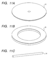
- phase plate 12 In order to realize a phase-contrast electron microscope, for example, there had heretofore been attempts to place a phase plate 12 using a thin film of low electric conductivity, which phase plate is substantially uniform in thickness and whose central portion is cut, on a back focal plane of an objective lens and give a phase shift to only a scattered wave caused by a specimen to thereby improve contrast as shown in Fig. 11(a).
- the phase plate having this construction has a drawback in that the thin film 12 is contaminated and charged up by the irradiation of an electron or electron beam to thereby produce an uncontrollable phase shift.
- phase plate Another drawback of the phase plate is that the scattered wave passes through the thin film 12 so that a variation in the thickness of the thin film 12 and the like occurs and the electron beam is placed under the influence of noise irrelevant to scattering caused by the specimen. Therefore, the present phase plate has not yet been put to practical use.
- phase plate has been also proposed wherein magnetic flux is enclosed within a ring 13 of a magnetic material for rotating the magnetic flux at its inside so as to prevent it from leaking to the outside, whereby phase contrast is applied to an electron transmitted through the inside and outside of the ring 13 by a vector potential using an AB-effect (see Japanese Patent Application Laid-Open No. 60-7048).
- This type of phase plate is different from the phase plate of the type using the aforementioned thin film and is excellent in that since the electron does not pass through the ring 13, the phase plate is not placed under the influence of those other than a phase shift.
- the present phase plate has not yet been put to practical use partly because it is difficult to adjust the amount of magnetic flux to be enclosed within the ring 13 to the magnitude or level necessary for the phase shift to be set to ⁇ /2, and partly because a method of manufacturing the phase plate is not yet established which is capable of reliably ensuring that the magnetic flux prevents from leaking to the outside of the ring 13. Also restrictions are imposed on the shape of the ring in principle due to the enclosure of the magnetic flux.
- An object of the present invention is to provide a phase plate capable of simultaneously solving the two problems referred to above and observing a phase object with contrast.
- Another object of the present invention is to provide a phase-contrast electron microscope having the phase plate referred to above.
- a further object of the present invention is to provide a phase-contrast electron microscope which makes an aberration correction possible by using the phase plate.
- the problem described in the paragraph (1) referred to above can be solved by utilizing the types such as the phase plates shown in Figs. 11(b) and 11(c) using the electrostatic potential or the vector potential rather than the type such as the thin-film type of Fig. 11(a), in which the electron or electron beam is transmitted through the phase plate over its entirety.
- the type using the electrostatic potential is adopted.
- the problem of the paragraph (2) that it is difficult to externally control the conventional type using the electrostatic potential can be solved by constructing such a structure that the electrostatic potential of the phase plate can be easily controlled using the micromachining technology.
- a device or phase plate, in analogy with the quarter wavelength phase plate of light, for changing the phase of an electron beam is needed to realize a phase-contrast electron microscope.
- the present invention proposes a phase plate having a structure capable of externally controlling an electrostatic potential in a vacuum in the vicinity of a focused electron beam corresponding to a direct wave formed on the optical axis of a back focal plane of an objective lens and also proposes a phase-contrast electron microscope using the phase plate.
- Fig. 1(a) shows the external appearance of a ring-shaped phase plate according to one embodiment of the present invention.
- the phase plate according to the present embodiment comprises a ring portion which serves as a phase plate and a support portion for mounting the phase plate that projects from the ring portion.
- the phase plate 100 according to the present embodiment is substantially shaped in the form of a layered structure composed of layers 1 through 5 as is the case in which a sectional structure thereof is shown in Fig. 1(b), a more specific structure thereof is illustrated in Fig. 2 and one example of a method of manufacturing the phase plate is shown in Fig. 6.
- the layers 1 through 5 respectively correspond to a conductor layer 1, an insulator layer 202, a conductor layer 303 and an insulator layer 402 as seen in Fig. 1(b).
- the outermost layers 1 and 5 provided on both sides are formed as conductor layers over their entirety.
- Two layers 2 and 4 provided inside the outermost layers 1 and 5 are constructed such that only outer peripheral portions 201 and 401 of ring portions are formed as conductor layers and other portions 202 and 402 are formed as insulator layers.
- a central layer 3 is constructed such that outer peripheral portions 301 are formed as conductor layers and the innermost peripheral portion 303 is formed as a conductor layer. Regions 302 provided between the outer peripheral portions 301 and the innermost peripheral portion 303 are defined as insulator layers.
- An inner surface of the conductor layer 303 of the central layer 3 serves as an electrode 8 to be described later and can be electrically connected to the outside through the support portion of the ring.
- the conductor layer 303 is formed as the innermost peripheral portion, it is exposed at the inner surface of the ring portion so as to function as the electrode 8.
- the electrode 8 is supplied with a predetermined potential for controlling an electrostatic potential produced inside the ring to a predetermined value.
- the present phase plate has a structure wherein as seen in the end on the left side of Fig. 1(a), a lead portion 101 of the electrode 8 is surrounded by conductor layers 103 with an insulating layer 102 interposed therebetween and as seen in the central portion of Fig. 1(a), only the electrode 8 is exposed to the inner surface of the ring.
- the phase plate 100 having such a structure By placing the phase plate 100 having such a structure on the optical axis of the back focal plane of the objective lens, grounding the conductor layers 103 surrounding the electrode 8 and controlling the potential at the electrode 8 to a required potential through the lead portion 101 of the support portion (a mechanism for electrically connecting the conductor layers 103 and the lead portion 101 of the electrode 8 to the outside so as to provide ground and a required potential is omitted from the drawing), the electron beam no longer charges up the insulator by directly contacting the insulator and hence a problem on the charge of the insulator can be resolved.
- the supply of the necessary potential to the lead portion 101 of the electrode permits the control of the electrostatic potential produced inside the ring to the predetermined value.
- the electron beam transmitted through the outside of the ring can substantially completely eliminate the influence of the electrostatic potential by the electrode 8 exposed to the inner surface of the ring.
- the electron beam transmitted inside the ring will cause a phase shift relative to the electron beam transmitted through the outside, which is proportional to a quantity obtained by integrating the electrostatic potential produced by the electrode 8 along the orbit of electrons.
- ⁇ ( ⁇ ) ( ⁇ e / ⁇ E ) ⁇ V ( ⁇ , z ) dz
- ⁇ radius extending from optical axis
- z coordinates on optical axis
- ⁇ ( ⁇ ) phase shift of electron at incident position ⁇
- e unit charge of electron
- ⁇ de Broglie wavelength of electron
- V( ⁇ ,z) axial-symmetrical electrostatic potential
- E energy of incident electron beam.
- the integration of the electrostatic potential is taken along the orbit of each electron.
- the electron beam to be used runs at extremely high speed and the electrostatic potential at the phase plate is low, then the electron beam may be regarded to enter substantially in parallel to the optical axis. For example, when an electron accelerated to several hundreds of kV or so is used and the potential at the electrode 8 is considered to be several volts V or so, this approximation is sufficiently established.
- the result of integration given by the above equation can take a constant value without depending on the incident position ⁇ of the electron where the electrostatic potential produced by the electrode 8 supplied with the potential is locally enclosed inside the ring by surrounding the periphery of the symmetry axis with the electrode 8 of the same potential and interposing the electrode 8 between other two electrodes 1 and 5 from both surfaces of the electrode 8.
- a quantity obtained by integrating a three-dimensional electrostatic potential in the direction of incidence of the electrons becomes a finite value and the resultant quantity complies with the two-dimensional Laplace's equation.
- a constant value is allowed inside the ring of the phase plate 100.
- the electron beam which passes through the inside of the ring of the phase plate 100, undergoes a predetermined phase shift relatively regardless of its incident position as compared with the electron beam that passes through the outside thereof.
- the potential to be applied to the electrode can be estimated quantitatively as follows.
- the integral term given in the above equation (1) can be estimated by the product of the potential supplied to the electrode and the thickness of the electrode.
- the potential at the electrode 8 may be set to 1V to bring the value of the above equation (1) to ⁇ /2 if inversely operated.
- the thickness of the electrostatic potential is kept constant without depending on the position of incidence of each electron as if a thin film of uniform thickness exist inside the ring.
- the direct wave can pass through the vacuum, a conventional problem does not arise that charging occurs due to contamination.
- the present embodiment takes note of the fact that the electron beam that passes through the inside of the ring, can provide the predetermined phase shift relatively regardless of its incident position as compared with the electron beam transmitted through the outside by surrounding the periphery of the optical axis for each electron with the ring-shaped electrode supplied with a uniform potential extremely low as compared with the accelerating voltage of each incident electron and interposing the electrode between the two other grounded ring-shaped electrodes so that the electrostatic potential produced by the electrode is localized inside the ring.
- This note will be of extreme importance to the phase-contrast electron microscope.
- the structure symmetrical as seen in the upward and downward directions is adopted wherein the central electrode is formed as the center and the openings of the conductor layers, which are defined inside the ring, are set equal in diameter to each other.
- the setting of the diameters of the ring-internally defined openings of the conductor layers 1 and 5 to the diameters smaller than that of the electrode 8 can prevent irradiation of insulator layers 7 exposed to the top and bottom of the electrode 8 with the electron beam and is also useful for preventing needless charging of the insulator layers 7 (corresponding to the portions designated at numerals 202 and 402 in Fig. 2) exposed to the ring inner surface.
- d f ⁇ /r
- the phase plate Since the phase plate is inserted into the position of the focal length of the objective lens and it is difficult to continuously vary it, the phase plate is set so as to be inserted into positions (e.g., positions of 10mm and 100mm) of focal lengths of several typical objective lenses, the focal lengths of the objective lenses are changed according to the size of a specimen to be observed and a phase plate corresponding to the changed focal length is used. It is thus possible to observe specimens different in size. At this time, it is necessary to vary an image-forming lens below the corresponding objective lens in interlock with it.
- the ratio between the direct wave and the scattered wave can be varied by changing the inside diameter of the ring. Namely, the more the inside diameter of the ring is decreased, the more the direct wave transmittable through the phase plate is reduced.
- each specimen can be observed under the change of the ratio between the direct wave and the scattered wave according to the intensity of scattering of the specimen by making switching between four or so many types of phase plates different in ring inside diameter, which are suitably spaced away from each other and arranged in series or on the perimeter of a predetermined diameter, by a movement or transfer mechanism.
- the contrast of an image at the time of the observation of the specimen can be improved by optimizing the ratio between the direct wave and the scattered wave.
- Fig. 3 shows the external appearance of a thin-wire shaped phase plate corresponding to one of other embodiments.
- the phase plate according to the present embodiment comprises a central portion from which a conductor 11 serving as the phase plate is exposed, and support portions for covering the conductor 11 with insulator layers 10 and provided with conductor layers 9 on their peripheries. Each support portion is used to mount the phase plate thereon and also serves as a lead portion extending to the exposed conductor 11 of the phase plate in tandem with this.
- the phase plate according to the present embodiment resembles the phase plate (see Fig. 11(c)) using the electrostatic potential, which has been introduced in the previously-cited paper, at first glance, the present phase plate is essentially different from the phase plate in that the electrostatic potential can be externally controlled.
- the phase plate according to the embodiment shown in Fig. 3 is different from that according to the embodiment shown in Fig. 1 and the potential exerts an influence on both the direct wave and the scattered wave.
- a predetermined phase shift can be approximately provided by controlling the potential at the conductor 11 and adjusting the electrostatic potential created by the conductor 11. Described more specifically, an electron microscope needs to take into consideration even a spherical aberration of an objective lens and a phase shift produced due to a focus displacement (called "defocus displacement or quantity”), thus resulting in the addition of these and the phase shift due to the aforementioned phase plate together. Even in that case, however, the electron microscope can be set to the optimum conditions by using a suitable defocus quantity according to a spherical aberration coefficient of the objective lens. Namely, the phase contrast can be uniformly raised in a wide spatial frequency range.
- the light and the electron beam serve as waves and can be described by two quantities of the amplitude and the phase. They will be described by reference to vector diagrams. Namely, the amplitude of the wave is represented as the length of a vector and the phase thereof is represented as an angle relative to a reference line of the vector.
- Fig. 4(a) shows a wave 15 (vector MA) incident to a specimen having absorption and a wave 16 (vector MD) transmitted through the specimen.
- the transmitted wave 16 changes in phase (angle) and amplitude (length) as compared with the incident wave 15.
- the transmitted wave 16 can be observed as an intensity difference with respect to the incident wave 15.
- This vector MD' shows a wave 18 scattered by the specimen.
- phase plate according to the present invention with respect to the electron beam also serves so as to vary the phase of the incident wave by ⁇ /2 in a manner precisely identical to the above and allow the scattered wave based on the specimen to pass therethrough as it is.
- a phase-contrast electron microscope is constructed by placing the phase plate on the back focal plane (position of objective diaphragm) of the objective lens of the conventional electron microscope or in the close vicinity of the back focal plane thereof, whereby the phase object such as a biological specimen can be observed with high contrast.
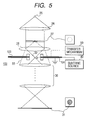
- Fig. 5 shows a basic configuration of an optical system of the present embodiment.
- the present microscope is basically similar in configuration to the normal electron microscope which comprises an electron source 25, a condenser lens 26, a specimen 27, an objective lens 28, an enlargement lens system 30, and an observing plane 31 of each of an image-sensing device and a display unit, for projecting or reflecting a fluorescent screen or an image on the fluorescent screen.
- a phase plate 100 is placed substantially in the optical axis in the vicinity of a back focal plane of the objective lens 28. Further, a conductor provided outside the phase plate 100 is grounded and a lead 101 extending to a central electrode 8 is supplied with a predetermined potential from an electric source 40.
- the phase plate 100 is formed as a structure wherein the phase plate 100 can be easily inserted into and withdrawn from the path of each electron by a vacuum transfer mechanism 50.
- the present microscope can be used as the normal electron microscope.
- the present microscope can be used as the phase-contrast electron microscope as shown in the drawing.
- phase-contrast electron microscope The operation of the phase-contrast electron microscope will next be described.
- An electron beam emitted from the electron source 25 enters the specimen 27 through the condenser lens 26.
- the electron beam 32 having the same amplitude and phase as those of the incident wave passes through the objective lens 28.
- the electron beam passes through the inside of the phase plate 100 at the back focal plane of the objective lens 28 so that the phase thereof is varied by ⁇ /2 + n ⁇ (n is determined according to the potential of the central electrode and the thickness thereof but adjusted so as to reach an integer).
- n is determined according to the potential of the central electrode and the thickness thereof but adjusted so as to reach an integer.
- Increasing n here is equivalent to an increase in the potential supplied to the central electrode of the phase plate.
- n is not necessarily limited to 0.
- an electron beam 33 subjected to scattering by the specimen (phase object) 27 and different in phase from the incident electron beam passes through the objective lens 28, followed by being transmitted through the outside of the phase plate 100 at the back focal plane of the objective lens 28.
- an image on the back focal plane of the objective lens 28 located in the phase plate 100 is focused on the observing plane 31 by the enlargement lens system 30 to obtain a diffraction image.
- the position of the phase plate 100 is automatically or manually adjusted so that the electron beam 32 having the same phase as that of the incident electron beam is transmitted through the inside of the phase plate 100.
- the two electron beams 32 and 33 form an enlarged image of the specimen 27 on the observing plane 31 through the enlargement lens system 30.
- the resultant image can be observed on the observing plane 31 as an image having an intensity difference, i.e., an image having large contrast.
- the resultant image can be observed as one having sufficient contrast if the contrast of the specimen itself is seen or taken in the form of a phase signal even if it little exists.
- Fig. 6 is a cross-sectional view of the phase plate taken along line B - B of Fig. 1 as seen in the direction indicated by arrows.
- Fig. 6(A) shows a state in which after anisotropic etching resistant films 61 and 63 have been evaporated onto both surfaces of a silicon substrate 62, a conductive film 64, an insulative film 65 and a conductive film 66 are successively layered on the upper surface of the anisotropic etching resistant film 63, and the insulative film 65 and the conductive film 66 are subjected to patterning.
- the conductive film 64, the insulative film 65 and the conductive film 66 have thicknesses of 250nm, 100nm and 250nm respectively.
- the anisotropic etching resistant films 61 and 63 are provided for the sake of forming a window and protecting a structure formed on the surface of the silicon substrate 62 from an etchant when anisotropic etching is effected on the silicon substrate 62 from the reverse side thereof.
- a silicon oxide film (SiO) or a silicon nitride film (SiN) or the like can be used for the anisotropic etching resistant films .
- the silicon oxide film (SiO) or the silicon nitride film (SiN) or the like can be used as the insulative film 65.
- any types may be used if suitable for purposes of insulation.
- the conductive films 64 and 66 gold, platinum, tungsten, aluminum, titanium or titanium nitride or the like can be used. However, any types may be used if suitable for purposes of conductors.
- Fig. 6(B) illustrates a state in which an anisotropic etching window 67 is patterned to the anisotropic etching resistant film 61 provided on the back of the silicon substrate 62 by a dry etching method using reactive gas with fluorine as the base.
- Fig. 6(C) shows a state in which an insulative film 68 of 100nm is deposited on the periphery of the upper conductive film 66 and is thereafter subjected to lithography by the dry etching method to thereby cover the conductive film 66 with the insulative film 68.
- Fig. 6(D) depicts a state in which a conductive film 69 of 250nm is further deposited on the periphery of the insulative film 68 of the conductive film 66 whose periphery has been surrounded by the insulative film 68, and is thereafter subjected to lithography by the dry etching method to thereby cover the insutlative film 68 with the conductive film 69, after which the ring central portion shown in Fig. 1 is defined by lithography.
- Fig. 6(E) shows a state in which anisotropic etching of silicon is carried out from the reverse side in a state in which the front surface has been protected, to thereby open or define a window of the silicon and thereafter the anisotropic etching resistant film 63 is removed by the dry etching method using the reactive gas with the fluorine as the base.
- phase plate shown in Fig. 1 is formed in this way, the formation of the phase plate is not limited to this method. It is needless to say that an arbitrary manufacturing method may be used for its formation.
- the conductive film 66 shown in Fig. 6(D) corresponds to the conductor layer 303 shown in Fig. 2
- the insulative film 68 corresponds to each of the insulator layers 202, 302 and 402
- the conductive film 69 corresponds to each of the conductor layers 1, 201, 301, 401 and 5.
- An electron microscope has a problem that although it has high resolution, the aberration of the electron lens, particularly, the spherical aberration of the objective lens cannot be corrected.
- the electron lens serves as a convex lens alone in principle unlike an optical lens capable of correcting aberration in accordance with a combination of a convex lens and a concave lens.
- Gabor's holography is most famous. Electron holography, which was hard to be realized due to the insufficiency of interference of an electron beam in those days of the invention by Gabor, has been put into practice with the advent of coherent electron source such as a field emission type electron gun in recent years.
- an aberration function of an objective lens is represented by two parameters of a spherical aberration coefficient of the objective lens and a defocus quantity under the following equation given using a wavelength ⁇ of an electron beam, the spherical aberration coefficient C s , the defocus quantity ⁇ and a scattering angle ⁇ .
- ⁇ ( ⁇ ) 2 ⁇ ⁇ - 1 4 ⁇ C s ⁇ 4 + 1 2 ⁇ 2
- the electron holography cannot reply to a question as to whether the estimated values of these two parameters are truly proper.
- a series of images is recorded by changing the defocus quantity and their spherical aberration is corrected by image processing of these images.
- the present method cannot similarly reply to a question as to whether the defocus quantity used for the photography is proper.
- the aberration is light-optically corrected after recording a hologram with the electron beam. Since both the amplitude and phase of an electron wave at an image plane are recorded, the aberration can be corrected anyway. In this case, however, this is performed on the major premise that the aberration function is already known.
- the aberration given by the equation (4) means so-called coherent aberration established when the interference of the electron or electron beam is complete. In fact, so-called incoherent aberration such as chromatic aberration or the like derived from the incomplete interference of the electron beam must be also considered together.
- phase plate of the present invention According to the phase plate of the present invention, these problems can be simultaneously resolved. It is also possible to obtain an ultra-high resolution image whose aberration has been corrected. Namely, the ultra-high resolution image can be easily realized by placing the phase plate on the optical axis of the back focal plane of the objective lens, recording a series of images providing different relative phase differences between the direct wave and the scattered wave and directly evaluating the aberration function of the lens from them.
- phase measuring methods employed in an optical interferometry such as a fringe-scanning method, a heterodyne method, a phase-lock method, etc. can be applied to the observation of the ultra-high resolution image of the weak phase object using the aforementioned phase plate.
- These methods have been described in the Applied Optics vol.13 (1974), p.2693, the Applied Optics vol.19 (1980), p.154, and the Optical Engineering vol.18 (1979), p.46. These will next be described. In the following description, a one-dimensional description will be used for simple illustration. Since a two-dimensional description causes only an increase in parameter, no generality is lost.
- a phase ⁇ (x) is precisely measured from the following interference-fringe intensity.
- I(x) a ( x )+ b ( x ) ⁇ sin( ⁇ ( x )+ ⁇ ( t ))
- ⁇ ( t ) sin ⁇ t
- I(x), a(x) and b(x) in the above equation (5) are represented as real variable functions.
- the respective methods can separate a(x) and b(x) from the measured interference-fringe intensity so as to precisely measure the phase ⁇ (x).
- the heterodyne method and the phase-lock method can effect specific modulation on the interference fringe in the same manner as the fringe-scanning method so as to precisely measure the phase.
- ⁇ indicates a coordinate in a Fourier space
- the use of the phase plate can permit the addition of the terms expressed in the equations (6), (7) and (8) to ⁇ ( ⁇ ) in the equation (14).
- Fig. 7 shows the structure of an embodiment of an electron microscope added with the aberration correction on the basis of the embodiment shown in Fig. 5.
- elements of structure identical or equivalent to those shown in Fig. 5 are identified by like reference numerals.
- an electron biprism 70 is added to a passage or path of an electron or electron beam.
- an image detector 72 is placed as an alternative to the observing plane 31.
- the biprism 70 is controlled by an electron biprism controller 71 capable of controlling the position of the biprism 70 and the voltage to be applied thereto.
- An output produced from the image detector 72 is processed by an image processor 74 and thereafter an image display device 73 displays an image picture of a specimen based on the output in a manner similar to the normal electron microscope.
- the electron biprism controller 71 and the image processor 74 are consistently controlled by a total controller 75 together with a transfer mechanism 50 for controlling the shift or movement of a phase plate 100 and the potential at the electrode 8 of the phase plate 100. It is needless to say that each of the biprism controller 71, the image processor 74 and the total controller 75 may be either of one having a so-called microcomputer incorporated therein and one in which the function of one computer is presented in separate form.
- the electron biprism 70 has a structure in which it can be easily withdrawn from or introduced into an electron path by the transfer mechanism in a manner similar to the phase plate 100.
- the electron biprism 70 is composed of a wire 701 used as an electrode and ground electrodes 702 and 703. Further, the electron biprism 70 is placed abovbe an enlargement lens system 30 but is used by being shifted to the path of the electron beam only when it is necessary to calibrate a phase shift corresponding to an electric potential of a phase plate to be described below.
- FIG. 8 A procedure for obtaining an image whose aberration has been corrected, using the phase plate utilizing the electrostatic potential shown in Fig. 1 will now be described with reference to Figs. 8, 9 and 10.
- the overall flow of process steps is illustrated in Fig. 8 as a flowchart. The process steps are controlled by the total controller 75.
- a phase shift corresponding to an electric potential of the phase plate 100 is first calibrated in Steps 81 and 82.
- the relationship between the phase shift corresponding to the electric potential of the phase plate 100 and the potential supplied to the phase plate 100 is already known in advance in some way, an operator gives the setting of its contents to the total controller 75. Therefore, the answer in Step 81 is YES, so that the routine procedure does not pass through Step 82 and hence proceeds to the next Step 83.
- Step 82 for the calibration of the phase shift will be shown in Fig. 9 as a flowchart.
- the electron biprism 70 is set in an electron path (Step 91).
- a current of a lens 30 is adjusted and the focal point of the electron microscope is focused to the phase plate 100 without being focused to a specimen 27 (Step 92).
- the position of the electron biprism 70 is adjusted and an electric potential is applied to the electrode 701 of the biprism 70 (Step 93).
- Step 94 equally-spaced interference patterns between electrons 120 transmitted through the inside of a ring of the phase plate 100 and electrons 110 transmitted through the outside thereof are observed (Step 94).
- a phase shift corresponding to an electric potential of the phase plate 100 still remains nothing and hence the interference pattern are arranged in a straight line inside and outside the ring.
- a shadow designated at numeral 100 corresponds to a ring portion of the phase plate 100.
- the interference patterns are arranged again in a straight line inside and outside the ring as designated at numerals 140 in Fig. 10(c).
- the phase shift corresponding to the electric potential of the phase plate 100 corresponds to one wavelength at this time.
- An electric potential V 0 required to supply a phase shift corresponding to one wavelength of an electron can be precisely measured by further increasing the voltage and measuring several potentials at which the interference patterns are arranged in the straight line (Step 96).
- the electric potential may be either positive or negative.
- the direction of transfer of each interference pattern inside the ring is simply reversed between the positive and negative potentials.
- the absolute value V 0 of the potential required to provide the phase shift equivalent to one wavelength of the electron is made identical.
- the lens current is reset (Step 97).
- the unnecessary biprism is shifted to the outside from the electron path (Step 98).
- the calibration of the phase shift is terminated in this way.
- Step 83 It is next determined in Step 83 whether the electron beam, which has converged on the back focal plane of the objective lens 28, passes through just the center of the ring of the phase plate 100. If the electron beam is found not to pass through the center of the ring of the phase plate, it is then determined that it is necessary to perform the alignment of the phase plate 100. Thereafter, its alignment is executed in Step 84.
- a current of a image-formation or focusing lens 30 is adjusted to align the focal point of the electron microscope with the phase plate 100 inserted into the back focal plane of the objective lens. The position of the phase plate is shifted so that the electron beam focused onto the back focal plane of the objective lens 28 passes through just the center of the ring of the phase plate.
- the lens current is adjusted to align the focal point of the electron microscope with the specimen.
- Step 85 When the alignment of the phase plate is completed, one is selected from the methods used for the aforementioned aberration correction (Step 85). The following description will be made on the assumption that the fringe-scanning method has been selected.
- M (M ⁇ 2) images are required in total.
- the number of M can be selected by an observer but may range from normally about 10 to 100.
- Step 86 images Q (x, y; n) obtained when the potential V(n) given by the equation (22) or (24) is applied to the phase plate 100, are successively detected by the image detector and stored in the image processor 74.
- x and y indicate two-dimensional coordinates for respective pixels of each image.
- Step 87 it is determined in Step 87 whether the required number of images has been obtained.
- Step 88 two-dimensional Fourier transforms of a series of images are calculated to obtain a series of real parts r ( ⁇ , ⁇ ; n)and imaginary parts i ( ⁇ , ⁇ ; n). Thereafter, an aberation-corrected image is displayed.
- ⁇ and ⁇ are coordinates in a two-dimensional Fourier space.
- the unknown aberration function can be precisely determined.
- the aberration function is determined in this way, an image or hologram is photographed under conditions in which the aberration is already known, so that an image whose aberration has been corrected, can be calculated from it. Further, the approximation of the determined aberration function to the equation (4) also permits determination of a spherical aberration and a defocus quantity.
- the present embodiment has described the phase plate having the ring structure shown in Fig. 1 by using the fringe-scanning method as an example. It is however needless to say that the present processing can be executed even in the case of the phase plate using other method or the phase plate having the structure shown in Fig. 3.
- a phase plate capable of observing a specimen (phase object) low in amplitude contrast, such as a biological specimen as an image with high contrast without heavy-metal staining, and a phase-contrast electron microscope using the phase plate can be realized in a manner similar to an optical phase-contrast microscope owing to the mounting of the phase plate to the normal electron microscope as an additional means,
Landscapes
- Chemical & Material Sciences (AREA)
- Analytical Chemistry (AREA)
- Analysing Materials By The Use Of Radiation (AREA)
- Electron Sources, Ion Sources (AREA)
Applications Claiming Priority (2)
| Application Number | Priority Date | Filing Date | Title |
|---|---|---|---|
| JP34027095 | 1995-12-27 | ||
| JP340270/95 | 1995-12-27 |
Publications (2)
| Publication Number | Publication Date |
|---|---|
| EP0782170A2 true EP0782170A2 (fr) | 1997-07-02 |
| EP0782170A3 EP0782170A3 (fr) | 1998-04-08 |
Family
ID=18335340
Family Applications (1)
| Application Number | Title | Priority Date | Filing Date |
|---|---|---|---|
| EP96120384A Withdrawn EP0782170A3 (fr) | 1995-12-27 | 1996-12-18 | Microscope électronique à contraste de phase et plaque de phase pour un tel microscope |
Country Status (2)
| Country | Link |
|---|---|
| US (1) | US5814815A (fr) |
| EP (1) | EP0782170A3 (fr) |
Cited By (7)
| Publication number | Priority date | Publication date | Assignee | Title |
|---|---|---|---|---|
| DE10206703A1 (de) * | 2002-02-18 | 2003-08-28 | Max Planck Gesellschaft | Phasenplatte für die Elektronenmikroskopie und elektronenmikroskopische Bildgebung |
| WO2006017252A1 (fr) * | 2004-07-12 | 2006-02-16 | The Regents Of The University Of California | Amelioration de phase pour microscope electronique |
| DE102005040267A1 (de) * | 2005-08-24 | 2007-03-01 | Universität Karlsruhe | Verfahren zum Herstellen einer mehrschichtigen elektrostatischen Linsenanordnung |
| DE102006055510A1 (de) * | 2006-11-24 | 2008-05-29 | Ceos Corrected Electron Optical Systems Gmbh | Phasenplatte, Bilderzeugungsverfahren und Elektronenmikroskop |
| EP1959475A2 (fr) | 2007-02-14 | 2008-08-20 | Carl Zeiss NTS GmbH | Elément à décalage de phase et appareil de rayonnement à particules doté d'un élément de à décalage de phase |
| DE102008037698A1 (de) | 2008-08-14 | 2010-02-18 | Carl Zeiss Nts Gmbh | Elektronenmikroskop mit ringförmiger Beleuchtungsapertur |
| EP1950789A4 (fr) * | 2005-11-04 | 2011-05-11 | Nagayama Ip Holdings Llc | Plaque de phase pour microscope electronique et son procede de fabrication |
Families Citing this family (30)
| Publication number | Priority date | Publication date | Assignee | Title |
|---|---|---|---|---|
| US6819435B2 (en) * | 2000-04-12 | 2004-11-16 | Nano Or Technologies Inc. | Spatial and spectral wavefront analysis and measurement |
| JP3942363B2 (ja) * | 2001-02-09 | 2007-07-11 | 日本電子株式会社 | 透過電子顕微鏡の位相板用レンズシステム、および透過電子顕微鏡 |
| DE10200645A1 (de) | 2002-01-10 | 2003-07-24 | Leo Elektronenmikroskopie Gmbh | Elektronenmikroskop mit ringförmiger Beleuchtungsapertur |
| US7609388B2 (en) * | 2002-01-24 | 2009-10-27 | Icos Vision Systems Nv | Spatial wavefront analysis and 3D measurement |
| US7365909B2 (en) * | 2002-10-17 | 2008-04-29 | Xradia, Inc. | Fabrication methods for micro compounds optics |
| US7119953B2 (en) * | 2002-12-27 | 2006-10-10 | Xradia, Inc. | Phase contrast microscope for short wavelength radiation and imaging method |
| JP4625317B2 (ja) * | 2004-12-03 | 2011-02-02 | ナガヤマ アイピー ホールディングス リミテッド ライアビリティ カンパニー | 位相差電子顕微鏡用位相板及びその製造方法並びに位相差電子顕微鏡 |
| JP4600239B2 (ja) * | 2005-10-07 | 2010-12-15 | 株式会社日立製作所 | 磁性電子顕微鏡 |
| DE102006011615A1 (de) | 2006-03-14 | 2007-09-20 | Carl Zeiss Nts Gmbh | Phasenkontrast-Elektronenmikroskop |
| EP2091062A1 (fr) | 2008-02-13 | 2009-08-19 | FEI Company | TEM avec correcteur d'aberrations et lame de phase |
| EP2131385A1 (fr) | 2008-06-05 | 2009-12-09 | FEI Company | Plaque de phase hybride |
| US7977633B2 (en) * | 2008-08-27 | 2011-07-12 | Max-Planck-Gesellschaft Zur Foerderung Der Wissenschaften E. V. | Phase plate, in particular for an electron microscope |
| JP4896106B2 (ja) * | 2008-09-30 | 2012-03-14 | 株式会社日立ハイテクノロジーズ | 電子顕微鏡 |
| NL2004888A (en) * | 2009-06-29 | 2010-12-30 | Asml Netherlands Bv | Deposition method and apparatus. |
| EP2299468A1 (fr) * | 2009-09-20 | 2011-03-23 | Universiteit Antwerpen | Procédés et systèmes pour utiliser des plaques de phase |
| US8785850B2 (en) * | 2010-01-19 | 2014-07-22 | National Research Counsel Of Canada | Charging of a hole-free thin film phase plate |
| JP5564292B2 (ja) * | 2010-03-05 | 2014-07-30 | 株式会社日立製作所 | 位相板およびこれを用いた位相差電子顕微鏡 |
| WO2011163397A1 (fr) * | 2010-06-22 | 2011-12-29 | The Regents Of The University Of California | Ouverture de foucault passe-haut micro-usinée pour microscopie électronique |
| EP2400522A1 (fr) | 2010-06-24 | 2011-12-28 | Fei Company | Élément de blocage pour une utilisation dans le plan de diffraction d'un TEM |
| EP2485239A1 (fr) | 2011-02-07 | 2012-08-08 | FEI Company | Procédé de centrage d'un élément optique dans un TEM comprenant un élément d'amélioration du contraste |
| JP5745957B2 (ja) * | 2011-07-01 | 2015-07-08 | 株式会社日立ハイテクノロジーズ | 位相板、および電子顕微鏡 |
| EP2624278B1 (fr) * | 2012-01-31 | 2014-07-30 | Hitachi High-Technologies Corporation | Plaque de phase |
| JP5836171B2 (ja) * | 2012-03-21 | 2015-12-24 | 日本電子株式会社 | 透過型電子顕微鏡の調整方法 |
| JP6286270B2 (ja) | 2013-04-25 | 2018-02-28 | エフ イー アイ カンパニFei Company | 透過型電子顕微鏡内で位相版を用いる方法 |
| DE102013019297A1 (de) | 2013-11-19 | 2015-05-21 | Fei Company | Phasenplatte für ein Transmissionselektronenmikroskop |
| EP2887381B1 (fr) | 2013-12-18 | 2016-09-21 | Fei Company | Procédé d'investigation du front d'onde d'un faisceau de particules chargées |
| JP6418706B2 (ja) * | 2014-07-30 | 2018-11-07 | フォルシュングスツェントルム・ユーリッヒ・ゲゼルシャフト・ミット・ベシュレンクテル・ハフツング | 荷電粒子画像化システム用の調整可能なアンペア位相板 |
| EP3474308A1 (fr) | 2017-10-17 | 2019-04-24 | Universiteit Antwerpen | Manipulation de phase spatiale d'un faisceau de particules chargées |
| JP6876654B2 (ja) * | 2018-07-03 | 2021-05-26 | 日本電子株式会社 | 電子顕微鏡 |
| JP7641528B2 (ja) * | 2021-05-21 | 2025-03-07 | パナソニックIpマネジメント株式会社 | 位相差顕微鏡 |
Citations (1)
| Publication number | Priority date | Publication date | Assignee | Title |
|---|---|---|---|---|
| US4935625A (en) * | 1987-09-04 | 1990-06-19 | Hitachi, Ltd. | Electron holography apparatus |
Family Cites Families (4)
| Publication number | Priority date | Publication date | Assignee | Title |
|---|---|---|---|---|
| DE1564075B1 (de) * | 1966-05-13 | 1970-04-30 | Karl-Josef Dr Rer Nat Hanssen | Verfahren zur kontrastreichen Abbildung von Phasen- oder Amplitudenobjekten in einem Korpuskularstrahlgeraet,insbesondere einem Elektronenmikroskop |
| DE1810818A1 (de) * | 1968-04-16 | 1969-10-23 | Prof Dr Walter Hoppe | Korpuskularstrahlgeraet mit einer Abbildungslinse und einer dieser zugeordneten phasenschiebenden Folie |
| JPS607048A (ja) * | 1983-06-24 | 1985-01-14 | Hitachi Ltd | 位相差電子顕微鏡 |
| JP2966474B2 (ja) * | 1990-05-09 | 1999-10-25 | 株式会社日立製作所 | 電子線ホログラフィ装置 |
-
1996
- 1996-12-17 US US08/768,355 patent/US5814815A/en not_active Expired - Fee Related
- 1996-12-18 EP EP96120384A patent/EP0782170A3/fr not_active Withdrawn
Patent Citations (1)
| Publication number | Priority date | Publication date | Assignee | Title |
|---|---|---|---|---|
| US4935625A (en) * | 1987-09-04 | 1990-06-19 | Hitachi, Ltd. | Electron holography apparatus |
Non-Patent Citations (3)
| Title |
|---|
| "A New Electron Microscope Imaging Method for Enhancing Detail in Thin Biological Specimens.", Z. NATURFORSCH., vol. 29A, 1974, pages 158 - 163 |
| BOERSCH H: "Über die Kontraste von Atomen im Elektronenmikroskop", ZEITSCHRIFT FÜR NATURFORSCHUNG, vol. 2A, 18 June 1947 (1947-06-18), pages 615 - 633, XP009150730 * |
| PHYS. REV. LETT., vol. 74, 1995, pages 399 |
Cited By (17)
| Publication number | Priority date | Publication date | Assignee | Title |
|---|---|---|---|---|
| DE10206703A1 (de) * | 2002-02-18 | 2003-08-28 | Max Planck Gesellschaft | Phasenplatte für die Elektronenmikroskopie und elektronenmikroskopische Bildgebung |
| WO2003068399A3 (fr) * | 2002-02-18 | 2004-02-05 | Max Planck Gesellschaft | Lame de phase pour la microscopie electronique et imagerie par microscopie electronique |
| WO2006017252A1 (fr) * | 2004-07-12 | 2006-02-16 | The Regents Of The University Of California | Amelioration de phase pour microscope electronique |
| US7737412B2 (en) | 2004-07-12 | 2010-06-15 | The Regents Of The University Of California | Electron microscope phase enhancement |
| WO2007022862A3 (fr) * | 2005-08-24 | 2007-05-03 | Univ Karlsruhe | Procede de fabrication d'un ensemble lentilles electrostatique a plusieurs couches |
| DE102005040267B4 (de) * | 2005-08-24 | 2007-12-27 | Universität Karlsruhe | Verfahren zum Herstellen einer mehrschichtigen elektrostatischen Linsenanordnung, insbesondere einer Phasenplatte und derartige Phasenplatte |
| DE102005040267A1 (de) * | 2005-08-24 | 2007-03-01 | Universität Karlsruhe | Verfahren zum Herstellen einer mehrschichtigen elektrostatischen Linsenanordnung |
| US8487268B2 (en) | 2005-08-24 | 2013-07-16 | Dagmar Gerthsen | Method for the production of multiplayer electrostatic lens array |
| EP1950789A4 (fr) * | 2005-11-04 | 2011-05-11 | Nagayama Ip Holdings Llc | Plaque de phase pour microscope electronique et son procede de fabrication |
| DE102006055510A1 (de) * | 2006-11-24 | 2008-05-29 | Ceos Corrected Electron Optical Systems Gmbh | Phasenplatte, Bilderzeugungsverfahren und Elektronenmikroskop |
| WO2008061603A3 (fr) * | 2006-11-24 | 2008-07-10 | Ceos Gmbh | Lame de phase, procédé d'imagerie et microscope électronique |
| DE102006055510B4 (de) * | 2006-11-24 | 2009-05-07 | Ceos Corrected Electron Optical Systems Gmbh | Phasenplatte, Bilderzeugungsverfahren und Elektronenmikroskop |
| US7928379B2 (en) | 2006-11-24 | 2011-04-19 | Ceos Corrected Electron Optical Systems Gmbh | Phase plate, imaging method, and electron microscope |
| EP1959475A2 (fr) | 2007-02-14 | 2008-08-20 | Carl Zeiss NTS GmbH | Elément à décalage de phase et appareil de rayonnement à particules doté d'un élément de à décalage de phase |
| DE102007007923A1 (de) | 2007-02-14 | 2008-08-21 | Carl Zeiss Nts Gmbh | Phasenschiebendes Element und Teilchenstrahlgerät mit phasenschiebenden Element |
| US7902506B2 (en) | 2007-02-14 | 2011-03-08 | Carl Zeiss Nts Gmbh | Phase-shifting element and particle beam device having a phase-shifting element |
| DE102008037698A1 (de) | 2008-08-14 | 2010-02-18 | Carl Zeiss Nts Gmbh | Elektronenmikroskop mit ringförmiger Beleuchtungsapertur |
Also Published As
| Publication number | Publication date |
|---|---|
| EP0782170A3 (fr) | 1998-04-08 |
| US5814815A (en) | 1998-09-29 |
Similar Documents
| Publication | Publication Date | Title |
|---|---|---|
| US5814815A (en) | Phase-contrast electron microscope and phase plate therefor | |
| Majorovits et al. | Optimizing phase contrast in transmission electron microscopy with an electrostatic (Boersch) phase plate | |
| JP5560242B2 (ja) | 荷電粒子のビームにより表面を調査又は改変する装置及び方法 | |
| US6674078B2 (en) | Differential contrast transmission electron microscope and method of processing data about electron microscope images | |
| EP2333809B1 (fr) | Microscope électronique | |
| US20020011566A1 (en) | Thin-film phase plate, phase-contrast electron microscope using same, and method of preventing charging of phase plate | |
| US9202670B2 (en) | Method of investigating the wavefront of a charged-particle beam | |
| US8772715B2 (en) | Electron beam device including a first electron biprism to split an electron beam into two beams and a second electron biprism in the image forming lens system to superpose the two beams | |
| McCartney et al. | Quantitative measurement of nanoscale electrostatic potentials and charges using off-axis electron holography: Developments and opportunities | |
| JPH09237603A (ja) | 位相差電子顕微鏡およびその位相板 | |
| JP3039563B2 (ja) | 走査電子顕微鏡及び走査電子顕微方法 | |
| US7750298B2 (en) | Interferometer having three electron biprisms | |
| Dunin-Borkowski et al. | Conventional and back-side focused ion beam milling for off-axis electron holography of electrostatic potentials in transistors | |
| US7816648B2 (en) | Electron interferometer or electron microscope | |
| EP3067912A1 (fr) | Plaque de phase, son procédé de fabrication et microscope électronique | |
| Jorden et al. | Nonuniformity of CCDs and the effects of spatial undersampling | |
| US7015469B2 (en) | Electron holography method | |
| Tamaki et al. | Near-field electron ptychography using full-field structured illumination | |
| Hirayama et al. | Interference of three electron waves by two biprisms and its application to direct visualization of electromagnetic fields in small regions | |
| US10948426B2 (en) | Particle beam device, observation method, and diffraction grating | |
| Weiss et al. | A study of small electron probe formation in a field emission gun TEM/STEM | |
| JP2022071166A (ja) | 透過電子顕微鏡 | |
| EP4411783A1 (fr) | Holographie basée sur microscopie électronique à basse énergie | |
| Kimoto et al. | Practical procedure for coma-free alignment using caustic figure | |
| JPH0381939A (ja) | 走査干渉電子顕微鏡 |
Legal Events
| Date | Code | Title | Description |
|---|---|---|---|
| PUAI | Public reference made under article 153(3) epc to a published international application that has entered the european phase |
Free format text: ORIGINAL CODE: 0009012 |
|
| AK | Designated contracting states |
Kind code of ref document: A2 Designated state(s): DE NL |
|
| PUAL | Search report despatched |
Free format text: ORIGINAL CODE: 0009013 |
|
| AK | Designated contracting states |
Kind code of ref document: A3 Designated state(s): DE NL |
|
| 17P | Request for examination filed |
Effective date: 19981001 |
|
| 17Q | First examination report despatched |
Effective date: 19990617 |
|
| STAA | Information on the status of an ep patent application or granted ep patent |
Free format text: STATUS: THE APPLICATION IS DEEMED TO BE WITHDRAWN |
|
| 18D | Application deemed to be withdrawn |
Effective date: 20020104 |