EP2400522A1 - Élément de blocage pour une utilisation dans le plan de diffraction d'un TEM - Google Patents
Élément de blocage pour une utilisation dans le plan de diffraction d'un TEM Download PDFInfo
- Publication number
- EP2400522A1 EP2400522A1 EP10167258A EP10167258A EP2400522A1 EP 2400522 A1 EP2400522 A1 EP 2400522A1 EP 10167258 A EP10167258 A EP 10167258A EP 10167258 A EP10167258 A EP 10167258A EP 2400522 A1 EP2400522 A1 EP 2400522A1
- Authority
- EP
- European Patent Office
- Prior art keywords
- blocking member
- electron microscope
- transmission electron
- electrons
- plane
- Prior art date
- Legal status (The legal status is an assumption and is not a legal conclusion. Google has not performed a legal analysis and makes no representation as to the accuracy of the status listed.)
- Withdrawn
Links
Images

Classifications
-
- H—ELECTRICITY
- H01—ELECTRIC ELEMENTS
- H01J—ELECTRIC DISCHARGE TUBES OR DISCHARGE LAMPS
- H01J37/00—Discharge tubes with provision for introducing objects or material to be exposed to the discharge, e.g. for the purpose of examination or processing thereof
- H01J37/26—Electron or ion microscopes; Electron or ion diffraction tubes
- H01J37/261—Details
- H01J37/263—Contrast, resolution or power of penetration
-
- H—ELECTRICITY
- H01—ELECTRIC ELEMENTS
- H01J—ELECTRIC DISCHARGE TUBES OR DISCHARGE LAMPS
- H01J37/00—Discharge tubes with provision for introducing objects or material to be exposed to the discharge, e.g. for the purpose of examination or processing thereof
- H01J37/02—Details
- H01J37/04—Arrangements of electrodes and associated parts for generating or controlling the discharge, e.g. electron-optical arrangement or ion-optical arrangement
- H01J37/09—Diaphragms; Shields associated with electron or ion-optical arrangements; Compensation of disturbing fields
-
- H—ELECTRICITY
- H01—ELECTRIC ELEMENTS
- H01J—ELECTRIC DISCHARGE TUBES OR DISCHARGE LAMPS
- H01J2237/00—Discharge tubes exposing object to beam, e.g. for analysis treatment, etching, imaging
- H01J2237/04—Means for controlling the discharge
- H01J2237/043—Beam blanking
-
- H—ELECTRICITY
- H01—ELECTRIC ELEMENTS
- H01J—ELECTRIC DISCHARGE TUBES OR DISCHARGE LAMPS
- H01J2237/00—Discharge tubes exposing object to beam, e.g. for analysis treatment, etching, imaging
- H01J2237/22—Treatment of data
- H01J2237/221—Image processing
- H01J2237/223—Fourier techniques
-
- H—ELECTRICITY
- H01—ELECTRIC ELEMENTS
- H01J—ELECTRIC DISCHARGE TUBES OR DISCHARGE LAMPS
- H01J2237/00—Discharge tubes exposing object to beam, e.g. for analysis treatment, etching, imaging
- H01J2237/26—Electron or ion microscopes
- H01J2237/2614—Holography or phase contrast, phase related imaging in general, e.g. phase plates
-
- H—ELECTRICITY
- H01—ELECTRIC ELEMENTS
- H01J—ELECTRIC DISCHARGE TUBES OR DISCHARGE LAMPS
- H01J2237/00—Discharge tubes exposing object to beam, e.g. for analysis treatment, etching, imaging
- H01J2237/26—Electron or ion microscopes
- H01J2237/28—Scanning microscopes
- H01J2237/2802—Transmission microscopes
Definitions
- the invention relates to a transmission electron microscope for imaging a sample, the transmission electron microscope showing a diffraction plane in which a diffraction pattern of the sample is formed, the diffraction pattern representing an image of the sample in the Fourier domain, the transmission electron microscope comprising a blocking member positioned in the diffraction plane or an image thereof, the blocking member blocking a part of the Fourier domain, the blocked part of the Fourier domain in at least one direction extending from a low spatial frequency to a high spatial frequency.
- TEM Transmission Electron Microscope
- TEM Transmission Electron Microscope
- phase contrast occurs as a result of the interference of electrons that pass through the sample unhindered with elastically scattered electrons.
- Phase contrast typically occurs when the sample comprises little heavy atoms and many light atoms, such as carbon, hydrogen, etc., It is noted that in phase contrast the energy of the electrons is hardly changed and it is therefore also referred to as elastic deflection.
- the phase contrast of a TEM is often expressed by the Contrast Transfer Function (CTF), which expresses the contrast as a function of the spatial frequency.
- CTF Contrast Transfer Function
- the CTF in turn can be described as the product of two sub-functions: the envelope function and the Phase Contrast Transfer Function, with both these functions also a function of the spatial frequency.
- a detailed description of these functions, and their interdependency, is found in " Electron Crystallography of Biological Macromolecules", R.M. Glaeser et al. (2007), Oxford University Press, ISBN 978-0-19-508871-7 , hereby incorporated by reference. More specifically in page 67-72, paragraphs 3.8 and 3.9:,
- the Phase Contrast Transfer Function is among others a function of the defocus of the lens imaging the sample, and thus of the distance from the sample to the focal plane of the lens.
- users of a TEM often operate at the so-called Scherzer defocus.
- Glaeser describes the well-known Scherzer defocus (see also fig.3 . 4 of said publication) and the resulting phase contrast transfer function (see e.g. fig. 3 . 5 of said publication).
- the phase contrast transfer function shows oscillations between +1 and -1, and therefore the CTF shows similar oscillations.
- the Scherzer defocus is often used as it shows a large frequency band where the CTF is continuously positive (above zero).
- the first zero crossing at Scherzer defocus is typically at a spatial frequency above 3 nm -1 , corresponding with a resolution in the image of 0.3 nm (3 ⁇ ngstrom). Such a resolution is typically considered sufficient for biological imaging.
- the CTF is low for low spatial frequencies. This implies that in images of a sample showing phase contrast large structures are hard to detect.
- a disadvantage of the single side band method is that the achieved contrast is at best 50% of the envelope.
- the present invention presents a method in which the CTF in a large frequency band equals 50% of the envelope function, and for a large frequency band substantially more than 50% of the envelope function.
- the TEM according to the invention is characterized in that the high spatial frequency blocked by the blocking member is lower than or equal to the lowest spatial frequency where an image of said diffraction plane imaged without the blocking member shows a Contrast Transfer Function of approximately 50%.
- the blocking member does not block electrons that are deflected/scattered over a larger angle (the electrons contributing to a high spatial frequency). This implies that for a spatial frequency above said high spatial frequency the CTF shows it normal behavior, at first rising to a value larger than 0.5 (thus showing more contrast than available in SSB imaging) and then starting its oscillations.
- the invention thus combines good contrast at low spatial frequencies with the higher contrast available for other spatial frequencies in e.g. the Scherzer defocus.
- phase plates as e.g. described in US patent No. US 5,814,815 to Hitachi and US patent No. 6,674,078 to JEOL .
- a phase plate is used to realize a phase shift between the undiffracted electrons with respect to the diffracted electrons, analogous to the working of a Zernike phase plate in light optics.
- the blocking member needs to stop (absorb) the electrons impinging thereon, or scatter the electrons under a large angle. Therefore the blocking member typically comprises a heavy metal for stopping/scattering/absorbing the electrons.
- the blocking member is connected to one or more support arms.
- the one or more support arm supports the blocking member and connect it to a more macroscopic structure, so that it can be positioned with, for example, a positioning system as used for apertures in a TEM .
- the one or more support arms should be rigid enough, but on the other hand it should intercept as little electrons as possible.
- the support used also intercepts electrons, thereby resulting in a lower contrast in that direction and frequency. Therefore the support arms should cover as little space in the diffraction plane as possible.
- the blocking member is supported by a thin film, said film transparent to the impinging electrons.
- Such supporting films such as carbon films, graphene films, or thin silicon film are known to the person skilled in the art.
- the film is preferable electrically conductive, as otherwise charging occurs.
- the blocking member resembles a rectangle.
- the blocking member By forming the blocking member in the form of a rectangle, a blocking member with a straight edge is formed. By positioning the beam of undiffracted (undeflected) electrons just beside the straight edge such that this beam does not impinge thereon, part of the Fourier space is blocked, resulting in the partial SSB imaging.
- the blocking structure is a rectangle, the blocked space is not in all directions identical. That is only the case in a structure where the outer diameter is formed at a constant distance from the undiffracted beam.
- the blocking member resembles a trapezoid with varying width, wherein the diffraction pattern shows a spot of undiffracted electrons, and the blocked spatial frequency interval is chosen by positioning the beam of undiffracted electrons near a part of the blocking member with an appropriate width.
- the size of the diffraction pattern depends on the energy of the electrons impinging on the sample: a higher energy results in a smaller size of the diffraction pattern.
- the defocus used influences the spatial frequency where the CTF reaches a value of 0.5. This implies that the size of the area of the diffraction plane to be blanked should preferably be tunable as well.
- the blocking member shows a beam with a discrete number of steps, each with a different width.
- the width appropriate for e.g. the electron energy used can be selected in discrete values.
- the blocking member resembles a half-circle.
- this embodiment has a high frequency that is equal in all directions.
- the half-circle shows a straight edge, and the support arm extends perpendicular or parallel to said straight edge.
- the blocking member is placed in a plane that is an image of the diffraction plane and where an anamorphotic image of the diffraction plane is formed.
- the plane where an anamorphotic image is formed results in a plane where the diffraction pattern is imaged as a number of stripes, instead of points. This results in lower peak current densities. This may be preferable when avoiding contamination, damage, or other current density related issues.
- the blocking member is placed in a plane that is an image of the diffraction plane and the imaging of the diffraction plane onto the said plane is at least in part realized by transfer optics that are part of corrector optics, the corrector optics for correcting the aberrations of the lens forming the diffraction pattern.
- correctors are typically equipped with transfer optics. By combining transfer optics that image the diffraction plane with the transfer optics used for a corrector, a compact design is realized.
- At least part of the blocking member is electrically isolated from earth and electrically connected to a current measurement unit for measuring the current impinging on at least a part of the blocking member.
- the current measurement is used to position the beam of undiffracted electrons with respect to the blocking member.
- the transmission electron microscope further comprises means for heating the blocking member.
- Heating the blocking member is used to avoid contamination and/or clean the blocking member when contamination occurred. Hereby e.g. charging of the blocking member is kept to a minimum.
- the diffraction pattern shows a spot of undiffracted electrons and the blocking member shows an indent at the location where the beam of undiffracted electrons is closest to the blocking member, as a result of which contamination of the blocking member is reduced.
- a method of using of a blocking member in a transmission electron microscope comprising:
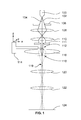
- Figure 1 schematically shows a TEM.
- the TEM comprises an electron source 100 producing a beam of electrons 102 round optical axis 104.
- the amount of electrons accepted from the source is governed by aperture 106.
- Condenser lenses 108 and 110 then form a parallel beam of electrons, from which aperture 111 I accepts a part. Herewith a parallel beam of electrons is formed.
- This beam irradiates the sample 112, that is positioned on positioning unit 114.
- the positioning unit enables the sample to be moved in the x,y, and z direction, as well as rotate round the x-axis.
- Objective lens 116 then forms an enlarged image of the object at first image plane 119, which enlarged image is further enlarged by lenses 120 and 122 and projected on sensor 124.
- Sensor 124 may be a camera, but also fluorescent screens are used.
- the objective lens also forms a diffraction pattern in the diffraction plane 118.
- this description shows the TEM operating in TEM mode, where a parallel beam illuminates the sample and the sample is imaged.
- a TEM is typically equipped to work in many other modes as well, including modes where the sample is illuminated with convergent of divergent beams, beams focused on and scanned over the sample, imaging of the diffraction plane on the sensor, etc.
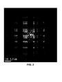
- Figure 2 shows a diffraction pattern
- the diffraction pattern shown here is of a crystalline material, as is evident of the spots shown. It shows a strong central spot, formed by the undiffracted electrons, surrounded by a large number of spots formed by diffracted electrons. Due to the crystalline nature of the sample used here, there is a strong preference for electrons to be scattered under specific directions. It is noted that an amorphous sample (as most biological samples are) would show a diffuse distribution of the electron surrounding the central peak.
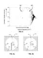
- Figure 3 schematically shows the Contrast Transfer Function of an objective lens.
- Figure 3 shows a graph of the CTF 301 in the so-named Scherzer focus. It shows that for low spatial frequencies of less than 1 nm -1 , the function is less 0.5, dropping to zero when going to a spatial frequency of zero. Therefore large structures, in this case larger than e.g. 1 nm, become less visible. For e.g. biologists this means that, although they can make images with high resolution, it is difficult to relate the high resolution observations with more macroscopic structures like organelles.
- the frequency where the function crosses the x-axis, and the amplitude of the envelope function as a function of frequency, are dependent on the quality of the lens.
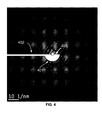
- Figure 4 schematically shows the diffraction pattern of figure 2 overlaid with the blocking member.
- Figure 4 shows the diffraction pattern shown in figure 2 , on which a blocking member 401 is projected.
- the blocking member is connected to a more macroscopic structure (and eventually the TEM) by support arm 402.
- the blocking member is here formed as a half-circle with a straight edge 403. In the centre of the circle an indent is formed where the undiffracted beam can pass, so that these electrons do not impinge on the blocking member. This indent ensures a low frequency behavior of the blocking member for a low frequency that is identical in all directions.
- FIG. 5 schematically shows the Contrast Transfer Function of the TEM with blocking member. Due to the blocking of electrons by blocking member 401, the CTF for all frequencies up to frequency 501 is effectively 50% of the envelope function, as 50% of the elastically scattered electrons in this area are discarded. Electrons that are scattered over an angle large enough to avoid the blocking member can form an image in the same fashion as would be the case in a TEM without the blocking member. Therefore the CTF rises, until due to its normal behavior it drops to a value below 50% for frequencies higher than frequency 502.
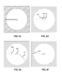
- FIG. 6a to 6h give different implementations of the blocking member.
- Figure 6a shows a square chip 600 of e.g. silicon with an outer edge 610.
- the outer edge is dimensioned such, that it can be contained in e.g. an aperture mechanism of the TEM, so that it can be positioned mechanically.
- a round hole 601 is etched with a diameter 608.
- the diameter of the hole is chosen such that electrons that are non-elastically deflected (and thus are scattered over a large angle or lost energy) are intercepted by the silicon.
- a support arm 606 Connected to the silicon 602 between the outer edge 610 and the outer diameter of the hole 601 is a support arm 606. At the distal end near the middle of the hole the support arm connect to the blocking member 604, that in this case is formed as a half circle.
- the half circle shows a straight edge, and the central beam of the diffraction pattern 612 is positioned close to this edge, but sufficiently removed that the blocking member does not intercept (much) of the electrons in the central beam.
- the radius of the half-circle is, for a high voltage of 300 kV, between for example 10-15 ⁇ m, although with other microscopes and other accelation voltages different values can be found.
- the support arm is preferable as thin as possible, and experiments resulted in a structure where the support arm had a width of 3 ⁇ m.
- the structure can be gilded, or otherwise plated with a highly conductive material to avoid charging.
- the substrate can be conductive, or insulating, according to the surface coating given. Both substrate material and coating can be changed to accommodate demands with respect to vacuum integrity, thermal behavior, machinability, etc.
- Figure 6B shows a similar chip with a rectangular blocking member.
- the blocking member not being semi-circular round the central beam implies that its working is not identical in all directions, and that the frequency where the SSB imaging blends into the 'normal' CFT behavior differs in those directions. This may lead to artifacts in that the lowest resolution (with a given contrast) visible in one direction differs from the lowest resolution visible in another direction.
- Figure 6C shows the blocking member of figure 6A , but now the support art is parallel to the straight edge of the half-circle.
- Figure 6D shows a blocking member with varying width.
- Figure 6E shows a blocking member 604 that is not only supported by support arm 606, as is the case in figure 6D , but also by a second support arm 630.
- the structure becomes much stiffer, resulting in, for example, a structure that is less prone to vibration.
- Figure 6F shows a structure where an insulator is used for the substrate, and the blocking member is electrically insulated of most of the chip.
- An electrical connection can be made at pad 640, whereby a current measurement can be made to determine how much current impinges on the blocking member.
- Variant with two or more electrical connection to the blocking member are envisaged, that may or may not use the other side of the structure as well.
- the blocking member on a thin, conductive foil that in itself is transparent to electrons.
Landscapes
- Chemical & Material Sciences (AREA)
- Analytical Chemistry (AREA)
- Analysing Materials By The Use Of Radiation (AREA)
Priority Applications (5)
| Application Number | Priority Date | Filing Date | Title |
|---|---|---|---|
| EP10167258A EP2400522A1 (fr) | 2010-06-24 | 2010-06-24 | Élément de blocage pour une utilisation dans le plan de diffraction d'un TEM |
| EP11171115.6A EP2400523B1 (fr) | 2010-06-24 | 2011-06-23 | Élément de blocage pour une utilisation dans le plan de diffraction d'un TEM |
| JP2011139664A JP5829842B2 (ja) | 2010-06-24 | 2011-06-23 | Temの回折平面における使用のためのブロッキング部材 |
| CN201110172913.8A CN102299037B (zh) | 2010-06-24 | 2011-06-24 | 在tem的衍射平面中使用的阻挡部件 |
| US13/168,415 US8637821B2 (en) | 2010-06-24 | 2011-06-24 | Blocking member for use in the diffraction plane of a TEM |
Applications Claiming Priority (1)
| Application Number | Priority Date | Filing Date | Title |
|---|---|---|---|
| EP10167258A EP2400522A1 (fr) | 2010-06-24 | 2010-06-24 | Élément de blocage pour une utilisation dans le plan de diffraction d'un TEM |
Publications (1)
| Publication Number | Publication Date |
|---|---|
| EP2400522A1 true EP2400522A1 (fr) | 2011-12-28 |
Family
ID=43231748
Family Applications (2)
| Application Number | Title | Priority Date | Filing Date |
|---|---|---|---|
| EP10167258A Withdrawn EP2400522A1 (fr) | 2010-06-24 | 2010-06-24 | Élément de blocage pour une utilisation dans le plan de diffraction d'un TEM |
| EP11171115.6A Not-in-force EP2400523B1 (fr) | 2010-06-24 | 2011-06-23 | Élément de blocage pour une utilisation dans le plan de diffraction d'un TEM |
Family Applications After (1)
| Application Number | Title | Priority Date | Filing Date |
|---|---|---|---|
| EP11171115.6A Not-in-force EP2400523B1 (fr) | 2010-06-24 | 2011-06-23 | Élément de blocage pour une utilisation dans le plan de diffraction d'un TEM |
Country Status (4)
| Country | Link |
|---|---|
| US (1) | US8637821B2 (fr) |
| EP (2) | EP2400522A1 (fr) |
| JP (1) | JP5829842B2 (fr) |
| CN (1) | CN102299037B (fr) |
Families Citing this family (9)
| Publication number | Priority date | Publication date | Assignee | Title |
|---|---|---|---|---|
| EP2485239A1 (fr) | 2011-02-07 | 2012-08-08 | FEI Company | Procédé de centrage d'un élément optique dans un TEM comprenant un élément d'amélioration du contraste |
| EP2624278B1 (fr) * | 2012-01-31 | 2014-07-30 | Hitachi High-Technologies Corporation | Plaque de phase |
| EP2667399A1 (fr) | 2012-05-23 | 2013-11-27 | FEI Company | Plaque de phase améliorée pour TEM |
| EP2704178B1 (fr) * | 2012-08-30 | 2014-08-20 | Fei Company | Imagerie d'un échantillon dans un TEM équipé d'une plaque de phase |
| JP6286270B2 (ja) | 2013-04-25 | 2018-02-28 | エフ イー アイ カンパニFei Company | 透過型電子顕微鏡内で位相版を用いる方法 |
| DE102013019297A1 (de) | 2013-11-19 | 2015-05-21 | Fei Company | Phasenplatte für ein Transmissionselektronenmikroskop |
| US12059560B2 (en) * | 2015-03-09 | 2024-08-13 | Centre National De La Recherche Scientifique | Method of forming a device comprising graphene |
| US9978557B2 (en) | 2016-04-21 | 2018-05-22 | Fei Company | System for orienting a sample using a diffraction pattern |
| DE102017106984B4 (de) | 2017-03-31 | 2022-02-10 | Carl Zeiss Microscopy Gmbh | Lichtmikroskop und Verfahren zum Betreiben eines Lichtmikroskops mit optimierter Beleuchtungsgeometrie |
Citations (5)
| Publication number | Priority date | Publication date | Assignee | Title |
|---|---|---|---|---|
| US5814815A (en) | 1995-12-27 | 1998-09-29 | Hitachi, Ltd. | Phase-contrast electron microscope and phase plate therefor |
| WO2003068399A2 (fr) * | 2002-02-18 | 2003-08-21 | MAX-PLANCK-Gesellschaft zur Förderung der Wissenschaften e.V. | Lame de phase pour la microscopie electronique et imagerie par microscopie electronique |
| US6674078B2 (en) | 2001-09-25 | 2004-01-06 | Jeol Ltd. | Differential contrast transmission electron microscope and method of processing data about electron microscope images |
| EP2131384A1 (fr) * | 2008-06-05 | 2009-12-09 | FEI Company | Plaque de phase hybride |
| DE102008037698A1 (de) * | 2008-08-14 | 2010-02-18 | Carl Zeiss Nts Gmbh | Elektronenmikroskop mit ringförmiger Beleuchtungsapertur |
Family Cites Families (2)
| Publication number | Priority date | Publication date | Assignee | Title |
|---|---|---|---|---|
| DE102007007923A1 (de) * | 2007-02-14 | 2008-08-21 | Carl Zeiss Nts Gmbh | Phasenschiebendes Element und Teilchenstrahlgerät mit phasenschiebenden Element |
| EP2091062A1 (fr) * | 2008-02-13 | 2009-08-19 | FEI Company | TEM avec correcteur d'aberrations et lame de phase |
-
2010
- 2010-06-24 EP EP10167258A patent/EP2400522A1/fr not_active Withdrawn
-
2011
- 2011-06-23 JP JP2011139664A patent/JP5829842B2/ja active Active
- 2011-06-23 EP EP11171115.6A patent/EP2400523B1/fr not_active Not-in-force
- 2011-06-24 US US13/168,415 patent/US8637821B2/en not_active Expired - Fee Related
- 2011-06-24 CN CN201110172913.8A patent/CN102299037B/zh active Active
Patent Citations (5)
| Publication number | Priority date | Publication date | Assignee | Title |
|---|---|---|---|---|
| US5814815A (en) | 1995-12-27 | 1998-09-29 | Hitachi, Ltd. | Phase-contrast electron microscope and phase plate therefor |
| US6674078B2 (en) | 2001-09-25 | 2004-01-06 | Jeol Ltd. | Differential contrast transmission electron microscope and method of processing data about electron microscope images |
| WO2003068399A2 (fr) * | 2002-02-18 | 2003-08-21 | MAX-PLANCK-Gesellschaft zur Förderung der Wissenschaften e.V. | Lame de phase pour la microscopie electronique et imagerie par microscopie electronique |
| EP2131384A1 (fr) * | 2008-06-05 | 2009-12-09 | FEI Company | Plaque de phase hybride |
| DE102008037698A1 (de) * | 2008-08-14 | 2010-02-18 | Carl Zeiss Nts Gmbh | Elektronenmikroskop mit ringförmiger Beleuchtungsapertur |
Non-Patent Citations (1)
| Title |
|---|
| K. DOWNING ET AL.: "Discrimination of heavy and light components in electron microscopy using single-sideband holographic techniques", OPTIK, vol. 42, 1975, pages 155 - 175 |
Also Published As
| Publication number | Publication date |
|---|---|
| JP2012009439A (ja) | 2012-01-12 |
| US20110315876A1 (en) | 2011-12-29 |
| EP2400523A1 (fr) | 2011-12-28 |
| CN102299037A (zh) | 2011-12-28 |
| CN102299037B (zh) | 2016-04-13 |
| JP5829842B2 (ja) | 2015-12-09 |
| EP2400523B1 (fr) | 2013-12-11 |
| US8637821B2 (en) | 2014-01-28 |
Similar Documents
| Publication | Publication Date | Title |
|---|---|---|
| EP2400523B1 (fr) | Élément de blocage pour une utilisation dans le plan de diffraction d'un TEM | |
| JP5388163B2 (ja) | 移相型の素子および移相型の素子を有する粒子ビーム装置 | |
| US8247782B2 (en) | Apparatus and method for investigating and/or modifying a sample | |
| JP6027942B2 (ja) | Tem用位相板 | |
| US9934936B2 (en) | Charged particle microscope with special aperture plate | |
| US8835846B2 (en) | Imaging a sample in a TEM equipped with a phase plate | |
| EP2131384B1 (fr) | Plaque de phase hybride | |
| EP1587128A1 (fr) | Dispositif et méthode d'inspection ou de modification d'une surface à l'aide d'un faisceau de particules chargées | |
| WO2014085406A1 (fr) | Microscope électronique à balayage pour imagerie inclinée | |
| JP2012164657A (ja) | コントラストを向上させる素子を具備するtemにおける光学素子をセンタリングするための方法 | |
| JP2016115680A (ja) | 収差補正開孔を有する走査型荷電粒子ビームデバイスおよびその動作方法 | |
| US7232997B2 (en) | Apparatus and method for investigating or modifying a surface with a beam of charged particles | |
| CN113466266A (zh) | 用于获取3d衍射数据的方法和系统 | |
| WO2011163397A1 (fr) | Ouverture de foucault passe-haut micro-usinée pour microscopie électronique | |
| JP5319579B2 (ja) | 位相差電子顕微鏡および位相板 | |
| JP2022071166A (ja) | 透過電子顕微鏡 | |
| KR20210113672A (ko) | 하전 입자 빔의 에너지 확산을 제어하는 장치 및 방법 | |
| Marko et al. | Requirements for phase-plate cryo-electron tomography |
Legal Events
| Date | Code | Title | Description |
|---|---|---|---|
| AK | Designated contracting states |
Kind code of ref document: A1 Designated state(s): AL AT BE BG CH CY CZ DE DK EE ES FI FR GB GR HR HU IE IS IT LI LT LU LV MC MK MT NL NO PL PT RO SE SI SK SM TR |
|
| AX | Request for extension of the european patent |
Extension state: BA ME RS |
|
| PUAI | Public reference made under article 153(3) epc to a published international application that has entered the european phase |
Free format text: ORIGINAL CODE: 0009012 |
|
| STAA | Information on the status of an ep patent application or granted ep patent |
Free format text: STATUS: THE APPLICATION IS DEEMED TO BE WITHDRAWN |
|
| 18D | Application deemed to be withdrawn |
Effective date: 20120629 |