EP0782172A2 - Systèmes de traitement par plasma - Google Patents
Systèmes de traitement par plasma Download PDFInfo
- Publication number
- EP0782172A2 EP0782172A2 EP96308504A EP96308504A EP0782172A2 EP 0782172 A2 EP0782172 A2 EP 0782172A2 EP 96308504 A EP96308504 A EP 96308504A EP 96308504 A EP96308504 A EP 96308504A EP 0782172 A2 EP0782172 A2 EP 0782172A2
- Authority
- EP
- European Patent Office
- Prior art keywords
- shield
- slot
- coil
- plasma processing
- processing system
- Prior art date
- Legal status (The legal status is an assumption and is not a legal conclusion. Google has not performed a legal analysis and makes no representation as to the accuracy of the status listed.)
- Withdrawn
Links
Images


Classifications
-
- H—ELECTRICITY
- H01—ELECTRIC ELEMENTS
- H01J—ELECTRIC DISCHARGE TUBES OR DISCHARGE LAMPS
- H01J37/00—Discharge tubes with provision for introducing objects or material to be exposed to the discharge, e.g. for the purpose of examination or processing thereof
- H01J37/32—Gas-filled discharge tubes
- H01J37/32431—Constructional details of the reactor
- H01J37/32458—Vessel
- H01J37/32477—Vessel characterised by the means for protecting vessels or internal parts, e.g. coatings
-
- H—ELECTRICITY
- H01—ELECTRIC ELEMENTS
- H01J—ELECTRIC DISCHARGE TUBES OR DISCHARGE LAMPS
- H01J37/00—Discharge tubes with provision for introducing objects or material to be exposed to the discharge, e.g. for the purpose of examination or processing thereof
- H01J37/32—Gas-filled discharge tubes
- H01J37/32009—Arrangements for generation of plasma specially adapted for examination or treatment of objects, e.g. plasma sources
- H01J37/32082—Radio frequency generated discharge
- H01J37/321—Radio frequency generated discharge the radio frequency energy being inductively coupled to the plasma
-
- Y—GENERAL TAGGING OF NEW TECHNOLOGICAL DEVELOPMENTS; GENERAL TAGGING OF CROSS-SECTIONAL TECHNOLOGIES SPANNING OVER SEVERAL SECTIONS OF THE IPC; TECHNICAL SUBJECTS COVERED BY FORMER USPC CROSS-REFERENCE ART COLLECTIONS [XRACs] AND DIGESTS
- Y10—TECHNICAL SUBJECTS COVERED BY FORMER USPC
- Y10S—TECHNICAL SUBJECTS COVERED BY FORMER USPC CROSS-REFERENCE ART COLLECTIONS [XRACs] AND DIGESTS
- Y10S156/00—Adhesive bonding and miscellaneous chemical manufacture
- Y10S156/916—Differential etching apparatus including chamber cleaning means or shield for preventing deposits
Definitions
- the invention relates to a system for depositing a conductive material onto a semiconductor wafer or other workpiece by high-density plasma deposition, and more particularly to an apparatus having a shield for preventing short circuiting of the system caused by formation of a continuous metal film on the inner walls of the apparatus.
- PVD Physical vapor deposition
- a coating of material is passed into a vapor transport phase by a physical mechanism, such as evaporation, sublimation or ion bombardment.
- Sputtering is one form of PVD wherein a material is dislodged and ejected from the surface of a solid or liquid due to the momentum exchange associated with surface bombardment by energetic particles.
- a source of coating material called the target is placed into a vacuum chamber along with a substrate, and the chamber is evacuated by a high vacuum and backfilled with a gas.
- This gas is partially ionized, and the ionized gas atoms are attracted to the target to physically eject particles of target material.
- the substrate is positioned in front of the target so that it intercepts a portion of the flux of sputtered atoms.
- the target particles are ejected in paths ranging from nearly parallel, to perpendicular to the target.
- many of the ejected particles will be travelling toward the substrate in non-perpendicular paths therewith. These particles can build up on the side wall of holes or trenches on the substrate, and block off the hole or trench before it is completely filled.
- a coil fed with R.F. power may be wound about a portion of the sputtering chamber to form a plasma consisting of a mixture of gas and charged atomic particles dislodged from the target.
- the atomic particles are attracted to the substrate upon application of an opposite charge to the substrate, which causes them to bombard the substrate in paths substantially perpendicular thereto.
- the coil should be placed within the vacuum chamber with minimal or no barrier between the coil and the gas to be ionized.
- exposing an RF field coil to the plasma and material being sputtered from the target can have several deleterious effects.
- each of the plasma and sputtered material causes a heat load on the RF field coil that must be removed.
- coil supports of RF feeds which are typically made of an insulating material, can get coated with sputtered material. If the sputtered material is a metal, this can create resistive current paths that can interfere with operation of the RF field coil, resulting in inconsistent coupling efficiency and inconsistent process characteristics.
- the RF field coil will become coated with sputtered material which flakes off during processing, which leads to process contamination or particle problems. Also, if high resistivity materials are being sputtered, such as Ti or TiN, there will be even higher resistive losses in the coil as it is coated.
- a containment vessel or shield assembly may be interdisposed between the coil and the gas, to shield the coil from the plasma yet still enable energy from the coil to reach the substrate. However, once conductive target material forms a continuous path around the interior surface of the shield, the coil will inductively couple into the conductive film, thereby extinguishing the plasma.
- the present invention solves these problems by providing a shield assembly for an RF field coil in a plasma processing system which protects the coil from the plasma and from bombardment with sputtered metal, and which also permits RF energy generated by the coil to pass through the shield assembly to couple with a plasma within the chamber.
- the invention is a plasma processing system including a vacuum chamber; an RF field coil surrounding a central space within the vacuum chamber, during plasma processing said RF coil coupling RF power into a plasma within the central space; and a coil shield assembly shielding the coil from the plasma.
- the coil shield assembly includes a first shield located inside the RF field coil, i.e., between the coil and the central space, and having at least one slot extending therethrough, and it includes a barrier structure positioned between the first shield and the coil and aligned with the at least one slot.
- the first shield and the barrier structure are structured and arranged to inhibit bridging of each slot by material deposited in the chamber during plasma processing.
- an inner surface of the barrier structure is spaced apart from the first shield proximal to the at least one slot, and positioned such that the surface of the barrier structure blocks all line-of-sight paths through the at least one slot between the central space and the coil.
- the at least one slot extends from a position proximate a top edge of the first shield to a position proximate a bottom edge of the first shield.
- the at least one slot is part of a plurality of slots circumferentially spaced around the first shield, and each of the slots of the plurality of slots has a shape which is a member of the group of shapes consisting of an I-shape, a straight line shape, and a herring bone-shape.
- the barrier structure includes a second shield having a plurality of slots circumferentially spaced around the second shield and extending therethrough, and the plurality of slots in the second shield are circumferentially offset from-the plurality of slots in the first shield, i.e., they are disposed at different radial paths from the center of the central space.
- At least one slot in the first shield extends completely through the first shield from top to bottom thereby splitting the first shield.
- the one slot in the first shield is a member of a plurality of circumferentially spaced slots which divide the first shield into individual segments which are electrically isolated from each other.
- the barrier structure includes a dielectric material and provides support to the first shield. The surface of the barrier structure includes a recess aligned with and proximate to the at least one slot of the first shield. Alternatively, the inner surface of the barrier structure is spaced apart from the first shield. Also in preferred embodiments, the barrier structure includes a second shield positioned between the first shield and the coil.
- the second shield includes at least one slot extending therethrough and which also extends from a position proximate a top edge of the second shield to a position proximate a bottom edge of the second shield.
- the at least one slot of the second shield is circumferentially offset from the at least one slot of the first shield.
- the coil shield assembly includes a dielectric wall positioned between the second shield and the coil. In some embodiments, the dielectric wall forms a wall of the chamber so that the coil is located outside of the chamber.
- the first and/or second shield may be removeably positioned within the chamber. Additionally, the section of the chamber which houses the RF coil and coil shield assembly of the present invention may be a separable extension from the remainder of the chamber.
- the at least one slot extends in a generally circumferential direction around the first shield.
- the RF field coil and the at least one slot are circumferentially and axially aligned at a plurality of circumferentially spaced crossing points at which the at least one slot is substantially transverse to the RF field coil.
- the RF field coil might be configured into a substantially rectangular-shaped pattern with the slot being substantially circular.
- the at least one slot might have a periodic rectangular-shaped pattern that is out of phase with the substantially rectangular-shaped pattern of the coil, or both the RF field coil and the slot could define substantially sawtooth-shaped patterns that are out of phase with each other.
- the invention is a plasma processing system for sputter depositing a material from a target onto a substrate.
- the plasma processing system includes a vacuum chamber; a platform which holds the substrate during plasma processing; a sputter source onto which the target is mounted; an RF coil located inside of the chamber and located between the target and the platform; and a coil shield assembly including a first shield located inside the RF coil and a barrier structure located between the first shield and the RF coil.
- the first shield includes at least one slot extending therethrough and the barrier structure is aligned with the at least one slot and spaced from the first shield proximal to the at least one slot such that there is no line of sight path from inside of the first shield to the RF coil.
- the invention is a plasma processing system including a chamber for containing a plasma; an RF field coil positioned outside the chamber; and a coil shield assembly.
- the coil shield assembly includes a dielectric wall forming a portion of a wall of the chamber inside the coil; and a first metallic shield inside the chamber, the first shield being split by a first slot extending in an axial direction, wherein the first shield is spaced apart from an inner surface of the dielectric wall near the first slot.
- the plasma processing system further includes a second metallic shield positioned between the dielectric wall and the first shield and spaced apart from the first shield.
- the second shield is split by a second slot that is circumferentially offset from the first slot in the first shield.
- the first slot is one of a first plurality of slots that divide the first shield into a first plurality of circumferentially spaced segments.
- the second slot is one of a second plurality of slots that divide the second shield into a second plurality of circumferentially spaced segments.
- each of the first plurality of slots is circumferentially offset from each of the second plurality of slots.
- the first and second shields are electrically isolated from each other and from ground.
- Fig. 1 shows a plasma processing system used for sputter depositing a film of material onto a substrate.
- Fig. 1 shows a plasma processing system used for sputter depositing a film of material onto a substrate.
- similar structures that are illustrated in different figures will be referred to by the same reference numbers.
- the plasma processing system includes a generally cylindrical chamber 10 having a first port 12 for evacuating chamber 10 with a pump 14 and a second port 16 for introducing process gas, such as, for example, argon, nitrogen, or reactive gases, from gas controls 18.
- a source assembly 20 at the top of chamber 10 has a sputter target 22 mounted thereto and facing downward into the interior of chamber 10.
- a movable platform 24 at the lower end of chamber 10 holds a substrate 26 onto which material sputtered from target 22 is deposited.
- Substrate 26 is typically a semiconductor wafer, however, the invention contemplates other types of substrates or other workpieces as well.
- a lift mechanism 28 moves platform 24 up and down, as illustrated by arrows in Fig. 1. After substrate 26 is placed on platform 24, lift mechanism 28 raises platform 24 until the outer perimeter of substrate contacts a clamping ring 30.
- a DC voltage power supply 32 coupled to target 22 provides power for initiating and sustaining a plasma deposition process During sputtering, power supply 32 typically biases target 22 to a negative voltage relative to an electrical ground. In many applications, a metal portion of wall 11 of chamber 10 is grounded. Source assembly 20 and target 22 are electrically isolated from chamber 10 by an insulator ring 33. In the embodiment illustrated, source assembly 20 includes a magnetron that has several magnets (not shown) positioned behind target 22 for improving sputtering efficiency. In such a system, which is well known in the art, source assembly 20 includes a mechanism for rotating the magnets around the back of target 22 to improve the uniformity of erosion of target material during sputtering.
- a system for coupling RF energy to a plasma generated by source assembly 20 is referenced generally by the numeral 15, and includes an RF field coil 34.
- Fig. 1 illustrates coil 34 located inside an evacuated space of chamber 10 and generally surrounding a central space 35 located between target 22 and substrate 26.
- RF field coil 34 has two leads 36 and 40. Lead 36 is connected to ground through a feed-through 38 in wall 11 and lead 40 is connected to an RF generating circuit 44 through a second feed-through 42 and via an RF coupling network 46.
- An insulating support ring 47 supports coil 34 within chamber 10.
- a coil shield assembly 48 is positioned generally inside RF field coil 34.
- Coil shield assembly 48 includes an inner shield 50 that is positioned close to, but separated from, RF field coil 34.
- Inner shield 50 may be metallic, or alternatively may be comprised of a non-conductive material such as ceramic or quartz.
- Inner shield 50 includes a plurality of evenly spaced slots 52 that are vertically aligned with the central axis of coil 34. Inner shield 50 prevents sputtered material from depositing onto coil 34 while slots 52 inhibit eddy currents in inner shield 50 that would attenuate the RF energy that penetrates into the central space 35 where it couples to the plasma.
- outer shield 54 is positioned between inner shield 50 and coil 34.
- Outer shield 54 has a surface 56 close to slots 52 but separated from inner shield 50 so that when sputtered material (e.g. metal) passing through slots 52 deposits onto surface 56, that material does not form an electrical short across the slot of inner shield 50 and eddy currents are thereby permitted to flow around inner shield 50.
- outer shield 54 is made of a dielectric material so that RF energy can pass through it into the central space 35 without being significantly attenuated.
- outer shield 54 also has vertical slots, which are circumferentially offset from slots 52 of inner shield 50, and may also be made of metal.
- the entire RF energy supply system 15 for chamber 10 may be configured within a separable extension 10b of the chamber 10.
- RF field coil 34 is embedded in outer shield 154.
- Outer shield 154 is preferably made of a dielectric material, and is attached to an insulating support 158 fastened to the wall 11 of chamber extension 10b.
- Chamber extension 10b attaches to and detaches from the stationary chamber 10a at point 13.
- Both the chamber wall extension 10b and the stationary chamber wall 10a are preferably formed of an insulating material such as ceramic or quartz.
- chamber extension 10b facilitates servicing and cleaning of the individual components of the system.
- This alternative configuration enables an existing standard sputtering chamber to be conveniently converted into an inductively coupled sputtering chamber, by the placement of such a chamber extension 10b having an RF energy supply system 15 as presently described, between a standard sputter chamber and a source assembly.
- RF field coil 34 may be supported between insulating support 158, being generally tubular-shaped and having a diameter larger than RF field coil 34, and the outer shield 154, positioned radially inside the RF field coil 34.
- RF field coil 34 may be supported within grooves 160 formed in surfaces of one or both of support 158 and outer shield 154.
- Support 158 is fastened to chamber wall 11 such that RF field coil 34 is electrically isolated from the grounded chamber.
- Inner shield 150 which may be metallic and which may include a plurality of slots 152, is mounted on an inner surface of outer shield 154 by fasteners 162 that also secure outer shield 154 to insulating support 158. Slots 152 extend completely through inner shield 150 from top to bottom such that inner shield 150 is divided into a plurality of discrete segments. The segments are electrically isolated from ground and from each other. Thus, there are no closed loop current paths around the inner shield 150 or between segments of the shield over which the RF field can induce eddy currents that reduce the coupling of the RF signal to the plasma within central region 35 inside inner shield 150.
- Outer shield 154 being a dielectric or insulator material, is transparent to the RF signal generated by coil 34.
- Inner shield 150 protects an inner surface 156 of outer shield 154 from sputtered material from the target, except for a plurality of strips located behind slots 152.
- recesses 164 or grooves are formed in surface 156 behind each slot 152.
- Each recess 164 is aligned with a corresponding slot in inner shield 150 and is wider than the width of its corresponding slot. In other words, each recess 164 is wide enough circumferentially such that material deposited within recess 164 will not short the inner shield segments together.
- Figure 3b illustrates an alternative embodiment of the coil shield assembly of the present invention, wherein the outer shield and inner shield are integrated to form a single shield 153 of a non-conductive material.
- the slots 164 formed within shield 153 are preferably T-shaped, such that formation of a continuous film of material deposited on the inner surface of the shield is prevented.
- metallic top shield 68 overhangs an upper portion of inner shield 150 near target 22, and provides shielding of both an upper portion of inner shield 150 located closest to target 22 and the tubular-shaped support 158 to prevent them from being coated with sputtered material from target 22.
- Top shield 68 is electrically coupled to a grounded wall of chamber 10.
- a lower portion of inner shield 150 located near platform 24 is radially spaced between two vertically extending portions of a metallic bottom shield 70.
- Bottom shield 70 extends below inner shield 150 and shields a lower portion of chamber 10 near the movable platform 24 from bombardment with sputtered material.
- a central opening 72 in bottom shield allows platform 24 to be raised up into process position where the substrate contacts clamping ring 30 in the preferred embodiment.
- Bottom shield 70 is supported by a hangar 74 that is electrically coupled to the grounded wall 11 of chamber 10.
- Top shield 68 and bottom shield 70 are each grounded so as to provide a return path for a DC current from sputtered ions. Top and bottom shields 68 and 70 also protect tubular-shaped support 158 and outer shield 154 from heat produced by the plasma and from bombardment by sputtered material.
- Metallic inner shield 150 floats electrically, with each segment isolated from the other segments so as not to provide a path for eddy currents to circulate around the circumference of inner shield 150 or around the slots 152.
- inner shield 150 may also be removable with respect to a fixed outer shield 154 and coil 34 to facilitate cleaning or servicing of the shield 150 and shield assembly 48.
- an alternative embodiment of a coil shield assembly 48 includes a slotted, metallic outer shield 254 interposed between and separated from each of inner shield 250 and coil 34.
- Outer shield 254 has a plurality of slots 276 that are circumferentially offset from an equal number of slots 252 in inner shield 250 such that there are no direct, line-of-sight paths between central space 35 and coil 34.
- Inner shield 250 and outer shield 254 are electrically isolated from each other and from ground.
- slots 252 pass completely through inner shield 250 from top to bottom so as to divide inner shield 250 into discrete, electrically isolated segments.
- slots 276 pass completely through outer shield 254 from top to bottom and divide outer shield 254 into discrete, electrically isolated segments.
- Coil 34 is supported in a generally tubular-shaped, insulating support 258 by, for example, projections (not shown) extending radially inward from insulating support 258.
- each segment of inner shield 250 there is one or more radially extending tabs 251 that rest on insulating support 258 so as to hold that segment of inner shield 250 in place within chamber 10.
- at an upper end of each segment of outer shield 254 there is one or more radially extending tabs 255 which hang on insulating support 258 to keep that outer shield segment in place.
- Tabs 251 and 255 are alternately positioned on insulating support 258 and electrically isolated from each other. Fasteners and insulating spacers or bushings (not shown) can be used to secure the segments of the inner and outer shields 250 and 254 onto support 258.
- Fig. 4a shows only four slots 252 in inner shield 250 and four slots 276 in outer shield 254. It should be understood, however, that this is not meant to be limiting and that in practice there could be more slots or there even could be fewer slots.
- arrows in Fig. 4a indicate projections of straight, line-of-sight paths that sputtered material or plasma ions may travel from central space 35 through one of slots 252.
- Slots 276 in outer shield 254 are sufficiently offset from slots 252 in inner shield 250 so that there is no line of sight path through the slots in both shield to coil 34. As indicated above, this prevents sputtered material and ions from reaching and depositing onto coil 34 during processing.
- Fig. 4 does not include an insulating support positioned between coil 34 and outer shield 254 and supporting outer shield 254.
- that type of arrangement is also contemplated as being within the scope of the invention.
- coil 34 is positioned within chamber 10. Coil 34 is not a perfect conductor of RF power and it will exhibit some losses which generate heat. To facilitate removal of this heat, coil 34 is made from metal tubing (e.g. copper), and water or some other coolant is circulated through the coil during plasma processing.
- metal tubing e.g. copper
- coil 34 of coil shield assembly 48 is located outside of chamber 10. In this configuration, convection cooling of coil 34 by the surrounding air will often be sufficient to cool coil 34 and thus the problems inherent in attempting to pass livid to the coil through the chamber are prevented.
- a cylindrically-shaped outer support 358 is positioned radially outside coil 34 and is structured to support coil 34, for example, with inwardly extending pegs (not shown) or other suitable means.
- Another cylindrically-shaped inner support 359 is positioned radially inside coil 34 and functions as the outer wall of the vacuum chamber. Both outer support 358 and inner support 359 are made of a dielectric material (e.g. ceramic or quartz). O-rings 378, 380 and 382 form vacuum seals where the inner and outer supports 359 and 358 mate with other chamber components.
- An inner shield 350 and an outer shield 354, both of which may be made of metal or another conductor, are positioned as closely as possible to inner support 359 and thus to coil 34.
- Outer shield 354 is positioned between insulating inner support 359 and inner shield 350, but without electrically contacting inner shield 350.
- a plurality of slots 352 extending through inner shield from top to bottom divide inner shield 350 into discrete, electrically isolated segments.
- a plurality of slots 376 circumferentially offset from slots 352 similarly divide outer shield 354 into discrete, electrically isolated segments. Shields 350 and 354 and their respective slots 352 and 376 are aligned such that there are no direct, line-of-sight paths between central space 35 and inner support 359.
- shields 350 and 354 are electrically isolated from each other and from ground.
- the segments of each shield 350 and 354 are each supported by tabs 351 and 355 which rest on the inner insulating support 359 in a manner similar to that described above in connection with Fig. 4a.
- Fasteners and insulating spacers can be used to secure each segment of inner and outer shields to support 359.
- an alternative embodiment of a coil shield assembly 48 includes RF field coil 34 located within chamber 10.
- Structure for supporting RF coil 34 can be provided, for example, by a cylindrically-shaped, insulating support 458 having pegs (not shown) or other inwardly projecting structures holding the turns of coil 34.
- An inner shield 450 is positioned inside coil 34 and includes a plurality of slots 452 spaced evenly around the circumference of shield 450. In this embodiment, slots 452 pass through inner shield 450 however do not extend entirely from top to bottom of shield 450. Each slot 452 extends from a position just below a top edge the top of inner shield 450 to a position just above a lower end 486 of inner shield 450.
- a metallic outer shield 454 is positioned between inner shield 450 and coil 34 and is radially spaced apart from each.
- Outer shield 454 contains a plurality of evenly spaced apart, open slots 456 that are circumferentially offset from slots 452 of inner shield 450 so that there are no line-of sight paths from central space 35 to coil 34.
- Both inner shield 450 and outer shield 454 may be made of metal.
- both inner shield 450 and outer shield 454 are grounded.
- each of inner shield 450 and outer shield 454 includes an outwardly extending lip at their upper ends, indicated in the drawing with reference characters 451 and 455, respectively, for supporting and attaching them to chamber 10. Since inner shield 450 is grounded it forms part of the return path for the sputter current.
- a bottom shield 70 is also provided to protect the bottom components of chamber 10 from being exposed to the sputtered material.
- Slots 452 and 456 allow RF energy generated by RF field coil 34 to penetrate into central region 35 to produce a plasma.
- Inner and outer shields 450 and 454 protect coil 34 from the plasma, and block out direct deposition of material sputtered from target 22 onto coil 34.
- Fig. 6 shows slots 452 and 456 that are straight and vertically oriented (i.e., oriented parallel to the central axis of the chamber 10), other configurations are contemplated within the scope of the invention.
- Some other slot shapes that provide possibly better suppression of eddy currents in the metal shields include I-shaped slots 552 (Fig. 7a), herringbone-shaped slots 652 (Fig. 7b), and slanted line-shaped slots 752 (Fig. 7c). These more complexly shaped slots increase the length of the path over which the eddy currents must flow and thereby increase the resistance as seen by such currents.
- FIG. 8a another type of a slotted coil shield assembly includes a shield that has a circumferentially extending slot.
- the slot and RF field coil are each structured and arranged such that they are oriented substantially transverse to each other at circumferentially and axially aligned crossing points.
- a single-turn RF field coil 834 is shaped in a repeating rectangular manner with circumferentially oriented coil portions 842 and 844 connected by axially extending coil portions 846.
- Shield 850 forms a circular slot 852 that divides shield 850 into two segments.
- Coil 834 is positioned relative to circular slot 852 so that slot 852 is approximately mid-way between the coil portions 842 and 844.
- a radial projection of circular slot 852 onto coil 834 intersects only axial portions 846.
- Fig. 8b illustrates a coil shield assembly in which both an RF field coil 934 and a generally circumferentially extending slot 952 in a shield 950 are shaped in a repeating rectangular manner.
- the rectangular pattern of slot 952 has a larger amplitude than the rectangular pattern of coil 934.
- coil 935 and slot 952 are circumferentially offset from each other by about a quarter of a period so that if the pattern of slot 952 is projected onto coil 934, it intersects only circumferential portions 980 and 982 of coil 934.
- Fig. 8c illustrates a coil shield assembly in which each of an RF field coil 1034 and a slot 1052 in a shield 1050 are sawtooth-shaped. and offset from each other by about a quarter of a period. Thus, a radial projection of slot 1052 onto coil 1034 intersects coil 1034 at the midway point of each linear portion of its saw-tooth pattern.
- a barrier or outer shield, can be interposed between the RF field coil and the shield.
- the barrier can be, for example, an insulating tube or a slotted metallic tube. It is also understood that the RF field coil may be embedded in the outer shield as previously described with reference to Figure 2.
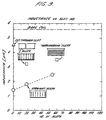
- FIG. 9 shows the results of our experiments.
- slots of more elaborate designs e.g. I-shaped slots or herringbone-shaped slots
- improves coupling the greatest improvement, however, occurs by extending the slot so that it cuts entirely through the shield from top to bottom. Note that our measurements indicated that a shield with just a single "full cut” slot performed better than any of the designs in which there were multiple slots none of which passed all of the way through the shield from top to bottom.
- the slots In designing a coil shield assembly, two criteria are balanced in determining the width of the slots. First, the slots should be narrow enough so that there is no substantial plasma leakage through the slots. Second, the slots should be wide enough such that they will not be bridged by sputtered metal. A slot width of approximately 0.06 inches or greater is generally sufficient to prevent bridging occurring more often than one or more cleaning cycles of a process system.
- the slots for the outer shield can be narrower since these slots are not exposed to sputtered material.
- the inner shield and outer shield should also be radially spaced so as to prevent the formation of a bridging material layer between the two shields during use. It is also apparent that the inner and/or outer shields of the present invention may be conveniently removeably positioned within the chamber.
- An additional design consideration is the spacing between the metallic shields and the coil. In general, it is desirable to position the coil as close as possible to the inner metallic shield so as to achieve the maximum coupling to the plasma within the chamber.
- the metallic shields can be made of any type of metal compatible with the process undertaken in the chamber. In choosing a material, one may consider the material being sputter deposited and choose a shield material that the sputtered material will adhere to such as to inhibit contamination of the chamber by flaking. One may also want to choose a shield material that is compatible with a chemical process to remove the sputtered on material so that the shields can be re-used. These factors are generally known to those of ordinary skill in the art.
- the RF field coil can be just a single winding or it can have multiple windings.
- the number of windings will generally be a compromise between power loss and impedance matching, and will therefore depend upon the RF frequency of operation.
Landscapes
- Physics & Mathematics (AREA)
- Engineering & Computer Science (AREA)
- Plasma & Fusion (AREA)
- Chemical & Material Sciences (AREA)
- Analytical Chemistry (AREA)
- Plasma Technology (AREA)
- Physical Vapour Deposition (AREA)
Applications Claiming Priority (4)
| Application Number | Priority Date | Filing Date | Title |
|---|---|---|---|
| US56316695A | 1995-11-27 | 1995-11-27 | |
| US563166 | 1995-11-27 | ||
| US08/676,599 US5763851A (en) | 1995-11-27 | 1996-07-03 | Slotted RF coil shield for plasma deposition system |
| US676599 | 1996-07-03 |
Publications (2)
| Publication Number | Publication Date |
|---|---|
| EP0782172A2 true EP0782172A2 (fr) | 1997-07-02 |
| EP0782172A3 EP0782172A3 (fr) | 1997-10-08 |
Family
ID=27073190
Family Applications (1)
| Application Number | Title | Priority Date | Filing Date |
|---|---|---|---|
| EP96308504A Withdrawn EP0782172A3 (fr) | 1995-11-27 | 1996-11-25 | Systèmes de traitement par plasma |
Country Status (3)
| Country | Link |
|---|---|
| US (1) | US5763851A (fr) |
| EP (1) | EP0782172A3 (fr) |
| KR (1) | KR970030287A (fr) |
Cited By (29)
| Publication number | Priority date | Publication date | Assignee | Title |
|---|---|---|---|---|
| EP0827183A1 (fr) * | 1996-08-30 | 1998-03-04 | Galvano-T electroforming-plating GmbH | Conteneur sous vide, perméable à la RF, avec écran Faraday intégré |
| EP0845151A1 (fr) * | 1996-05-09 | 1998-06-03 | Applied Materials, Inc. | Bobinage a evidement servant a generer un plasma |
| WO1998048444A1 (fr) | 1997-04-21 | 1998-10-29 | Tokyo Electron Arizona, Inc. | Procede et dispositif de pulverisation par bombardement ionique sur un materiau |
| WO1999003313A1 (fr) * | 1997-07-09 | 1999-01-21 | Surface Technology Systems Limited | Appareil de traitement au plasma |
| WO1999014791A1 (fr) * | 1997-09-15 | 1999-03-25 | Applied Materials, Inc. | Dispositif permettant de pulveriser un materiau ionise dans un plasma de densite moyenne a elevee |
| WO1999014790A1 (fr) * | 1997-09-16 | 1999-03-25 | Applied Materials, Inc. | Chauffage par resistance d'une bobine de puissance visant a reduire les effets du chauffage/demarrage transitoires |
| EP0818803A3 (fr) * | 1996-07-10 | 1999-03-31 | Applied Materials, Inc. | Ecran électriquement flottant dans un réacteur à plasma |
| EP0908922A1 (fr) * | 1997-10-10 | 1999-04-14 | European Community | Chambre de traitement par plasma et dispositif utilisant cette chambre de traitement |
| US5948215A (en) * | 1997-04-21 | 1999-09-07 | Tokyo Electron Limited | Method and apparatus for ionized sputtering |
| EP0841683A3 (fr) * | 1996-10-08 | 1999-12-01 | Applied Materials, Inc. | Ecran actif de génération d'un plasma pour la pulvérisation |
| WO1999066531A1 (fr) * | 1998-06-16 | 1999-12-23 | Surface Technology Systems Limited | Appareil de traitement par plasma |
| WO2000003055A1 (fr) * | 1998-07-13 | 2000-01-20 | Tokyo Electron Arizona, Inc. | Ecran pour appareil de depot physique en phase vapeur ionisee |
| WO2000019483A1 (fr) * | 1998-09-30 | 2000-04-06 | Unaxis Balzers Aktiengesellschaft | Chambre de traitement sous vide et procede de traitement de surface |
| US6080287A (en) * | 1998-05-06 | 2000-06-27 | Tokyo Electron Limited | Method and apparatus for ionized physical vapor deposition |
| US6132566A (en) * | 1998-07-30 | 2000-10-17 | Applied Materials, Inc. | Apparatus and method for sputtering ionized material in a plasma |
| US6190513B1 (en) | 1997-05-14 | 2001-02-20 | Applied Materials, Inc. | Darkspace shield for improved RF transmission in inductively coupled plasma sources for sputter deposition |
| US6197165B1 (en) | 1998-05-06 | 2001-03-06 | Tokyo Electron Limited | Method and apparatus for ionized physical vapor deposition |
| US6237526B1 (en) | 1999-03-26 | 2001-05-29 | Tokyo Electron Limited | Process apparatus and method for improving plasma distribution and performance in an inductively coupled plasma |
| US6254746B1 (en) | 1996-05-09 | 2001-07-03 | Applied Materials, Inc. | Recessed coil for generating a plasma |
| US6287435B1 (en) | 1998-05-06 | 2001-09-11 | Tokyo Electron Limited | Method and apparatus for ionized physical vapor deposition |
| WO2000079568A3 (fr) * | 1999-06-18 | 2001-11-15 | Applied Materials Inc | Reacteur au plasma muni de multiples petites antennes inductives internes |
| US6345588B1 (en) | 1997-08-07 | 2002-02-12 | Applied Materials, Inc. | Use of variable RF generator to control coil voltage distribution |
| US6474258B2 (en) | 1999-03-26 | 2002-11-05 | Tokyo Electron Limited | Apparatus and method for improving plasma distribution and performance in an inductively coupled plasma |
| US6494998B1 (en) | 2000-08-30 | 2002-12-17 | Tokyo Electron Limited | Process apparatus and method for improving plasma distribution and performance in an inductively coupled plasma using an internal inductive element |
| US6579426B1 (en) | 1997-05-16 | 2003-06-17 | Applied Materials, Inc. | Use of variable impedance to control coil sputter distribution |
| WO2006083332A1 (fr) * | 2004-10-05 | 2006-08-10 | Applied Materials, Inc. | Appareil pour depot en phase vapeur par plasma metallique et repulverisation avec frequences de puissance source et de polarisation appliquees par le biais de la piece a travailler |
| US7214619B2 (en) | 2004-10-05 | 2007-05-08 | Applied Materials, Inc. | Method for forming a barrier layer in an integrated circuit in a plasma with source and bias power frequencies applied through the workpiece |
| US7244344B2 (en) | 2005-02-03 | 2007-07-17 | Applied Materials, Inc. | Physical vapor deposition plasma reactor with VHF source power applied through the workpiece |
| CN107301943A (zh) * | 2017-07-27 | 2017-10-27 | 北京北方华创微电子装备有限公司 | 法拉第屏蔽件及反应腔室 |
Families Citing this family (53)
| Publication number | Priority date | Publication date | Assignee | Title |
|---|---|---|---|---|
| US6224724B1 (en) * | 1995-02-23 | 2001-05-01 | Tokyo Electron Limited | Physical vapor processing of a surface with non-uniformity compensation |
| US6264812B1 (en) | 1995-11-15 | 2001-07-24 | Applied Materials, Inc. | Method and apparatus for generating a plasma |
| KR100489918B1 (ko) * | 1996-05-09 | 2005-08-04 | 어플라이드 머티어리얼스, 인코포레이티드 | 플라즈마발생및스퍼터링용코일 |
| JP3640478B2 (ja) * | 1996-09-20 | 2005-04-20 | アネルバ株式会社 | プラズマ処理装置 |
| US6254737B1 (en) | 1996-10-08 | 2001-07-03 | Applied Materials, Inc. | Active shield for generating a plasma for sputtering |
| JPH10172792A (ja) * | 1996-12-05 | 1998-06-26 | Tokyo Electron Ltd | プラズマ処理装置 |
| JP3846970B2 (ja) * | 1997-04-14 | 2006-11-15 | キヤノンアネルバ株式会社 | イオン化スパッタリング装置 |
| US6210539B1 (en) | 1997-05-14 | 2001-04-03 | Applied Materials, Inc. | Method and apparatus for producing a uniform density plasma above a substrate |
| US6077402A (en) * | 1997-05-16 | 2000-06-20 | Applied Materials, Inc. | Central coil design for ionized metal plasma deposition |
| US6361661B2 (en) * | 1997-05-16 | 2002-03-26 | Applies Materials, Inc. | Hybrid coil design for ionized deposition |
| US6071372A (en) | 1997-06-05 | 2000-06-06 | Applied Materials, Inc. | RF plasma etch reactor with internal inductive coil antenna and electrically conductive chamber walls |
| US20060137821A1 (en) * | 2004-12-28 | 2006-06-29 | Lam Research Coporation | Window protector for sputter etching of metal layers |
| EP0951049A1 (fr) * | 1998-04-16 | 1999-10-20 | Balzers Aktiengesellschaft | Baque de retenue, cible et son procédé de fabrication |
| US6146508A (en) * | 1998-04-22 | 2000-11-14 | Applied Materials, Inc. | Sputtering method and apparatus with small diameter RF coil |
| US6217718B1 (en) | 1999-02-17 | 2001-04-17 | Applied Materials, Inc. | Method and apparatus for reducing plasma nonuniformity across the surface of a substrate in apparatus for producing an ionized metal plasma |
| US6254745B1 (en) * | 1999-02-19 | 2001-07-03 | Tokyo Electron Limited | Ionized physical vapor deposition method and apparatus with magnetic bucket and concentric plasma and material source |
| US6168696B1 (en) | 1999-09-01 | 2001-01-02 | Micron Technology, Inc. | Non-knurled induction coil for ionized metal deposition, sputtering apparatus including same, and method of constructing the apparatus |
| EP1102305B1 (fr) * | 1999-11-17 | 2003-05-07 | European Community (EC) | Appareil de traitement par plasma avec paroi électriquement conductrice |
| TW584905B (en) | 2000-02-25 | 2004-04-21 | Tokyo Electron Ltd | Method and apparatus for depositing films |
| US6743340B2 (en) * | 2002-02-05 | 2004-06-01 | Applied Materials, Inc. | Sputtering of aligned magnetic materials and magnetic dipole ring used therefor |
| US6946054B2 (en) | 2002-02-22 | 2005-09-20 | Tokyo Electron Limited | Modified transfer function deposition baffles and high density plasma ignition therewith in semiconductor processing |
| US7176469B2 (en) * | 2002-05-22 | 2007-02-13 | The Regents Of The University Of California | Negative ion source with external RF antenna |
| US20040129221A1 (en) * | 2003-01-08 | 2004-07-08 | Jozef Brcka | Cooled deposition baffle in high density plasma semiconductor processing |
| KR101001743B1 (ko) * | 2003-11-17 | 2010-12-15 | 삼성전자주식회사 | 헬리컬 자기-공진 코일을 이용한 이온화 물리적 기상 증착장치 |
| US7713390B2 (en) * | 2005-05-16 | 2010-05-11 | Applied Materials, Inc. | Ground shield for a PVD chamber |
| US8617672B2 (en) | 2005-07-13 | 2013-12-31 | Applied Materials, Inc. | Localized surface annealing of components for substrate processing chambers |
| US7811411B2 (en) * | 2005-08-09 | 2010-10-12 | Applied Materials, Inc. | Thermal management of inductively coupled plasma reactors |
| US8356575B2 (en) * | 2005-09-09 | 2013-01-22 | Ulvac, Inc. | Ion source and plasma processing apparatus |
| US20070074968A1 (en) * | 2005-09-30 | 2007-04-05 | Mirko Vukovic | ICP source for iPVD for uniform plasma in combination high pressure deposition and low pressure etch process |
| US20070113783A1 (en) * | 2005-11-19 | 2007-05-24 | Applied Materials, Inc. | Band shield for substrate processing chamber |
| US7685965B1 (en) * | 2006-01-26 | 2010-03-30 | Lam Research Corporation | Apparatus for shielding process chamber port |
| US7591232B2 (en) * | 2006-03-31 | 2009-09-22 | Tokyo Electron Limited | Internal coil with segmented shield and inductively-coupled plasma source and processing system therewith |
| US7879184B2 (en) * | 2006-06-20 | 2011-02-01 | Lam Research Corporation | Apparatuses, systems and methods for rapid cleaning of plasma confinement rings with minimal erosion of other chamber parts |
| US7959775B2 (en) * | 2006-09-29 | 2011-06-14 | Tokyo Electron Limited | Thermal stress-failure-resistant dielectric windows in vacuum processing systems |
| US7981262B2 (en) | 2007-01-29 | 2011-07-19 | Applied Materials, Inc. | Process kit for substrate processing chamber |
| US8980049B2 (en) * | 2007-04-02 | 2015-03-17 | Charm Engineering Co., Ltd. | Apparatus for supporting substrate and plasma etching apparatus having the same |
| US7942969B2 (en) | 2007-05-30 | 2011-05-17 | Applied Materials, Inc. | Substrate cleaning chamber and components |
| US20090056877A1 (en) | 2007-08-31 | 2009-03-05 | Tokyo Electron Limited | Plasma processing apparatus |
| JP2010001565A (ja) * | 2008-05-20 | 2010-01-07 | Canon Anelva Corp | スパッタリング装置、それを用いた太陽電池及び画像表示装置の製造方法 |
| JP5099101B2 (ja) * | 2009-01-23 | 2012-12-12 | 東京エレクトロン株式会社 | プラズマ処理装置 |
| US9462670B2 (en) * | 2010-07-16 | 2016-10-04 | Hypertherm, Inc. | Diffuser shape vent slots in a hand torch shield castellation |
| TWI502617B (zh) * | 2010-07-21 | 2015-10-01 | 應用材料股份有限公司 | 用於調整電偏斜的方法、電漿處理裝置與襯管組件 |
| WO2012040986A1 (fr) * | 2010-09-27 | 2012-04-05 | 北京北方微电子基地设备工艺研究中心有限责任公司 | Appareil de traitement par plasma |
| TW201328437A (zh) * | 2011-12-22 | 2013-07-01 | Atomic Energy Council | 具移動式磁鐵機構之電漿火炬裝置 |
| US8647485B2 (en) | 2012-03-30 | 2014-02-11 | Applied Materials, Inc. | Process kit shield for plasma enhanced processing chamber |
| US10512553B2 (en) * | 2014-07-30 | 2019-12-24 | The Alfred E. Mann Foundation For Scientific Research | Inductive link coil de-tuning compensation and control |
| US11037765B2 (en) * | 2018-07-03 | 2021-06-15 | Tokyo Electron Limited | Resonant structure for electron cyclotron resonant (ECR) plasma ionization |
| KR102473872B1 (ko) * | 2018-11-02 | 2022-12-06 | 베이징 나우라 마이크로일렉트로닉스 이큅먼트 씨오., 엘티디. | 라이닝 어셈블리, 반응 챔버 및 반도체 가공 디바이스 |
| US12077850B2 (en) * | 2021-08-05 | 2024-09-03 | Taiwan Semiconductor Manufacturing Company Ltd. | Physical vapor deposition apparatus |
| US20240395449A1 (en) * | 2021-09-20 | 2024-11-28 | Lam Research Corporation | Enclosure for mitigating rf power ramp up in icp source |
| CN113903649B (zh) * | 2021-09-23 | 2024-04-12 | 北京北方华创微电子装备有限公司 | 半导体工艺设备 |
| KR20230056817A (ko) * | 2021-10-20 | 2023-04-28 | 세메스 주식회사 | 안테나 부재 및 기판 처리 장치 |
| CN121726305B (zh) * | 2026-02-13 | 2026-04-21 | 上海邦芯半导体科技有限公司 | 一种反应腔体及等离子体处理设备 |
Family Cites Families (9)
| Publication number | Priority date | Publication date | Assignee | Title |
|---|---|---|---|---|
| US4304983A (en) * | 1980-06-26 | 1981-12-08 | Rca Corporation | Plasma etching device and process |
| US4886160A (en) * | 1988-11-07 | 1989-12-12 | Kligerman Alan E | Carton for containing a plurality of items for transport, storage and display |
| JPH07123121B2 (ja) * | 1986-09-24 | 1995-12-25 | 松下電器産業株式会社 | プラズマ処理装置 |
| US5302343A (en) * | 1987-02-25 | 1994-04-12 | Adir Jacob | Process for dry sterilization of medical devices and materials |
| US5234529A (en) * | 1991-10-10 | 1993-08-10 | Johnson Wayne L | Plasma generating apparatus employing capacitive shielding and process for using such apparatus |
| US5231334A (en) * | 1992-04-15 | 1993-07-27 | Texas Instruments Incorporated | Plasma source and method of manufacturing |
| DE4241927C2 (de) * | 1992-12-11 | 1994-09-22 | Max Planck Gesellschaft | Zur Anordnung in einem Vakuumgefäß geeignete selbsttragende isolierte Elektrodenanordnung, insbesondere Antennenspule für einen Hochfrequenz-Plasmagenerator |
| JPH07153748A (ja) * | 1993-11-29 | 1995-06-16 | M C Electron Kk | 灰化処理装置 |
| US5540800A (en) * | 1994-06-23 | 1996-07-30 | Applied Materials, Inc. | Inductively coupled high density plasma reactor for plasma assisted materials processing |
-
1996
- 1996-07-03 US US08/676,599 patent/US5763851A/en not_active Expired - Fee Related
- 1996-11-22 KR KR1019960056400A patent/KR970030287A/ko not_active Ceased
- 1996-11-25 EP EP96308504A patent/EP0782172A3/fr not_active Withdrawn
Non-Patent Citations (1)
| Title |
|---|
| None |
Cited By (44)
| Publication number | Priority date | Publication date | Assignee | Title |
|---|---|---|---|---|
| EP0845151A1 (fr) * | 1996-05-09 | 1998-06-03 | Applied Materials, Inc. | Bobinage a evidement servant a generer un plasma |
| US6254746B1 (en) | 1996-05-09 | 2001-07-03 | Applied Materials, Inc. | Recessed coil for generating a plasma |
| EP0818803A3 (fr) * | 1996-07-10 | 1999-03-31 | Applied Materials, Inc. | Ecran électriquement flottant dans un réacteur à plasma |
| EP0827183A1 (fr) * | 1996-08-30 | 1998-03-04 | Galvano-T electroforming-plating GmbH | Conteneur sous vide, perméable à la RF, avec écran Faraday intégré |
| EP0841683A3 (fr) * | 1996-10-08 | 1999-12-01 | Applied Materials, Inc. | Ecran actif de génération d'un plasma pour la pulvérisation |
| WO1998048444A1 (fr) | 1997-04-21 | 1998-10-29 | Tokyo Electron Arizona, Inc. | Procede et dispositif de pulverisation par bombardement ionique sur un materiau |
| US5948215A (en) * | 1997-04-21 | 1999-09-07 | Tokyo Electron Limited | Method and apparatus for ionized sputtering |
| US6190513B1 (en) | 1997-05-14 | 2001-02-20 | Applied Materials, Inc. | Darkspace shield for improved RF transmission in inductively coupled plasma sources for sputter deposition |
| US6579426B1 (en) | 1997-05-16 | 2003-06-17 | Applied Materials, Inc. | Use of variable impedance to control coil sputter distribution |
| WO1999003313A1 (fr) * | 1997-07-09 | 1999-01-21 | Surface Technology Systems Limited | Appareil de traitement au plasma |
| US6345588B1 (en) | 1997-08-07 | 2002-02-12 | Applied Materials, Inc. | Use of variable RF generator to control coil voltage distribution |
| WO1999014791A1 (fr) * | 1997-09-15 | 1999-03-25 | Applied Materials, Inc. | Dispositif permettant de pulveriser un materiau ionise dans un plasma de densite moyenne a elevee |
| US6565717B1 (en) | 1997-09-15 | 2003-05-20 | Applied Materials, Inc. | Apparatus for sputtering ionized material in a medium to high density plasma |
| US6023038A (en) * | 1997-09-16 | 2000-02-08 | Applied Materials, Inc. | Resistive heating of powered coil to reduce transient heating/start up effects multiple loadlock system |
| WO1999014790A1 (fr) * | 1997-09-16 | 1999-03-25 | Applied Materials, Inc. | Chauffage par resistance d'une bobine de puissance visant a reduire les effets du chauffage/demarrage transitoires |
| EP0908921A1 (fr) * | 1997-10-10 | 1999-04-14 | European Community | Chambre de traitement pour dépÔt chimique en phase vapeur renforcé par plasma et dispositif utilisant cette chambre de traitment |
| EP0908922A1 (fr) * | 1997-10-10 | 1999-04-14 | European Community | Chambre de traitement par plasma et dispositif utilisant cette chambre de traitement |
| US6197165B1 (en) | 1998-05-06 | 2001-03-06 | Tokyo Electron Limited | Method and apparatus for ionized physical vapor deposition |
| US6080287A (en) * | 1998-05-06 | 2000-06-27 | Tokyo Electron Limited | Method and apparatus for ionized physical vapor deposition |
| US6287435B1 (en) | 1998-05-06 | 2001-09-11 | Tokyo Electron Limited | Method and apparatus for ionized physical vapor deposition |
| WO1999066531A1 (fr) * | 1998-06-16 | 1999-12-23 | Surface Technology Systems Limited | Appareil de traitement par plasma |
| WO2000003055A1 (fr) * | 1998-07-13 | 2000-01-20 | Tokyo Electron Arizona, Inc. | Ecran pour appareil de depot physique en phase vapeur ionisee |
| US6132566A (en) * | 1998-07-30 | 2000-10-17 | Applied Materials, Inc. | Apparatus and method for sputtering ionized material in a plasma |
| WO2000019483A1 (fr) * | 1998-09-30 | 2000-04-06 | Unaxis Balzers Aktiengesellschaft | Chambre de traitement sous vide et procede de traitement de surface |
| US6814838B2 (en) | 1998-09-30 | 2004-11-09 | Unaxis Balzers Aktiengesellschaft | Vacuum treatment chamber and method for treating surfaces |
| US6237526B1 (en) | 1999-03-26 | 2001-05-29 | Tokyo Electron Limited | Process apparatus and method for improving plasma distribution and performance in an inductively coupled plasma |
| US6474258B2 (en) | 1999-03-26 | 2002-11-05 | Tokyo Electron Limited | Apparatus and method for improving plasma distribution and performance in an inductively coupled plasma |
| WO2000079568A3 (fr) * | 1999-06-18 | 2001-11-15 | Applied Materials Inc | Reacteur au plasma muni de multiples petites antennes inductives internes |
| US6719886B2 (en) | 1999-11-18 | 2004-04-13 | Tokyo Electron Limited | Method and apparatus for ionized physical vapor deposition |
| WO2001037310A3 (fr) * | 1999-11-18 | 2002-04-11 | Tokyo Electron Ltd | Procede et dispositif de depot en phase vapeur de materiau ionise |
| US6494998B1 (en) | 2000-08-30 | 2002-12-17 | Tokyo Electron Limited | Process apparatus and method for improving plasma distribution and performance in an inductively coupled plasma using an internal inductive element |
| US7399943B2 (en) | 2004-10-05 | 2008-07-15 | Applied Materials, Inc. | Apparatus for metal plasma vapor deposition and re-sputter with source and bias power frequencies applied through the workpiece |
| WO2006083332A1 (fr) * | 2004-10-05 | 2006-08-10 | Applied Materials, Inc. | Appareil pour depot en phase vapeur par plasma metallique et repulverisation avec frequences de puissance source et de polarisation appliquees par le biais de la piece a travailler |
| US7214619B2 (en) | 2004-10-05 | 2007-05-08 | Applied Materials, Inc. | Method for forming a barrier layer in an integrated circuit in a plasma with source and bias power frequencies applied through the workpiece |
| US7820020B2 (en) | 2005-02-03 | 2010-10-26 | Applied Materials, Inc. | Apparatus for plasma-enhanced physical vapor deposition of copper with RF source power applied through the workpiece with a lighter-than-copper carrier gas |
| US7804040B2 (en) | 2005-02-03 | 2010-09-28 | Applied Materials, Inc. | Physical vapor deposition plasma reactor with arcing suppression |
| US7244344B2 (en) | 2005-02-03 | 2007-07-17 | Applied Materials, Inc. | Physical vapor deposition plasma reactor with VHF source power applied through the workpiece |
| CN1950922B (zh) * | 2005-02-03 | 2010-11-10 | 应用材料股份有限公司 | 将溅射源和偏压功率频率施加到工件上的金属等离子体汽相沉积和再溅射的设备 |
| US8062484B2 (en) | 2005-02-03 | 2011-11-22 | Applied Materials, Inc. | Method for plasma-enhanced physical vapor deposition of copper with RF source power applied to the target |
| US8512526B2 (en) | 2005-02-03 | 2013-08-20 | Applied Materials, Inc. | Method of performing physical vapor deposition with RF plasma source power applied to the target using a magnetron |
| US8562798B2 (en) | 2005-02-03 | 2013-10-22 | Applied Materials, Inc. | Physical vapor deposition plasma reactor with RF source power applied to the target and having a magnetron |
| CN107301943A (zh) * | 2017-07-27 | 2017-10-27 | 北京北方华创微电子装备有限公司 | 法拉第屏蔽件及反应腔室 |
| WO2019019780A1 (fr) * | 2017-07-27 | 2019-01-31 | 北京北方华创微电子装备有限公司 | Écran de faraday et chambre de réaction |
| TWI681436B (zh) * | 2017-07-27 | 2020-01-01 | 大陸商北京北方華創微電子裝備有限公司 | 法拉第屏蔽件及反應腔室 |
Also Published As
| Publication number | Publication date |
|---|---|
| EP0782172A3 (fr) | 1997-10-08 |
| KR970030287A (ko) | 1997-06-26 |
| US5763851A (en) | 1998-06-09 |
Similar Documents
| Publication | Publication Date | Title |
|---|---|---|
| US5763851A (en) | Slotted RF coil shield for plasma deposition system | |
| US6197165B1 (en) | Method and apparatus for ionized physical vapor deposition | |
| EP1076911B1 (fr) | Procede et appareil de metallisation par depot sous vide de vapeur ionisee | |
| US6117279A (en) | Method and apparatus for increasing the metal ion fraction in ionized physical vapor deposition | |
| KR100322330B1 (ko) | 재료의 이온 스퍼터링 방법 및 장치 | |
| US5948215A (en) | Method and apparatus for ionized sputtering | |
| KR100442085B1 (ko) | 자기 버킷 및 동심 플라즈마와 재료원에 의한 이온화 물리적 기상 증착 방법 및 장치 | |
| US20010019016A1 (en) | Recessed coil for generating a plasma | |
| EP0869535A2 (fr) | Procédé pour générer un plasma métallique ionisé au moyen de faisceaux d'électrons et de champ magnétique | |
| JP2002129318A (ja) | マグネトロンスパッタ反応器のバイアスをかけたシールド | |
| JP2002520492A (ja) | フィードスルー重複コイル | |
| KR19980032631A (ko) | 스퍼터링을 위한 플라즈마 발생용 액티브 시일드 | |
| US6231725B1 (en) | Apparatus for sputtering material onto a workpiece with the aid of a plasma | |
| US6506287B1 (en) | Overlap design of one-turn coil | |
| WO1997042648A1 (fr) | Bobinage a evidement servant a generer un plasma | |
| US20030150721A1 (en) | Inverted magnetron | |
| JPH1018043A (ja) | プラズマ蒸着システム用スロット付rfコイル | |
| JPH06220632A (ja) | 陰極スパッタリングとマイクロ波照射によるプラズマ発生装置 | |
| KR19980032632A (ko) | 스퍼터링 증착용 유도 커플링된 플라즈마 소스에서의 rf전달을 위한 암공간 시일드 | |
| WO2000003055A1 (fr) | Ecran pour appareil de depot physique en phase vapeur ionisee | |
| US6409890B1 (en) | Method and apparatus for forming a uniform layer on a workpiece during sputtering | |
| JPH07258844A (ja) | 磁気中性線放電プラズマを利用した成膜装置 | |
| KR930001231B1 (ko) | 다중극 자장억류 원리를 이용한 대용량 이온플레이팅 방법 및 그장치 |
Legal Events
| Date | Code | Title | Description |
|---|---|---|---|
| PUAI | Public reference made under article 153(3) epc to a published international application that has entered the european phase |
Free format text: ORIGINAL CODE: 0009012 |
|
| AK | Designated contracting states |
Kind code of ref document: A2 Designated state(s): AT BE CH DE ES FR GB IE IT LI NL |
|
| PUAL | Search report despatched |
Free format text: ORIGINAL CODE: 0009013 |
|
| AK | Designated contracting states |
Kind code of ref document: A3 Designated state(s): AT BE CH DE ES FR GB IE IT LI NL |
|
| 17P | Request for examination filed |
Effective date: 19980327 |
|
| STAA | Information on the status of an ep patent application or granted ep patent |
Free format text: STATUS: THE APPLICATION IS DEEMED TO BE WITHDRAWN |
|
| 18D | Application deemed to be withdrawn |
Effective date: 20000602 |