EP0784379A1 - Circuit de compensation non-linéaire - Google Patents
Circuit de compensation non-linéaire Download PDFInfo
- Publication number
- EP0784379A1 EP0784379A1 EP96110305A EP96110305A EP0784379A1 EP 0784379 A1 EP0784379 A1 EP 0784379A1 EP 96110305 A EP96110305 A EP 96110305A EP 96110305 A EP96110305 A EP 96110305A EP 0784379 A1 EP0784379 A1 EP 0784379A1
- Authority
- EP
- European Patent Office
- Prior art keywords
- nonlinear
- operating means
- circuit
- compensating circuit
- circuit according
- Prior art date
- Legal status (The legal status is an assumption and is not a legal conclusion. Google has not performed a legal analysis and makes no representation as to the accuracy of the status listed.)
- Granted
Links
Images




Classifications
-
- H—ELECTRICITY
- H03—ELECTRONIC CIRCUITRY
- H03F—AMPLIFIERS
- H03F1/00—Details of amplifiers with only discharge tubes, only semiconductor devices or only unspecified devices as amplifying elements
- H03F1/32—Modifications of amplifiers to reduce non-linear distortion
- H03F1/3241—Modifications of amplifiers to reduce non-linear distortion using predistortion circuits
- H03F1/3276—Modifications of amplifiers to reduce non-linear distortion using predistortion circuits using the nonlinearity inherent to components, e.g. a diode
Definitions
- the present invention relates to a nonlinear compensating circuit for a radio apparatus, and more particularly, to a nonlinear compensating circuit for a microwave-band radio apparatus of which a built-in circuit has a nonlinear input/output characteristic.
- a power amplifier used in a microwave-band radio apparatus has a characteristic such that its output power is proportional to the input power (i.e., the amplification factor is constant) while the input power is small, but becomes unproportional to the input power when the input power is large, causing a reduction in the amplification factor.
- Such nonlinearity is observed also in the case of phase; namely, while the input power is small, the output signal shows no phase deviation, but when the input power is large, the phase of the output signal advances or lags relative to that of the input signal.
- a frequency converter used in a radio apparatus also has a similar characteristic.
- a conventional means of eliminating the influence of such nonlinearity is to provide a pre-compensating circuit for a power amplifier or the like of a radio apparatus arranged in a base station. Specifically, a distortion is detected through a comparison between the input and output sides of a power amplifier etc., a distortion-compensating distortion corresponding to the detected value is generated, and the generated distortion is combined or synthesized with the input signal for the power amplifier etc.
- a pre-compensating circuit As mentioned above, the use of a pre-compensating circuit as mentioned above is not favorable because of its bulk, weight, and cost. Therefore, a large-capacity power amplifier or the like is used instead of additionally providing a pre-compensating circuit so that the power amplifier etc. may be used within a linear operation range even when it is supplied with large power.
- a distortion detecting section In the case of the power amplifier or the like of a radio apparatus arranged in a base station, however, a distortion detecting section, a compensatory distortion generating section, a synthesizing section, etc. must be provided as the pre-compensating circuit, with the result that the apparatus is complicated in structure and is expensive.
- Portable telephones equipped with large-capacity power amplifiers etc. are free from inconveniences that may be caused in the case where a pre-compensating circuit is used.
- a power amplifier etc. inevitably have a large size and consume more power, obstructing reduction in size and weight of the battery. This adverse influence is great since the battery accounts for a large percentage of the bulk and weight of a portable telephone.
- This problem associated with portable telephones can be resolved if a pre-compensating circuit which is moderate in respect of bulk, weight and cost is available.
- An object of the present invention is to provide a nonlinear compensating circuit which is simple in structure, reduced in bulk and weight, and is inexpensive.
- a nonlinear compensating circuit for a radio apparatus of which a built-in circuit has a nonlinear input/output characteristic.
- the nonlinear compensating circuit comprises a compensated circuit as a subject of nonlinear compensation, linear operating means connected in series with the compensated circuit for performing a linear operation, and nonlinear operating means connected in parallel with the linear operating means for performing a nonlinear operation.
- the first embodiment comprises a compensated circuit 1 as a subject of nonlinear compensation, linear operating means 2 connected in series with the compensated circuit 1 for performing a linear operation, and nonlinear operating means 3 connected in parallel with the linear operating means 2 for performing a nonlinear operation.
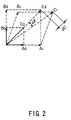
- the vectors A, B and C during small-signal operation are indicated particularly at A 0, B 0 and C 0 , respectively.
- the vectors A, B and C during large-signal operation are indicated particularly at A 1 , B 1 , and C 1 , respectively.
- the vector B 0 changes to the vector B 1 due to a nonlinear increase in amplitude and also due to a change in phase.
- Symbol B 2 indicates a vector plotted on the assumption that the vector B 0 increases only in amplitude in proportion to (namely, linearly with respect to) the input signal while the phase thereof remains unchanged, and C 2 indicates the resultant of the vectors B 2 and A 1 .
- the resultant C 1 of the vectors A 1 and B 1 is greater in amplitude by ⁇ C and has a phase difference of ⁇ .
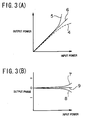
- the compensated circuit 1 has a nonlinear input power-to-output power characteristic as indicated by curve 4 in FIG. 3(A), for example.
- a parallel circuit composed of the aforementioned linear operating means 2 and nonlinear operating means 3 imparts the amplitude increment ⁇ C, and therefore, the parallel circuit shows an input power-to-output power characteristic as indicated by curve 5 in FIG. 3(A). Accordingly, by connecting the compensated circuit 1 and the parallel circuit in series with each other, it is possible to compensate for the nonlinearity of the compensated circuit 1 and thus to obtain a post-compensation characteristic close to ideal line 6 in FIG. 3(A).
- the compensated circuit 1 has a nonlinear input power-to-output phase characteristic as indicated by curve 7 in FIG. 3(B), for example.
- the parallel circuit composed of the linear operating means 2 and the nonlinear operating means 3 provides the phase difference ⁇ ; therefore, the parallel circuit exhibits an input power-to-output phase characteristic as indicated by curve 8 in FIG. 3(B). Accordingly, by connecting the compensated circuit 1 and the parallel circuit in series with each other, it is possible to compensate for the nonlinearity of the compensated circuit 1 and to obtain a post-compensation characteristic close to ideal line 9 in FIG. 3(B).
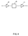
- FIG. 4 is a block diagram showing an RF circuit of a radio transmitter provided with the nonlinear compensating circuit. Specifically, in the RF circuit which includes a power amplifier 11, a small-signal amplifier 12, etc., a compensating circuit 13 is arranged at a stage preceding the power amplifier 11. The power amplifier 11 corresponds to the compensated circuit 1 in FIG. 1.
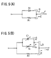
- FIG. 5(A) is a circuit diagram showing the internal arrangement of the compensating circuit 13.
- the compensating circuit 13 comprises a parallel circuit consisting of a diode D1 and a resistor R1.
- the diode D1 corresponds to the nonlinear operating means 3 in FIG. 1
- the resistor R1 corresponds to the linear operating means 2 in FIG. 1.
- a Schottky barrier diode with a small ON-state voltage, in particular, is used, whereby nonlinear operation is available also when a small signal is input.
- symbols D, E and F represent, respectively, the vector of a signal which has passed through the diode D1, the vector of a signal which has passed through the resistor R1, and the vector of a composite signal which is a combination of the two signals and which is input to the power amplifier 11.
- FIG. 5(B) shows an equivalent circuit of the compensating circuit 13 in FIG. 5(A).
- the diode D1 can be represented by a parallel circuit composed of a junction capacitance C1 and an internal resistance r D .
- the junction capacitance C1 takes a slightly greater value than that during small-signal operation
- the internal resistance r D takes a significantly smaller value than that during small-signal operation.
- the vector of a signal which has passed through the junction capacitance C1 is G and that the vector of a signal which has passed through the internal resistance r D is H.
- D 0 , E 0 , F 0 , G 0 and H 0 respectively indicate the vectors D, E, F, G and H during small-signal operation and that D 1 , E 1 , F 1 , G 1 and H 1 respectively indicate the vectors D, E, F, G and H during large-signal operation.
- FIG. 6 is a vector diagram of the compensating circuit 13 shown in FIGS. 5(A) and 5(B).
- FIGS. 5(A) and 5(B) As shown in FIGS. 5(A) and 5(B), as the input signal increases in value, only the amplitude of the vector E 0 increases in proportion to the input signal up to the vector E 1 while the phase of the same vector remains unchanged.
- the vectors G 0 and H 0 their phases remain unchanged but their amplitudes undergo a nonlinear change.
- Symbol D 2 indicates a vector plotted on the assumption that the vector D 0 increases only in amplitude in proportion to (namely, linearly with respect to) the input signal while the phase thereof remains unchanged
- F 2 indicates the resultant vector of the vectors D 2 and E 1 .
- the resultant vector F 1 of the vectors D 1 and E 1 is greater in amplitude by ⁇ F and has a phase difference of ⁇ F .
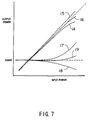
- FIG. 7 shows an example of actual operation of the power amplifier 11 of FIG. 4 which is used as a transmission power amplifier for a portable telephone, wherein the Schottky barrier diode "1SS283" is used as the diode D1 of the compensating circuit 13 shown in FIG. 5 and the resistance of the resistor R1 is 100 ⁇ .
- the power amplifier 11 has an input power-to-output power characteristic indicated by curve 14
- the compensating circuit 13 has an input power-to-output power characteristic indicated by curve 15, and since the compensating circuit 13 and the power amplifier 11 are connected in series with each other, a characteristic curve 16 close to an ideal linear characteristic (dashed line) can be obtained.
- the power amplifier 11 has an input power-to-output phase characteristic indicated by curve 17
- the compensating circuit 13 has an input power-to-output phase characteristic indicated by curve 18, and since the compensating circuit 13 and the power amplifier 11 are connected in series with each other, a characteristic curve 19 close to an ideal linear characteristic (dashed line) can be obtained.
- a Schottky barrier diode is used as the diode D1, but an ordinary diode whose internal resistance has a nonlinear characteristic may be used instead.
- the arrangement according to the second embodiment is basically identical with that of the first embodiment; namely, the second embodiment is identical in arrangement with the first embodiment shown in FIG. 4 but differs therefrom in the internal arrangement of the compensating circuit 13. Therefore, in the following description of the second embodiment, reference should also be made to the arrangement shown in FIG. 4.
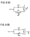
- FIG. 8(A) is a circuit diagram showing the internal arrangement of a compensating circuit according to the second embodiment.
- the compensating circuit comprises a parallel circuit composed of an FET (field-effect transistor) Q1 and a capacitor C2.
- the FET Q1 corresponds to the nonlinear operating means 3 in FIG. 1 and the capacitor C2 corresponds to the linear operating means 2 in FIG. 1.
- the FET Q1 has a source and a drain connected to the input and output sides, respectively, and has a gate grounded.
- the FET Q1 has a property that its source-drain resistance r SD varies in accordance with electric power applied between the source and the gate, thereby achieving nonlinear operation.
- J, I and K respectively indicate the vector of a signal which has passed through the FET Q1, the vector of a signal which has passed through the capacitor C2, and the vector of a composite signal which is a combination of the two signals and which is input to the power amplifier 11.
- FIG. 8(B) shows an equivalent circuit of the compensating circuit shown in FIG. 8(A).
- the FET Q1 can be represented by the source-drain resistance r SD .
- the source-drain resistance r SD takes a significantly smaller value than that during small-signal operation. It is assumed that I 0 , J 0 and K 0 respectively indicate the vectors I, J and K during small-signal operation and that I 1 , J 1 and K 1 respectively indicate the vectors I, J and K during large-signal operation.
- FIG. 9 is a vector diagram of the compensating circuit shown in FIG. 8.
- the input signal increases in value, only the amplitude of the vector I 0 increases in proportion to the input signal up to the vector I 1 , while the phase of the same vector remains unchanged.
- the vector J in the case of the vector J 0, its phase remains unchanged but its amplitude undergoes a nonlinear increase and becomes the vector J 1 .
- Symbol J 2 indicates a vector plotted on the assumption that the vector J 0 increases in amplitude in proportion to (namely, linearly with respect to) the input signal, and K 2 indicates the resultant of the vectors J 2 and I 1 .
- the resultant K 1 of the vectors I 1 and J 1 is greater in amplitude by ⁇ K and has a phase difference of ⁇ K .
- the arrangement according to the third embodiment is basically identical with that of the first embodiment; namely, the third embodiment is identical in arrangement with the first embodiment shown in FIG. 4 but differs therefrom in the internal arrangement of the compensating circuit 13. Therefore, in the following description of the third embodiment, reference should be made also to the arrangement shown in FIG. 4.
- FIG. 10(A) is a circuit diagram showing the internal arrangement of a compensating circuit according to the third embodiment.
- the compensating circuit comprises a parallel circuit composed of an FET (field-effect transistor) Q2 and a coil L1.
- the FET Q2 corresponds to the nonlinear operating means 3 in FIG. 1 and the coil L1 corresponds to the linear operating means 2 in FIG. 1.
- the FET Q2 has a source and a drain connected to the input and output sides, respectively, and has a gate grounded.
- the source-drain resistance r SD of the FET Q2 varies in accordance with electric power applied between the source and the gate.
- N, M and P respectively indicate the vector of a signal which has passed through the FET Q2, the vector of a signal which has passed through the coil L1, and the vector of a composite signal which is a combination of the two signals and which is input to the power amplifier 11.
- FIG. 10(B) shows an equivalent circuit of the compensating circuit shown in FIG. 10(A).
- the FET Q2 can be represented by the source-drain resistance r SD .
- the source-drain resistance r SD takes a significantly smaller value than that during small-signal operation. It is assumed that M 0 , N 0 and P 0 respectively indicate the vectors M, N and P during small-signal operation and that M 1 , N 1 and P 1 respectively indicate the vectors M, N and P during large-signal operation.
- FIG. 11 is a vector diagram of the compensating circuit shown in FIGS. 10(A) and 10(B).
- the input signal increases in value, only the amplitude of the vector M 0 increases in proportion to the input signal up to the vector M 1 while the phase of the same vector remains unchanged.
- the vector N 0 its phase remains unchanged but its amplitude undergoes a nonlinear increase and becomes the vector N 1 .
- Symbol N 2 indicates a vector plotted on the assumption that the vector N 0 increases in amplitude in proportion to (namely, linearly with respect to) the input signal, and P 2 indicates the resultant of the vectors N 2 and M 1 .
- the resultant P 1 of the vectors M 1 and N 1 is greater in amplitude by ⁇ P and has a phase difference of ⁇ P .
- the direction in which the phase difference ⁇ P takes place is opposite to that of the first and second embodiments. Therefore, the third embodiment is especially useful in cases where the direction in which the phase of the power amplifier 11 deviates during large-signal operation is opposite to that of the first and second embodiments.
- a resistor, a capacitor or a coil is singly used as the nonlinear operating means 3, but two or more of these elements may be combined to constitute a parallel or series circuit serving as the nonlinear operating means 3.
- FIGS. 12 (A) and 12 (B) are each a block diagram showing a frequency converting circuit of a radio transmitter provided with a nonlinear compensating circuit.
- a nonlinear compensating circuit 21 is provided for the frequency converting circuit.
- a terminal 23 is supplied with an IF signal
- a terminal 24 is supplied with a local oscillation signal
- a mixer 22 performs frequency conversion and outputs an RF signal from a terminal 25.
- the nonlinear compensating circuit 21 is arranged on the input side of the frequency converting circuit as shown in FIG. 12(A), or is arranged on the output side of the frequency converting circuit as shown in FIG. 12(B).
- the nonlinear compensating circuit 21 has an internal arrangement identical with that of the compensating circuit according to the first, second or third embodiment.
- FIG. 13 is a block diagram showing an RF circuit of a radio transmitter provided with a nonlinear compensating circuit.
- the RF circuit of the radio transmitter includes an automatic level control (ALC) circuit.
- ALC automatic level control
- the output of a power amplifier 34 is detected by a detector 35 to obtain a direct-current voltage corresponding to the output level of the power amplifier 34, and this direct-current voltage is amplified by a direct-current amplifier 36 and fed back to a variable gain amplifier 32.
- the variable gain amplifier 32 adjusts the gain so that the output of the power amplifier 34 may be constant, and the output of the variable gain amplifier 32 is supplied to the power amplifier 34 through a variable attenuator 33.
- a nonlinear compensating circuit 31 is arranged between the variable gain amplifier 32 and the variable attenuator 33.
- the nonlinear compensating circuit 31 has an internal arrangement identical with that of the compensating circuit according to the first, second or third embodiment.
- the power amplifier 34 is the compensated circuit.
- the nonlinear compensating circuit 31 operates in the same manner as described with reference to the first to third embodiments.
- the variable attenuator 33 is used to match the operation level of the power amplifier 34 with that of the nonlinear compensating circuit 31.
- the output level of the power amplifier 34 is controlled to a constant level even in the case where the quantity of attenuation of the variable attenuator 33 is changed, thus facilitating the matching of the operation levels of the nonlinear compensating circuit 31 and power amplifier 34 with each other.
- the variable attenuator 33 may be omitted from the circuit arrangement shown in FIG. 13 to thereby simplify the structure.
- a parallel circuit composed of linear operating means, which performs a linear operation, and nonlinear operating means, which performs a nonlinear operation is connected in series with a compensated circuit, whereby the nonlinear characteristic of the compensated circuit can be compensated for. Accordingly, the nonlinear compensating circuit of the present invention is simplified in structure, compared with the conventional pre-compensating circuit, is reduced in bulk and weight and inexpensive.
- the present invention when used in combination with a power amplifier or the like of a radio apparatus arranged in a base station, the apparatus can be reduced in size and cost. Also, the present invention makes it possible to incorporate a nonlinear compensating circuit into a portable telephone, thus eliminating the problem of increased power consumption by a power amplifier etc.
Landscapes
- Physics & Mathematics (AREA)
- Nonlinear Science (AREA)
- Engineering & Computer Science (AREA)
- Power Engineering (AREA)
- Amplifiers (AREA)
Applications Claiming Priority (3)
| Application Number | Priority Date | Filing Date | Title |
|---|---|---|---|
| JP8003870A JPH09199948A (ja) | 1996-01-12 | 1996-01-12 | 非線形補償回路 |
| JP387096 | 1996-01-12 | ||
| JP3870/96 | 1996-01-12 |
Publications (2)
| Publication Number | Publication Date |
|---|---|
| EP0784379A1 true EP0784379A1 (fr) | 1997-07-16 |
| EP0784379B1 EP0784379B1 (fr) | 2002-09-04 |
Family
ID=11569232
Family Applications (1)
| Application Number | Title | Priority Date | Filing Date |
|---|---|---|---|
| EP96110305A Expired - Lifetime EP0784379B1 (fr) | 1996-01-12 | 1996-06-26 | Circuit de compensation non-linéaire |
Country Status (5)
| Country | Link |
|---|---|
| US (1) | US5884150A (fr) |
| EP (1) | EP0784379B1 (fr) |
| JP (1) | JPH09199948A (fr) |
| CN (1) | CN1073759C (fr) |
| DE (1) | DE69623433T2 (fr) |
Cited By (1)
| Publication number | Priority date | Publication date | Assignee | Title |
|---|---|---|---|---|
| EP0899870A1 (fr) * | 1997-08-27 | 1999-03-03 | Harris Corporation | Dispositif et méthode pour la correction de prédistorsion d'un amplificateur de puissance |
Families Citing this family (3)
| Publication number | Priority date | Publication date | Assignee | Title |
|---|---|---|---|---|
| US6321072B1 (en) * | 1998-08-31 | 2001-11-20 | Conexant Systems, Inc. | Distortion control feedback loop utilizing a non-linear transfer function generator to compensate for non-linearities in a transmitter circuit |
| EP2660984B1 (fr) * | 2011-12-01 | 2016-03-23 | Huawei Technologies Co., Ltd. | Dispositif de compensation de signal optique |
| CN107367319A (zh) * | 2017-02-28 | 2017-11-21 | 淮阴师范学院 | 电容称重传感器非线性补偿的小波神经网络方法 |
Citations (7)
| Publication number | Priority date | Publication date | Assignee | Title |
|---|---|---|---|---|
| GB1419519A (en) * | 1972-10-02 | 1975-12-31 | Pye Ltd | Correcting amplifier non-linearity |
| EP0047825A1 (fr) * | 1980-09-04 | 1982-03-24 | ANT Nachrichtentechnik GmbH | Procédé de linéarisation en bande large d'amplificateurs micro-onde |
| EP0289130A2 (fr) * | 1987-04-28 | 1988-11-02 | Racal Communications Equipment Limited | Emetteurs radio |
| EP0522706A2 (fr) * | 1991-07-06 | 1993-01-13 | Racal Communications Systems Limited | Systèmes d'amplification |
| EP0524008A1 (fr) * | 1991-07-19 | 1993-01-20 | Matsushita Electronics Corporation, Ltd. | Transmetteur à circuits de correction de non-linéarité |
| US5221908A (en) * | 1991-11-29 | 1993-06-22 | General Electric Co. | Wideband integrated distortion equalizer |
| EP0576341A1 (fr) * | 1992-06-26 | 1993-12-29 | Thomson-Lgt Laboratoire General Des Telecommunications | Dispositif d'amplification de puissance d'un signal composite |
Family Cites Families (1)
| Publication number | Priority date | Publication date | Assignee | Title |
|---|---|---|---|---|
| GB2164823A (en) * | 1984-09-17 | 1986-03-26 | Philips Electronic Associated | Television transmitter |
-
1996
- 1996-01-12 JP JP8003870A patent/JPH09199948A/ja not_active Withdrawn
- 1996-06-24 US US08/669,176 patent/US5884150A/en not_active Expired - Lifetime
- 1996-06-26 DE DE69623433T patent/DE69623433T2/de not_active Expired - Fee Related
- 1996-06-26 EP EP96110305A patent/EP0784379B1/fr not_active Expired - Lifetime
- 1996-07-22 CN CN96109935A patent/CN1073759C/zh not_active Expired - Fee Related
Patent Citations (7)
| Publication number | Priority date | Publication date | Assignee | Title |
|---|---|---|---|---|
| GB1419519A (en) * | 1972-10-02 | 1975-12-31 | Pye Ltd | Correcting amplifier non-linearity |
| EP0047825A1 (fr) * | 1980-09-04 | 1982-03-24 | ANT Nachrichtentechnik GmbH | Procédé de linéarisation en bande large d'amplificateurs micro-onde |
| EP0289130A2 (fr) * | 1987-04-28 | 1988-11-02 | Racal Communications Equipment Limited | Emetteurs radio |
| EP0522706A2 (fr) * | 1991-07-06 | 1993-01-13 | Racal Communications Systems Limited | Systèmes d'amplification |
| EP0524008A1 (fr) * | 1991-07-19 | 1993-01-20 | Matsushita Electronics Corporation, Ltd. | Transmetteur à circuits de correction de non-linéarité |
| US5221908A (en) * | 1991-11-29 | 1993-06-22 | General Electric Co. | Wideband integrated distortion equalizer |
| EP0576341A1 (fr) * | 1992-06-26 | 1993-12-29 | Thomson-Lgt Laboratoire General Des Telecommunications | Dispositif d'amplification de puissance d'un signal composite |
Cited By (2)
| Publication number | Priority date | Publication date | Assignee | Title |
|---|---|---|---|---|
| EP0899870A1 (fr) * | 1997-08-27 | 1999-03-03 | Harris Corporation | Dispositif et méthode pour la correction de prédistorsion d'un amplificateur de puissance |
| US6054895A (en) * | 1997-08-27 | 2000-04-25 | Harris Corporation | Apparatus and method for pre-distortion correction of a power amplifier stage |
Also Published As
| Publication number | Publication date |
|---|---|
| US5884150A (en) | 1999-03-16 |
| DE69623433T2 (de) | 2003-06-05 |
| JPH09199948A (ja) | 1997-07-31 |
| CN1073759C (zh) | 2001-10-24 |
| DE69623433D1 (de) | 2002-10-10 |
| EP0784379B1 (fr) | 2002-09-04 |
| CN1155184A (zh) | 1997-07-23 |
Similar Documents
| Publication | Publication Date | Title |
|---|---|---|
| JP3708232B2 (ja) | 歪補償回路を有する送信装置 | |
| US7260157B2 (en) | Phase shifted transmitter architecture for communication systems | |
| US5142240A (en) | Amplifier circuit with correction of amplitude and phase distortions | |
| US8180304B2 (en) | Efficient power amplifier | |
| US5101172A (en) | Linear amplifier | |
| US7893763B2 (en) | Apparatus and method for power added efficiency optimization of high amplification applications | |
| EP2418767B1 (fr) | Dispositif d'amplification | |
| JPH08274559A (ja) | 出力電力制御装置 | |
| US20070147541A1 (en) | Transmitter apparatus and wireless communication apparatus | |
| US10992268B2 (en) | Radio frequency amplification device capable of detecting the frequency band | |
| US12438507B2 (en) | Power amplifier circuit, radio-frequency circuit, and communication device | |
| US7139535B2 (en) | Signal processing of an amplitude-modulated and/or phase-modulated high-frequency signal | |
| US5444399A (en) | Mixer circuit | |
| US5334945A (en) | Power control circuit | |
| KR100346324B1 (ko) | 왜곡 보상 회로 | |
| US5884150A (en) | Nonlinear compensating circuit | |
| JP3429395B2 (ja) | アナログ光信号伝送用適応等化器 | |
| US20040085127A1 (en) | Power amplifying method, power amplifier, and communication apparatus | |
| US8369446B2 (en) | Transmitter | |
| US6710716B1 (en) | Power detecting circuit and demodulator comprising the same | |
| JP2003179444A (ja) | 電圧制御電力増幅器 | |
| US20080299920A1 (en) | Transmission Device | |
| CA2298317C (fr) | Amplificateur de puissance | |
| JPH05167352A (ja) | 周波数変換装置 | |
| GB2259628A (en) | Transmitter power control unit |
Legal Events
| Date | Code | Title | Description |
|---|---|---|---|
| PUAI | Public reference made under article 153(3) epc to a published international application that has entered the european phase |
Free format text: ORIGINAL CODE: 0009012 |
|
| AK | Designated contracting states |
Kind code of ref document: A1 Designated state(s): DE FR GB |
|
| 17P | Request for examination filed |
Effective date: 19970730 |
|
| 17Q | First examination report despatched |
Effective date: 19991210 |
|
| GRAG | Despatch of communication of intention to grant |
Free format text: ORIGINAL CODE: EPIDOS AGRA |
|
| GRAG | Despatch of communication of intention to grant |
Free format text: ORIGINAL CODE: EPIDOS AGRA |
|
| GRAH | Despatch of communication of intention to grant a patent |
Free format text: ORIGINAL CODE: EPIDOS IGRA |
|
| GRAH | Despatch of communication of intention to grant a patent |
Free format text: ORIGINAL CODE: EPIDOS IGRA |
|
| GRAA | (expected) grant |
Free format text: ORIGINAL CODE: 0009210 |
|
| AK | Designated contracting states |
Kind code of ref document: B1 Designated state(s): DE FR GB |
|
| REG | Reference to a national code |
Ref country code: GB Ref legal event code: FG4D |
|
| REF | Corresponds to: |
Ref document number: 69623433 Country of ref document: DE Date of ref document: 20021010 |
|
| ET | Fr: translation filed | ||
| PLBE | No opposition filed within time limit |
Free format text: ORIGINAL CODE: 0009261 |
|
| STAA | Information on the status of an ep patent application or granted ep patent |
Free format text: STATUS: NO OPPOSITION FILED WITHIN TIME LIMIT |
|
| 26N | No opposition filed |
Effective date: 20030605 |
|
| PGFP | Annual fee paid to national office [announced via postgrant information from national office to epo] |
Ref country code: FR Payment date: 20040608 Year of fee payment: 9 |
|
| PGFP | Annual fee paid to national office [announced via postgrant information from national office to epo] |
Ref country code: GB Payment date: 20040623 Year of fee payment: 9 |
|
| PGFP | Annual fee paid to national office [announced via postgrant information from national office to epo] |
Ref country code: DE Payment date: 20040708 Year of fee payment: 9 |
|
| PG25 | Lapsed in a contracting state [announced via postgrant information from national office to epo] |
Ref country code: GB Free format text: LAPSE BECAUSE OF NON-PAYMENT OF DUE FEES Effective date: 20050626 |
|
| PG25 | Lapsed in a contracting state [announced via postgrant information from national office to epo] |
Ref country code: DE Free format text: LAPSE BECAUSE OF NON-PAYMENT OF DUE FEES Effective date: 20060103 |
|
| PG25 | Lapsed in a contracting state [announced via postgrant information from national office to epo] |
Ref country code: FR Free format text: LAPSE BECAUSE OF NON-PAYMENT OF DUE FEES Effective date: 20060228 |
|
| GBPC | Gb: european patent ceased through non-payment of renewal fee |
Effective date: 20050626 |
|
| REG | Reference to a national code |
Ref country code: FR Ref legal event code: ST Effective date: 20060228 |