EP0785473A2 - Reduzierung der Schäden in optischen Elementen bei lithographischen Herstellungsverfahren - Google Patents
Reduzierung der Schäden in optischen Elementen bei lithographischen Herstellungsverfahren Download PDFInfo
- Publication number
- EP0785473A2 EP0785473A2 EP97300183A EP97300183A EP0785473A2 EP 0785473 A2 EP0785473 A2 EP 0785473A2 EP 97300183 A EP97300183 A EP 97300183A EP 97300183 A EP97300183 A EP 97300183A EP 0785473 A2 EP0785473 A2 EP 0785473A2
- Authority
- EP
- European Patent Office
- Prior art keywords
- pulses
- pulse
- primary
- subsystem
- exposure source
- Prior art date
- Legal status (The legal status is an assumption and is not a legal conclusion. Google has not performed a legal analysis and makes no representation as to the accuracy of the status listed.)
- Granted
Links
Images


Classifications
-
- G—PHYSICS
- G03—PHOTOGRAPHY; CINEMATOGRAPHY; ANALOGOUS TECHNIQUES USING WAVES OTHER THAN OPTICAL WAVES; ELECTROGRAPHY; HOLOGRAPHY
- G03F—PHOTOMECHANICAL PRODUCTION OF TEXTURED OR PATTERNED SURFACES, e.g. FOR PRINTING, FOR PROCESSING OF SEMICONDUCTOR DEVICES; MATERIALS THEREFOR; ORIGINALS THEREFOR; APPARATUS SPECIALLY ADAPTED THEREFOR
- G03F7/00—Photomechanical, e.g. photolithographic, production of textured or patterned surfaces, e.g. printing surfaces; Materials therefor, e.g. comprising photoresists; Apparatus specially adapted therefor
- G03F7/70—Microphotolithographic exposure; Apparatus therefor
- G03F7/70483—Information management; Active and passive control; Testing; Wafer monitoring, e.g. pattern monitoring
- G03F7/7055—Exposure light control in all parts of the microlithographic apparatus, e.g. pulse length control or light interruption
- G03F7/70583—Speckle reduction, e.g. coherence control or amplitude/wavefront splitting
-
- G—PHYSICS
- G03—PHOTOGRAPHY; CINEMATOGRAPHY; ANALOGOUS TECHNIQUES USING WAVES OTHER THAN OPTICAL WAVES; ELECTROGRAPHY; HOLOGRAPHY
- G03F—PHOTOMECHANICAL PRODUCTION OF TEXTURED OR PATTERNED SURFACES, e.g. FOR PRINTING, FOR PROCESSING OF SEMICONDUCTOR DEVICES; MATERIALS THEREFOR; ORIGINALS THEREFOR; APPARATUS SPECIALLY ADAPTED THEREFOR
- G03F7/00—Photomechanical, e.g. photolithographic, production of textured or patterned surfaces, e.g. printing surfaces; Materials therefor, e.g. comprising photoresists; Apparatus specially adapted therefor
- G03F7/70—Microphotolithographic exposure; Apparatus therefor
- G03F7/70216—Mask projection systems
- G03F7/70241—Optical aspects of refractive lens systems, i.e. comprising only refractive elements
Definitions
- the invention relates to the fabrication of devices using optical lithography and, in particular, to reducing damage to optical elements caused by prolonged exposure to deep ultra-violet (DUV) radiation.
- DUV deep ultra-violet
- optical lithography such as projection printing using steppers and scanners
- Such technique employs an exposure source to image the pattern through an optical system.
- the pattern corresponds to circuit features that comprise various parts of an electronic device.
- the continuing demand for further miniaturization of devices has facilitated the use of exposure sources with shorter wavelengths in order to achieve smaller image resolution.
- projection printers operating in the DUV region (248 nm or shorter) have been able to image linewidths of about 0.25 ⁇ m.
- DUV radiation at least at the intensity levels which are desirable for commercial applications, tends to cause damage to the optical elements in the projection printers.
- the optical system comprises mostly or all transmissive elements.
- One of the few materials for high precision optics which transmits DUV radiation is fused silica. Rothschild et al., Excimer Laser Projection Lithography: Optical Considerations , Microelectronic Engineering Vol. 9, pages 27-29 (1989), which is herein incorporated by reference for all purposes. As such, it has become the material of choice for use in the manufacturing of optical elements for DUV printers.
- the optical system is diffraction limited.
- the specifications of the lenses are well below diffraction limited and balanced in the overall system for small net wavefront aberration. For example, the root mean square (RMS) wavefront error for a typical optical system is about 1/10 th of the wavelength of the exposure source. Even stricter requirements imposed on the individual optical elements make them very sensitive to phenomenon which would alter their behavior.
- RMS root mean square
- the predominant exposure sources used in DUV projection printers are excimer lasers, such as the KrF (248 nm) and ArF (193 m). This is due to the fact that excimer lasers can generate adequate power output (about 2-20 W) necessary to satisfy manufacturing throughput demands.
- the power output of excimer lasers is relatively stable, which is important for dose control. For example, fluctuations in output amplitude of a typical excimer laser is about ⁇ 3%.
- Short pulses are pulses of a frequency F each having a pulse width ( ⁇ ) that is significantly less than the time gap between each pulse (1/F).
- ⁇ the pulse width
- the pulse width begins where the energy of the pulse can be detected by, for example, attenuators or silicon photo-diodes and ends at about the point where 99% of the pulse energy has been detected.
- the pulse width is about 10-30 nsec and F is about 200-500 Hz.
- Each output pulse or shot from an excimer laser is typically about 10-50 mJ.
- fused silica when exposed to such intensity levels at 248 or shorter, is subjected to phenomenon known as laser-induced damage. See Rothschild et al., Excimer Laser Projection Lithography: Optical Considerations , Microelectronic Engineering, Vol. 9, pages 27-29 (1989), which is already incorporated by reference for all purposes.
- the major modes of laser-induced damage in fused silica are color center formation and optical compaction. The formation of E' color centers leads to increased optical absorption at the exposure source wavelength.
- Optical compaction alters the lens dimensionally and increases the index of refraction in the compacted area, thus causing wavefront aberrations such as 1) instantaneous changes in the wavefront properties of the lens as a pulse is transmitted, 2) accumulated changes in the wavefront or overall transmission efficiency of the lens, and 3) thermal degradation of the lens wavefront due to absorption of a larger fraction of power.
- wavefront aberrations such as 1) instantaneous changes in the wavefront properties of the lens as a pulse is transmitted, 2) accumulated changes in the wavefront or overall transmission efficiency of the lens, and 3) thermal degradation of the lens wavefront due to absorption of a larger fraction of power.
- laser-induced damage adversely affects the characteristics of the optical system, thus degrading the performance of projection printers.
- the initial mechanisms causing the damage have been identified as the multi-photon interactions in the material activated by extremely high momentary intensity levels.
- the rate of multi-photon absorption laser-induced damage often has a quadratic dependence to pulse intensity in the practical regime of intensifies that might be used.
- laser-induced damage to the optics is even more severe as the wavelength of the exposure source becomes shorter because fused silica is much more absorptive at shorter wavelengths.
- the rate of laser-induced damage at 193 nm for ArF laser is much greater than that at 248 nm for KrF laser. See Rothschild et al., Excimer Laser Projection Lithography: Optical Considerations , Microelectronic Engineering Vol. 9, pages 27-29 (1989).
- projection lenses with reduction powers may have some elements near the wafer. These elements are exposed to the greatest intensity of energy from each pulse and therefore are most prone to laser induced damage. Moreover, the projection lens is one of the more critical and more expensive elements of the system. From the above description, it is therefore desirable to reduce the rate of damage to the optical system of projection printers and, in particular, to the projection lens of the optical system caused by exposure to DUV energy pulses, particularly as shorter wavelengths, photo resists requiring larger doses, or longer useful lens life becomes desirable.
- the invention is directed to DUV lithography systems and processes for fabricating devices which reduce the rate of laser-induced damage to optical elements caused by exposure to DUV radiation.
- the reduction in the rate of laser-induced damage is achieved by reducing the peak intensity of each pulse without affecting average power output of the exposure source.
- Each primary output pulse from a pulsed DUV source is separated into a plurality of secondary pulses, including at least N secondary pulses where N is greater than or equal to 2.
- the intensity of the secondary pulses is about 1/N th the intensity of the primary output pulse.
- the N secondary pulses are delayed in time so that the majority of the pulse energy of each secondary pulse is from each other, resulting in a sequence of N pulses with lower peak intensity for each primary output pulse.
- These secondary pulses are then appropriately directed through the optical train of the lithography system for imaging a mask pattern on a semiconductor wafer.
- the rate of laser-induced to the optical elements is reduced by about N times.
- these secondary pulses are formed quite efficiently using simple and insensitive illumination optics taht don't complicate or corrupt desirable characteristics of the laser or optics.
- the reduction in damage rate is achieved without substantially decreasing throughput, dose control, or imaging characteristics of the lithography system.
- the present invention relates to reducing laser-induced damage to optical elements caused by exposure to DUV energy pulses from an excimer laser. While illustrative embodiments of the invention are described with specific geometric configuration, it will be apparent to those skilled in the art that a variety of configurations which satisfy geometric requirements for proper lithographic illumination are also useful.
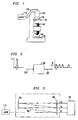
- FIG. 1 is a simplified illustration of a conventional excimer projection printer such as a scanner or stepper for fabricating device.
- a conventional excimer projection printer such as a scanner or stepper for fabricating device.
- the projection printer comprises an excimer exposure source 110, a beam delivery subsystem 120, an illuminator 130, a mask 135 mounted on a mask frame 136, a projection lens 140, and a stage 150.
- excimer laser 110 sends pulses through the beam delivery subsystem.
- the beam delivery subsystem comprises various mirrors and/or reflective elements such as lenses to direct the pulses into the illuminator.
- the beam delivery system includes attenuators, shutters, and devices for providing energy or wavelength measurements, as known in the art.
- the illuminator receives the pulses and spatially manipulates the energy from the pulses to provide optimum illumination of mask 135, which contains, for example, circuit patterns.
- Projection lens 140 projects the image of the mask onto a wafer 145 mounted on stage 150.
- the stage includes precision translation and rotation control by a computer (not shown) for accurate pattern alignment.
- fused silica the material from which the optical elements of the DUV projection printers are often made, is subjected to laser-induced damage when exposed to DUV radiation.
- the rate of laser-induced damage (D) in fused silica has been found to have a linear dependence with the number of pulses and a quadratic dependence with the peak power-density within a laser pulse. See Hibbs et al., 193-nm Lithography at MIT Lincoln Lab , Solid State Technology, July 1995, and Yamagata, Degradation of Transmission of Silica glass on Excimer Laser Irradiation , Journal of the Ceramic Society of Japan, volume 100 (1992).
- D a*E 2 *J
- E the energy density per pulse (mJ/cm 2 ) impinging on the optical element
- J the number of pulses
- a scaling constant
- the actual decrease in damage rate varies due to losses that can occur in the transmission of the radiation.
- a divide and delay (DD) subsystem is employed to reduce the damage rate to the optical components of the projection printer by reducing the peak intensity (E) of the excimer pulses. Furthermore, this reduction, as will be apparent, is achieved at essentially the same average power output level as projection printers without the DD optical subsystem. Therefore, the DD subsystem induces the damage rate without adversely affecting the throughput of the projection printers.
- DD optical subsystem 200 receives primary input pulses 210 from the excimer laser for processing.
- the DD subsystem then outputs the processed input pulses 220 to the illuminator.
- the DD subsystem is described as a discrete unit which is spatially located between the laser and illuminator, it will be to those skilled in the art that the DD subsystem can be, for example, incorporated as part of the illuminator, beam delivery subsystem or enclosed in the cabinet of the source laser.
- Processing of the primary input pulses 210 involves reducing the peak intensity of each primary pulse.
- the rate of laser-induced damage to the optical elements downstream from the DD subsystem is decreased.
- Reduction in peak intensity is achieved by dividing each primary input pulse into N secondary pulses and incrementally delaying each N secondary pulse. As such, the secondary pulses, as they are output from the DD subsystems, are staggered.
- the N secondary pulses are confined within the time gap between the arrival of the next primary pulse.
- some energy may be lost due to transmission in the DD subsystem, but this loss may be negligible as highly efficient optical components or nearly lossless elements such as reflectors can be employed.
- the time gap between each primary pulse is very large compared to the pulse width, e.g., by a factor of 10 5
- the number of secondary pulses into which the primary pulse can be divided before the arrival of the next primary pulse is significant. In fact, this number is much greater than the number which is practical for implementing the DD subsystem. For example, the larger the number of secondary pulses, the more complex the DD subsystem becomes.
- the number of secondary pulses formed is between 2 to 20.
- the number of secondary pulses formed is between 2 to 15, more preferably, between 2 to 10, even more preferably, between 2 to 7, and most preferably, between 2 to 5.
- the upper limit on the number of secondary pulses is dependent on 1) the pulse width of the secondary pulses, 2) length of delay between each secondary pulse, and 3) the length of the time gap between successive primary pulses.
- the amount that the peak intensity of each primary pulse is reduced depends on the number of times that the primary pulse is divided (i.e., the number of resulting secondary pulses) and the length of delay between each secondary pulse. For example, assuming that there is negligible or no loss in pulse energy from the elements in the DD subsystem and that each resulting secondary pulse has about the same peak intensity, dividing the primary pulse by N secondary pulses and delaying each successive secondary pulse by at least a pulse width would result in a reduction in peak intensity by about N times (1/N). Delays between successive secondary pulses of less than a pulse width reduces the peak intensity by less than N times. As such, the reduction in the rate of damage decreases as the delay between the successive secondary pulses and/or as the number of secondary pulses become smaller.
- the delay between each secondary pulse is at least equal to about a pulse width.
- the delay between each secondary pulse is less than pulse width, but long enough to provide a reduction in peak intensity such that the rate of laser-induced damage is reduced. It will be appreciated that the delays between each successive pulse need not be equal in order to achieve a reduction in the peak intensity of the primary pulses.
- each successive secondary output pulse should travel an additional distance of at least about one foot for each nanosecond of delay.
- the difference between each successive secondary pulse path is at least about 20 feet.
- FIG. 3 is an illustrative embodiment of the DD subsystem 200 for splitting a primary input pulse P into secondary pulses P1, P2, and P3.
- the DD subsystem comprises an efficient reflector 320 and segmented partial (SP) reflector 340.
- Reflector 320 can be any conventional reflector used for reflecting DUV radiation.
- pulse P enters the DD subsystem it follows a path to the SP reflector which divides pulse P into P1 and P1a.
- the SP reflector passes P1 while reflecting P1a toward reflector 320.
- Reflector 320 then reflects P1a back toward SP reflector to divide P1a into P2 and P3.
- P2 passes through to the illuminator as P3 is reflected toward reflector 320.
- P3 is then reflected back at the SP reflector which transmits P3 to the illuminator.
- Reflector 220 and SP reflector 340 are each spatially separated by a distance d.
- the geometry of the DD subsystem provides a delay for each successive beam path which is equal to about the time it takes for light to travel a distance of 2*d.
- d is at least 10 feet to provide a delay of at least 20 nsec, which is the pulse width for a typical excimer pulse.
- folding mirrors can advantageously be located within the beam paths to compress the size of the DD subsystem.
- FIG. 4 illustrates SP reflector 340 of the DD subsystem used for splitting a primary pulse into secondary pulses.
- the SP reflector is made from, for example, fused silica 510 or other known suitable material. Such reflectors, for example are available from Rocky Mountain Instruments of Longmont, CO.
- the SP reflector is divided into three distinct zones, Z 1 , Z 2 , and Z 3 .
- the zones are coated with conventional DUV reflective material using well-known coating techniques.
- the reflectivity of each zone is calculated to appropriately divide the beam into secondary output pulses with the desired intensity.
- Various techniques which are known in the art can be used to achieve the desired reflectivity in each zone.
- the reflectivity of each zone is chosen to produce secondary pulses of about the same total energy level.
- each zone should be large enough to capture the shape of the excimer pulse, which typically is about 5x20 mm.
- the size of each zone is about 10-20% larger than the beam profile, leaving about a 1-2 mm boundary surrounding the beam. This is often useful in facilitating the coating process.
- FIG. 5 illustrates an embodiment of one type of conventional DUV illuminator 600.
- illuminators are described in Ichihara et al., Illumination System of an Excimer Laser Stepper , SPIE Vol. 1138, 137 (1989), which is herein incorporated by reference for all purposes.
- the illuminator comprises expanding optics 610, lens array 620, and a condenser lens 630.
- a pulse from an excimer laser passes through the expanding optics comprising, for example, cylindrical lenses 611 and 612.
- the cylindrical lenses transform the rectangular beam shape into a square beam to fill the lens array, such as a fly's-eye lens.
- the fly's-eye lens comprises 100 lenses or lenslets, e.g., 10X10 array.
- the fly's-eye lens samples or breaks up the beam into aerial portions associated with each lenslet. Each sample is diverged by the associated lenslet and then directed at the reticle by the condenser lens.
- the condenser lens is spatially located so that the lens allay is in its front focal plane and a mask 650 is in its back focal plane.
- Each lenslet in connection with the condenser acts as a telescope to expand the sample.
- the expanded profile samples are added at the reticle in such a way that the original beam profile averages out to a substantially uniform result.
- the function of the illuminator is to provide substantially uniform illumination of the mask, both on a large scale and microscopic level.
- Non-uniform illumination can create undesirable interference patterns (i.e., "speckle") or large scale inconsistency in the image that is formed on the wafer.
- spekle undesirable interference patterns
- Valiev, et al. The Optimization of Excimer Lasers Radiation Characteristics for Projection Lithography, JJAP Series 3, Proc. of 1989 Intern. Symp. on MicroProcess Conference, pp. 37, which is herein incorporated by reference for all purposes for a discussion on uniformity and coherence of the excitation source.
- Acceptable uniformity of the illumination depends on the fact that the emerging light from each lenslet is relatively incoherent.
- a problem with some conventional illuminators is that the expander optics used to fill the fly's-eye lens array may adversely affect uniform illumination of the mask. This is because the spatial coherence of the input pulse is increased as it is being magnified by the expanding optics. Greater coherence in the pulse causes the whole matrix of samples from the lens array to have too many correlated or partly coherent secondary beams. As a result, interference patterns or larger-scale effects of coherent summing are present in the image that formed on the wafer.
- the use of DD subsystem advantageously fills the fly's eye lens array without requiring expanding optics.
- the geometry which generates large delays also assures that the portions of the lens array are incoherently illuminated since coherence length is typically a few centimeters.
- a modified illuminator 700 comprising a condenser lens 710 and a lens array 720 located at the front focal plane of the condenser lens is shown.
- the DD subsystem divides the primary input pulse into secondary pulses P1-P5 for input into the illuminator.
- the secondary outputs have different parallel beam paths with each being separated in time. Consequently, each pulse contacts a different part of the lens array at different instants in time. It should be appreciated by those skilled in the art that the separation of the secondary beam paths should be such that the different parts of the fly's eye lens array are contacted by the secondary pulses.
- the secondary pulses effectively scan the lens array to smear away the unwanted coherent patterning.
- the DD subsystem ensures that the secondary output pulses are incoherent because the separation between each successive secondary output pulse is significantly greater than about 20 mm, which is typically the extent of the longitudinal coherence of an excimer pulse. For example, a typical excimer pulse with a pulse width of 20 nsec would require a separation of about 20 feet in order to achieve secondary pulse separation of about a pulse width. As such, the DD subsystem provides an additional benefit of decreasing the visibility of interference patterns because the lens array is filled with pulses which have lower coherence than those in conventional illuminators.
- the beam paths are illustratively shown as a planar arrangement in 2-dimensional space, it will be understood that there are virtually unlimited degrees of freedom available to configure the beam paths in various arrangements, either in 2 or 3 dimensional space and/or arriving at the illuminator in different orders, to take advantage of various specific illuminator designs, as will be apparent to those skilled in the art.
- the secondary pulse profiles can be spatially grouped more closely together at the lens array by using separate reflector segments to create a small overall convergence in the secondary output pulses from the DD subsystem.
- FIG. 7 shows a DD interface used to smooth the secondary output beam paths from the DD subsystem for input into a conventional excimer illuminator 130.
- the DD interface comprises faceted mirrors 810-830 and reflector 850.
- the faceted mirrors and the reflector in combination, converge the output pulses P1, P2 and P3 at a small angle.
- the pulses overlap and enter the illuminator in substantially a single path, one at a time.
- the secondary pulses are in a 1-dimensional configuration, it will be understood that different configurations can be used to take advantage of various illuminator designs. This geometry is advantageous if the lens pupil conjugate to the fly's eye array is prone to damage.
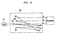
- FIG. 8 illustrates an embodiment of DD subsystem 800 for splitting a primary pulse into secondary pulses using a diffractive element.
- DD subsystem 900 comprises a diffractor 910 and reflectors 920-925.
- Diffractor 910 such as a phase plate or binary optic made by Teledyne Brown Engineering, separates the primary pulse P into secondary output pulses P1, P2, and P3 with separate beam paths.
- reflectors 920-925 are used for folding the multiple beam paths to provide the necessary separation between each output pulse. It will be apparent to those skilled in the art that any geometry for energy separation using various folding schemes are useful to effectively divide and delay the primary pulses into multiple secondary pulses.
- the divide and delay subsystem may be provided by optical elements with other functions, so long as delays of appropriate length are created with the intent to reduce the damage rate. More sophisticated illuminators may, to an even greater extent, benefit from the DD subsystem. For example, an idea illuminator with both reticle field and pupil behavior strongly decoupled from the source will be most easily adapted to take advantage of the damage reduction resulting from the DD subsystem.
- the optical elements which make up the DD subsystem will also be prone to damage. It is possible that the invention will be practical with these elements used as consumables and easily replaced, as is typically done with excimer laser optics.
- the illuminator will be far less sensitive to damage to the projection lens in most cases. Also, the lens or its elements may be expensive or difficult to replace.
- the DD elements may act in a sacrificial manner to protect critical elements.
Landscapes
- Physics & Mathematics (AREA)
- General Physics & Mathematics (AREA)
- Exposure And Positioning Against Photoresist Photosensitive Materials (AREA)
- Exposure Of Semiconductors, Excluding Electron Or Ion Beam Exposure (AREA)
Applications Claiming Priority (2)
| Application Number | Priority Date | Filing Date | Title |
|---|---|---|---|
| US586412 | 1996-01-16 | ||
| US08/586,412 US5891605A (en) | 1996-01-16 | 1996-01-16 | Reduction in damage to optical elements used in optical lithography for device fabrication |
Publications (3)
| Publication Number | Publication Date |
|---|---|
| EP0785473A2 true EP0785473A2 (de) | 1997-07-23 |
| EP0785473A3 EP0785473A3 (de) | 1997-11-26 |
| EP0785473B1 EP0785473B1 (de) | 2000-05-31 |
Family
ID=24345610
Family Applications (1)
| Application Number | Title | Priority Date | Filing Date |
|---|---|---|---|
| EP97300183A Expired - Lifetime EP0785473B1 (de) | 1996-01-16 | 1997-01-14 | Reduzierung der Schäden in optischen Elementen bei lithographischen Herstellungsverfahren |
Country Status (4)
| Country | Link |
|---|---|
| US (1) | US5891605A (de) |
| EP (1) | EP0785473B1 (de) |
| JP (1) | JPH09213628A (de) |
| DE (1) | DE69702147T2 (de) |
Cited By (5)
| Publication number | Priority date | Publication date | Assignee | Title |
|---|---|---|---|---|
| EP0984531A3 (de) * | 1998-09-04 | 2002-09-25 | Cymer, Inc. | Excimerlaser mit Puls- und Strahlvervielfacher |
| WO2003049175A1 (fr) * | 2001-12-07 | 2003-06-12 | Sony Corporation | Irradiateur a faisceaux et dispositif de recuit pour laser |
| EP0943390A3 (de) * | 1998-02-23 | 2004-05-06 | Oramir Semiconductor Equipment Ltd. | Oberflächenbehandlung durch multilaser-Verbrennung |
| US6996141B1 (en) | 1999-07-08 | 2006-02-07 | Carl Zeiss Smt Ag | Device for reducing the peak power of a pulsed laser light source |
| DE102009047098A1 (de) | 2009-11-25 | 2011-05-26 | Carl Zeiss Smt Gmbh | Optische Anordnung zur Homogenisierung eines Laserpulses |
Families Citing this family (6)
| Publication number | Priority date | Publication date | Assignee | Title |
|---|---|---|---|---|
| US6067311A (en) * | 1998-09-04 | 2000-05-23 | Cymer, Inc. | Excimer laser with pulse multiplier |
| US6339505B1 (en) * | 2000-06-26 | 2002-01-15 | International Business Machines Corporation | Method for radiation projection and lens assembly for semiconductor exposure tools |
| US20020074520A1 (en) * | 2000-12-15 | 2002-06-20 | Xerox Corporation | Substantially seamless electrostatographic member fabrication apparatus |
| US7432517B2 (en) * | 2004-11-19 | 2008-10-07 | Asml Netherlands B.V. | Pulse modifier, lithographic apparatus, and device manufacturing method |
| US9793673B2 (en) * | 2011-06-13 | 2017-10-17 | Kla-Tencor Corporation | Semiconductor inspection and metrology system using laser pulse multiplier |
| KR101656588B1 (ko) * | 2011-08-26 | 2016-09-09 | 칼 짜이스 에스엠에스 엘티디 | 포토리소그래피용 광학 소자를 국부적으로 변형하기 위한 방법 및 장치 |
Family Cites Families (6)
| Publication number | Priority date | Publication date | Assignee | Title |
|---|---|---|---|---|
| US3447856A (en) * | 1966-10-07 | 1969-06-03 | Bell Telephone Labor Inc | Optical pulse multiplier |
| JPH01287924A (ja) * | 1988-03-30 | 1989-11-20 | Hitachi Ltd | コヒーレント制御露光装置 |
| US5089711A (en) * | 1990-01-19 | 1992-02-18 | California Jamar, Incorporated | Laser plasma X-ray source |
| US5003543A (en) * | 1990-01-19 | 1991-03-26 | California Jamar, Incorporated | Laser plasma X-ray source |
| EP0648348B1 (de) * | 1993-03-01 | 1999-04-28 | General Signal Corporation | Vorrichtung zur erzeugung einer einstellbaren ringförmigen beleuchtung für einen photolithograpischen projektionsapparat |
| JP2862477B2 (ja) * | 1993-06-29 | 1999-03-03 | キヤノン株式会社 | 露光装置及び該露光装置を用いてデバイスを製造する方法 |
-
1996
- 1996-01-16 US US08/586,412 patent/US5891605A/en not_active Expired - Lifetime
-
1997
- 1997-01-13 JP JP9003816A patent/JPH09213628A/ja active Pending
- 1997-01-14 DE DE69702147T patent/DE69702147T2/de not_active Expired - Fee Related
- 1997-01-14 EP EP97300183A patent/EP0785473B1/de not_active Expired - Lifetime
Cited By (7)
| Publication number | Priority date | Publication date | Assignee | Title |
|---|---|---|---|---|
| EP0943390A3 (de) * | 1998-02-23 | 2004-05-06 | Oramir Semiconductor Equipment Ltd. | Oberflächenbehandlung durch multilaser-Verbrennung |
| EP0984531A3 (de) * | 1998-09-04 | 2002-09-25 | Cymer, Inc. | Excimerlaser mit Puls- und Strahlvervielfacher |
| US6996141B1 (en) | 1999-07-08 | 2006-02-07 | Carl Zeiss Smt Ag | Device for reducing the peak power of a pulsed laser light source |
| WO2003049175A1 (fr) * | 2001-12-07 | 2003-06-12 | Sony Corporation | Irradiateur a faisceaux et dispositif de recuit pour laser |
| US7109435B2 (en) | 2001-12-07 | 2006-09-19 | Sony Corporation | Beam irradiator and laser anneal device |
| DE102009047098A1 (de) | 2009-11-25 | 2011-05-26 | Carl Zeiss Smt Gmbh | Optische Anordnung zur Homogenisierung eines Laserpulses |
| WO2011064059A1 (en) | 2009-11-25 | 2011-06-03 | Carl Zeiss Smt Gmbh | Optical arrangement for homogenizing a laser pulse |
Also Published As
| Publication number | Publication date |
|---|---|
| DE69702147T2 (de) | 2000-11-16 |
| EP0785473B1 (de) | 2000-05-31 |
| EP0785473A3 (de) | 1997-11-26 |
| DE69702147D1 (de) | 2000-07-06 |
| US5891605A (en) | 1999-04-06 |
| JPH09213628A (ja) | 1997-08-15 |
Similar Documents
| Publication | Publication Date | Title |
|---|---|---|
| EP0744664B1 (de) | Hybrides Belichtungssystem für die Photolithographie | |
| JP4169374B2 (ja) | 投影マイクロリソグラフィ装置の照明手段 | |
| JP4437006B2 (ja) | リソグラフィ処理のためのレーザスペクトルエンジニアリング | |
| US7088758B2 (en) | Relax gas discharge laser lithography light source | |
| US7605386B2 (en) | Optical device with raster elements, and illumination system with the optical device | |
| KR19980080521A (ko) | 조명장치 및 이 조명장치를 가진 노광장치 | |
| Dickey | Laser beam shaping | |
| EP0785473B1 (de) | Reduzierung der Schäden in optischen Elementen bei lithographischen Herstellungsverfahren | |
| JP2010529668A (ja) | マイクロリソグラフィツール用の反射照明システム | |
| Himel et al. | Design and fabrication of customized illumination patterns for low-k1 lithography: a diffractive approach | |
| US7326948B2 (en) | Beam modifying device, lithographic projection apparatus, method of treating a beam, and device manufacturing method | |
| US7006198B2 (en) | System and method for laser beam expansion | |
| JP2002198309A (ja) | 熱的な負荷の少ない照明系 | |
| US20060039651A1 (en) | Patterning apparatuses and methods for the same | |
| Kueck et al. | New system for fast submicron laser direct writing | |
| JP5091817B2 (ja) | 電磁放射パルス幅制御装置及び電磁放射パルス幅制御方法 | |
| US5912725A (en) | Illumination optical system to be used in an exposure apparatus and a method of manufacturing a semiconductor structure using the exposure apparatus | |
| US20060268251A1 (en) | Illumination system for a microlithographic projection exposure apparatus | |
| TWI785041B (zh) | 反射系統、微影曝光工具、在工件上形成條紋圖案的方法及微器件的製造方法 | |
| JPS6332555A (ja) | 露光装置 | |
| JP2002057098A (ja) | 照明光学装置,該照明光学装置を備えた露光装置,及びマイクロデバイスの製造方法 | |
| Lee et al. | Design of illumination system for ArF excimer laser step-and-scanner | |
| EP0829035B1 (de) | Belichtungsapparat mit abtastschlitz | |
| EP1685587A1 (de) | Verfahren und vorrichtung zum drucken von mustern mit verbesserter cd-gleichförmigkeit | |
| Lee et al. | Lithographic aerial-image contrast measurement in the extreme ultraviolet engineering test stand |
Legal Events
| Date | Code | Title | Description |
|---|---|---|---|
| PUAI | Public reference made under article 153(3) epc to a published international application that has entered the european phase |
Free format text: ORIGINAL CODE: 0009012 |
|
| AK | Designated contracting states |
Kind code of ref document: A2 Designated state(s): DE GB |
|
| PUAL | Search report despatched |
Free format text: ORIGINAL CODE: 0009013 |
|
| AK | Designated contracting states |
Kind code of ref document: A3 Designated state(s): DE GB |
|
| 17P | Request for examination filed |
Effective date: 19980514 |
|
| 17Q | First examination report despatched |
Effective date: 19980708 |
|
| GRAG | Despatch of communication of intention to grant |
Free format text: ORIGINAL CODE: EPIDOS AGRA |
|
| GRAG | Despatch of communication of intention to grant |
Free format text: ORIGINAL CODE: EPIDOS AGRA |
|
| GRAH | Despatch of communication of intention to grant a patent |
Free format text: ORIGINAL CODE: EPIDOS IGRA |
|
| GRAH | Despatch of communication of intention to grant a patent |
Free format text: ORIGINAL CODE: EPIDOS IGRA |
|
| GRAA | (expected) grant |
Free format text: ORIGINAL CODE: 0009210 |
|
| AK | Designated contracting states |
Kind code of ref document: B1 Designated state(s): DE GB |
|
| REF | Corresponds to: |
Ref document number: 69702147 Country of ref document: DE Date of ref document: 20000706 |
|
| EN | Fr: translation not filed | ||
| PGFP | Annual fee paid to national office [announced via postgrant information from national office to epo] |
Ref country code: DE Payment date: 20010330 Year of fee payment: 5 |
|
| PLBE | No opposition filed within time limit |
Free format text: ORIGINAL CODE: 0009261 |
|
| STAA | Information on the status of an ep patent application or granted ep patent |
Free format text: STATUS: NO OPPOSITION FILED WITHIN TIME LIMIT |
|
| 26N | No opposition filed | ||
| REG | Reference to a national code |
Ref country code: GB Ref legal event code: IF02 |
|
| PG25 | Lapsed in a contracting state [announced via postgrant information from national office to epo] |
Ref country code: DE Free format text: LAPSE BECAUSE OF NON-PAYMENT OF DUE FEES Effective date: 20020801 |
|
| PGFP | Annual fee paid to national office [announced via postgrant information from national office to epo] |
Ref country code: GB Payment date: 20151224 Year of fee payment: 20 |
|
| REG | Reference to a national code |
Ref country code: GB Ref legal event code: PE20 Expiry date: 20170113 |
|
| PG25 | Lapsed in a contracting state [announced via postgrant information from national office to epo] |
Ref country code: GB Free format text: LAPSE BECAUSE OF EXPIRATION OF PROTECTION Effective date: 20170113 |