EP0785628A2 - Transistor output circuit - Google Patents
Transistor output circuit Download PDFInfo
- Publication number
- EP0785628A2 EP0785628A2 EP97100598A EP97100598A EP0785628A2 EP 0785628 A2 EP0785628 A2 EP 0785628A2 EP 97100598 A EP97100598 A EP 97100598A EP 97100598 A EP97100598 A EP 97100598A EP 0785628 A2 EP0785628 A2 EP 0785628A2
- Authority
- EP
- European Patent Office
- Prior art keywords
- electrode connected
- insulated gate
- transistor
- main electrode
- gate transistor
- Prior art date
- Legal status (The legal status is an assumption and is not a legal conclusion. Google has not performed a legal analysis and makes no representation as to the accuracy of the status listed.)
- Withdrawn
Links
- 238000010586 diagram Methods 0.000 description 7
- 239000008186 active pharmaceutical agent Substances 0.000 description 5
- 230000003071 parasitic effect Effects 0.000 description 5
- 238000007599 discharging Methods 0.000 description 4
- 230000007423 decrease Effects 0.000 description 3
- 230000010355 oscillation Effects 0.000 description 3
- 230000002265 prevention Effects 0.000 description 1
- 230000005855 radiation Effects 0.000 description 1
- 229920006395 saturated elastomer Polymers 0.000 description 1
- 238000004088 simulation Methods 0.000 description 1
- 235000013599 spices Nutrition 0.000 description 1
Images


Classifications
-
- H—ELECTRICITY
- H03—ELECTRONIC CIRCUITRY
- H03K—PULSE TECHNIQUE
- H03K19/00—Logic circuits, i.e. having at least two inputs acting on one output; Inverting circuits
- H03K19/003—Modifications for increasing the reliability for protection
- H03K19/00346—Modifications for eliminating interference or parasitic voltages or currents
- H03K19/00361—Modifications for eliminating interference or parasitic voltages or currents in field effect transistor circuits
-
- H—ELECTRICITY
- H03—ELECTRONIC CIRCUITRY
- H03K—PULSE TECHNIQUE
- H03K17/00—Electronic switching or gating, i.e. not by contact-making and –breaking
- H03K17/16—Modifications for eliminating interference voltages or currents
- H03K17/161—Modifications for eliminating interference voltages or currents in field-effect transistor switches
- H03K17/162—Modifications for eliminating interference voltages or currents in field-effect transistor switches without feedback from the output circuit to the control circuit
- H03K17/163—Soft switching
- H03K17/164—Soft switching using parallel switching arrangements
Definitions
- the present invention relates to a transistor output circuit using an insulated gate transistor and, more particularly, to a transistor output circuit which prevents the oscillation (to be referred to as ringing hereinafter) of an output signal.
- Fig. 4 is a circuit diagram showing a prior art CMOS output circuit.
- the CMOS output circuit includes a P-channel MOS transistor (to be referred to as a PMOS transistor hereinafter) M1, and an N-channel MOS transistor (to be referred to as an NMOS transistor hereinafter) M2.
- the source electrode, the drain electrode, and the gate electrode of the NMOS transistor M2 are connected to a GND terminal 2, an output terminal 4, and an input terminal 3, respectively.
- the source electrode, the drain electrode, and the gate electrode of the PMOS transistor M1 are connected to a power supply 1, the output terminal 4, and the input terminal 3, respectively.
- the inverted logic level is output from the output terminal 4.
- a transistor output circuit comprising:
- a control electrode means the gate of an insulated gate transistor
- a main electrode means the source or drain of the insulated gate transistor
- MOS transistor is used as an insulated gate transistor.
- the first and second MOS transistors are turned on to flow a current to a capacitance as a load, thereby charging it.
- the ratio (W 1 /L 1 ) of the gate width to the gate length of the first MOS transistor is larger than the ratio (W 2 /L 2 ) of the gate width to the gate length of the second MOS transistor.
- the ON resistance of a MOS transistor is proportional to W/L, as represented by equation (2) below.
- V DS the drain-source voltage
- the ratio (W 2 /L 2 ) of the gate width to the gate length is smaller than W 1 /L 1 , the ON resistance is large, and Q by a parasitic inductance in the capacitive load connected to the output terminal or the connection line between the capacitive load and the output terminal becomes small, so ringing hardly occurs.
- the third and fourth MOS transistors are turned on to flow a current from the capacitance as a load, thereby performing a discharge operation.
- the ratio (W 3 /L 3 ) of the gate width to the gate length of the third MOS transistor is larger than the ratio (W 4 /L 4 ) of the gate width to the gate length of the fourth MOS transistor.
- the ON resistance of a MOS transistor is proportional to W/L, as described above. Therefore, the capacitive load is quickly discharged by the third MOS transistor having a large W/L value.
- the voltage V DS of the third MOS transistor is made close to zero by a diode which is series-connected to the third MOS transistor. Accordingly, the drain current decreases and finally becomes zero.
- the fourth MOS transistor is still in the ON state so that the subsequent discharging is performed by the fourth MOS transistor.
- the ratio (W 4 /L 4 ) of the gate width to the gate length is smaller than W 3 /L 3 , the ON resistance is large, and Q by the parasitic inductance in the capacitive load connected to the output terminal or the connection line between the capacitive load and the output terminal becomes small, so ringing hardly occurs.
- Fig. 1 is a circuit diagram that best shows the characteristic features of the present invention.
- the CMOS output circuit includes a power supply terminal 1, a GND terminal 2, an input terminal 3, an output terminal 4, and PMOS transistors M11 and M12.
- the ratio (W/L) of the gate width (W) to the gate length (L) of the PMOS transistor M11 is larger than that of the PMOS transistor M12.
- the CMOS output circuit also includes NMOS transistors M13 and M14.
- the ratio (W/L) of the gate width (W) to the gate length (L) of the NMOS transistor M13 is larger than that of the NMOS transistor M14.
- a parasitic inductance 5 is present in the line from the output terminal 4 to a capacitive load 6.
- the PMOS transistors M11 and M12 are in the ON state while the NMOS transistors M13 and M14 are in the OFF state, and the output terminal is at "H”.
- the input terminal goes “H”
- the PMOS transistors M11 and M12 are turned off, and the NMOS transistors M13 and M14 are turned on.
- the capacitive load 6 is discharged by the NMOS transistors M13 and M14, and the output terminal level drops.
- the ratio (W/L) of the gate width (W) to the gate length (L) of the NMOS transistor M13 is set to be larger than that of the NMOS transistor M14.
- the drain-source voltage (to be referred to as a voltage V DS hereinafter) of the NMOS transistor M13 When the output terminal level drops to the anode-cathode forward voltage (to be referred to as a voltage V F hereinafter; about 0.7 V) of a diode D2, the drain-source voltage (to be referred to as a voltage V DS hereinafter) of the NMOS transistor M13 almost becomes zero, so that the NMOS transistor M13 is turned off.
- the NMOS transistor M14 is kept in the ON state because the voltage V DS of the NMOS transistor M14 is held at about 0.7 V.
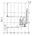
- FIG. 6 is a chart showing the difference in output waveform between the prior art circuit and the output circuit of the present invention by SPICE simulations.
- diodes D1 and D2 may be connected to the sources of a PMOS transistor M11 and an NMOS transistor M13, respectively, as shown in Fig. 2.
- a Schottky diode may be used.
- a transistor output circuit comprises a first insulated gate transistor having a control electrode connected to an input terminal, one main electrode connected to a first diode, and the other main electrode connected to a reference voltage source, and a second insulated gate transistor having a control electrode connected to the input terminal, one main electrode connected to an output terminal, and the other main electrode connected to the reference voltage source.
- a ratio (W 1 /L 1 ) of a gate width (W 1 ) to a gate length (L 1 ) of the first insulated gate transistor is larger than a ratio (W 2 /L 2 ) of a gate width (W 2 ) to a gate length (L 2 ) of the second insulated gate transistor.
Landscapes
- Physics & Mathematics (AREA)
- Engineering & Computer Science (AREA)
- Computer Hardware Design (AREA)
- Computing Systems (AREA)
- General Engineering & Computer Science (AREA)
- Mathematical Physics (AREA)
- Logic Circuits (AREA)
- Electronic Switches (AREA)
Abstract
Description
- The present invention relates to a transistor output circuit using an insulated gate transistor and, more particularly, to a transistor output circuit which prevents the oscillation (to be referred to as ringing hereinafter) of an output signal.
- Fig. 4 is a circuit diagram showing a prior art CMOS output circuit. Referring to Fig. 4, the CMOS output circuit includes a P-channel MOS transistor (to be referred to as a PMOS transistor hereinafter) M1, and an N-channel MOS transistor (to be referred to as an NMOS transistor hereinafter) M2. The source electrode, the drain electrode, and the gate electrode of the NMOS transistor M2 are connected to a
GND terminal 2, anoutput terminal 4, and an input terminal 3, respectively. The source electrode, the drain electrode, and the gate electrode of the PMOS transistor M1 are connected to apower supply 1, theoutput terminal 4, and the input terminal 3, respectively. Upon application of a logic level to the input terminal 3, the inverted logic level is output from theoutput terminal 4. - In recent years, a strong demand for driving a large capacitive load with a high-speed signal such as a video signal has arisen. To drive a large capacitive load by a CMOS output circuit, the output impedance of the CMOS output circuit must be lowered. For this purpose, the ratio (W/L) of the gate width (W) to the gate length (L) of each of the PMOS and NMOS transistors M1 and M2 must be increased.
- However, because of the parasitic inductance in the line from the output terminal to the capacitive load of the CMOS output circuit, or the power supply line of the CMOS output circuit, a closed circuit consisting of L, C, and R is equivalently formed, as shown in Fig. 5 (R equivalently represents the output impedance of the CMOS output circuit, L equivalently represents the inductance of the power supply (VDD) line or the line from the output terminal to the capacitive load, and C represents the capacitive load). For this reason, the output voltage waveform which appears in the capacitive load oscillates at a frequency f given by equation (1) below. Since Q of the oscillation is inversely proportional to R, the oscillation is harder to attenuate as the output impedance of the CMOS output circuit is lowered:

- When the capacitive load is to be driven at a high speed by the prior art CMOS output circuit, large ringing inevitably occurs, as described above.
- It is an object of the present invention to provide a CMOS output circuit which drives a capacitive load at a high speed and simultaneously minimizes ringing.
- In order to achieve the above object, according to the present invention, there is provided a transistor output circuit comprising:
- a first insulated gate transistor having a control electrode connected to an input terminal, one main electrode connected to an anode of a first diode, and the other main electrode connected to a reference voltage source; and
- a second insulated gate transistor having a control electrode connected to the input terminal, one main electrode connected to an output terminal, and the other main electrode connected to the reference voltage source,
- wherein a ratio (W1/L1) of a gate width (W1) to a gate length (L1) of the first insulated gate transistor is larger than a ratio (W2/L2) of a gate width (W2) to a gate length (L2) of the second insulated gate transistor.
-
- Fig. 1 is a circuit diagram showing a CMOS output circuit according to the first embodiment of the present invention and a load therein;
- Fig. 2 is a circuit diagram showing a CMOS output circuit according to the second embodiment of the present invention;
- Fig. 3 is a circuit diagram showing a CMOS output circuit according to the third embodiment in which Schottky diodes are used;
- Fig. 4 is a circuit diagram showing a prior art CMOS output circuit;
- Fig. 5 is an equivalent circuit diagram for explaining a load in the CMOS circuit; and
- Fig. 6 is a chart showing the drive voltage waveform of a capacitive load in the prior art CMOS output circuit and the drive voltage waveform of a capacitive load in the CMOS circuit according to the present invention.
- In the present application, a control electrode means the gate of an insulated gate transistor, and a main electrode means the source or drain of the insulated gate transistor.
- The function of the present invention will be described first. In the following description, a MOS transistor is used as an insulated gate transistor.
- In the present invention, when the output terminal level changes from the first level ("L" level) to the second level ("H" level), the first and second MOS transistors are turned on to flow a current to a capacitance as a load, thereby charging it. The ratio (W1/L1) of the gate width to the gate length of the first MOS transistor is larger than the ratio (W2/L2) of the gate width to the gate length of the second MOS transistor. In addition, the ON resistance of a MOS transistor is proportional to W/L, as represented by equation (2) below. Therefore, the capacitive load is charged at a high speed by the first MOS transistor having a large W/L value:

- To the contrary, when the output terminal level changes from the second level to the first level, the third and fourth MOS transistors are turned on to flow a current from the capacitance as a load, thereby performing a discharge operation. The ratio (W3/L3) of the gate width to the gate length of the third MOS transistor is larger than the ratio (W4/L4) of the gate width to the gate length of the fourth MOS transistor. In addition, the ON resistance of a MOS transistor is proportional to W/L, as described above. Therefore, the capacitive load is quickly discharged by the third MOS transistor having a large W/L value. When discharging continues, and the output terminal level reaches a certain value, the voltage VDS of the third MOS transistor is made close to zero by a diode which is series-connected to the third MOS transistor. Accordingly, the drain current decreases and finally becomes zero. On the other hand, the fourth MOS transistor is still in the ON state so that the subsequent discharging is performed by the fourth MOS transistor. In the fourth MOS transistor, the ratio (W4/L4) of the gate width to the gate length is smaller than W3/L3, the ON resistance is large, and Q by the parasitic inductance in the capacitive load connected to the output terminal or the connection line between the capacitive load and the output terminal becomes small, so ringing hardly occurs.
- The embodiments of the present invention will be described below.
- Fig. 1 is a circuit diagram that best shows the characteristic features of the present invention. Referring to Fig. 1, the CMOS output circuit includes a
power supply terminal 1, aGND terminal 2, an input terminal 3, anoutput terminal 4, and PMOS transistors M11 and M12. The ratio (W/L) of the gate width (W) to the gate length (L) of the PMOS transistor M11 is larger than that of the PMOS transistor M12. The CMOS output circuit also includes NMOS transistors M13 and M14. The ratio (W/L) of the gate width (W) to the gate length (L) of the NMOS transistor M13 is larger than that of the NMOS transistor M14. Aparasitic inductance 5 is present in the line from theoutput terminal 4 to a capacitive load 6. When the input terminal is at "L", the PMOS transistors M11 and M12 are in the ON state while the NMOS transistors M13 and M14 are in the OFF state, and the output terminal is at "H". When the input terminal goes "H", the PMOS transistors M11 and M12 are turned off, and the NMOS transistors M13 and M14 are turned on. The capacitive load 6 is discharged by the NMOS transistors M13 and M14, and the output terminal level drops. The ratio (W/L) of the gate width (W) to the gate length (L) of the NMOS transistor M13 is set to be larger than that of the NMOS transistor M14. The ON resistance of a MOS transistor is represented by the reciprocal of gm (mutual conductance), and gm in a saturated state is represented by the following equation:

- Cox is the gate oxide film capacitance,
- VGS is the gate-source voltage,
- Vt is the threshold voltage.
- When the output terminal level drops to the anode-cathode forward voltage (to be referred to as a voltage VF hereinafter; about 0.7 V) of a diode D2, the drain-source voltage (to be referred to as a voltage VDS hereinafter) of the NMOS transistor M13 almost becomes zero, so that the NMOS transistor M13 is turned off.
- At this time, the NMOS transistor M14 is kept in the ON state because the voltage VDS of the NMOS transistor M14 is held at about 0.7 V.
- Therefore, at output terminal levels lower than VF discharging is performed by the NMOS transistor M14. Since W/L of the NMOS transistor M14 is set to be small, its ON resistance is large, and discharging takes place slowly. At this time, because of the large ON resistance of the NMOS transistor M14, Q of the resonance caused by the
parasitic inductance 5 in the line and the capacitive load 6 is lowered. For this reason, ringing hardly occurs, and the attenuation of the ringing is slow. To increase the falling rate of the output terminal level, W/L of the NMOS transistor M13 may be increased. - This also applies to a case in which the input terminal level changes from "H" to "L", the NMOS transistors M13 and M14 are turned off while the PMOS transistors Mll and M12 are turned on, and the output terminal level changes from "L" to "H". Until the output terminal level reaches (power supply voltage - VF), the capacitive load is rapidly charged by the PMOS transistor M11 having a large value W/L. When the output terminal level reaches (power supply voltage - VF), the voltage VDS of the PMOS transistor M11 almost becomes zero and the PMOS transistor Mll is turned off. The subsequent charging for the capacitive load is slowly performed by the PMOS transistor M12 having a large ON resistance. In this case as well, Q of the resonant circuit is low, so ringing hardly occurs. Fig. 6 is a chart showing the difference in output waveform between the prior art circuit and the output circuit of the present invention by SPICE simulations.
- According to other embodiments of the present invention, diodes D1 and D2 may be connected to the sources of a PMOS transistor M11 and an NMOS transistor M13, respectively, as shown in Fig. 2. Alternatively, as shown in Fig. 3, a Schottky diode may be used.
- As has been described above, according to the present invention, when the capacitive load is to be driven by a transistor output circuit, a high-speed operation and ringing prevention can be simultaneously achieved.
- A transistor output circuit comprises a first insulated gate transistor having a control electrode connected to an input terminal, one main electrode connected to a first diode, and the other main electrode connected to a reference voltage source, and a second insulated gate transistor having a control electrode connected to the input terminal, one main electrode connected to an output terminal, and the other main electrode connected to the reference voltage source. A ratio (W1/L1) of a gate width (W1) to a gate length (L1) of the first insulated gate transistor is larger than a ratio (W2/L2) of a gate width (W2) to a gate length (L2) of the second insulated gate transistor.
Claims (13)
- A transistor output circuit comprising:a first insulated gate transistor having a control electrode connected to an input terminal, one main electrode connected to a first diode, and the other main electrode connected to a reference voltage source; anda second insulated gate transistor having a control electrode connected to said input terminal, one main electrode connected to an output terminal, and the other main electrode connected to said reference voltage source,wherein a ratio (W1/L1) of a gate width (W1) to a gate length (L1) of said first insulated gate transistor is larger than a ratio (W2/L2) of a gate width (W2) to a gate length (L2) of said second insulated gate transistor.
- A circuit according to claim 1, further comprising:a third insulated gate transistor having a control electrode connected to said input terminal, one main electrode connected to a second diode, and the other main electrode connected to a second reference voltage source which is different from said reference voltage source; anda fourth insulated gate transistor having a control electrode connected to said input terminal, one main electrode connected to said output terminal, and the other main electrode connected to said second reference voltage source,wherein a ratio (W3/L3) of a gate width (W3) to a gate length (L3) of said third insulated gate transistor is larger than a ratio (W4/L4) of a gate width (W4) to a gate length (L4) of said fourth insulated gate transistor.
- A circuit according to claim 1, wherein said first and second insulated gate transistors are transistors of the same conductivity type.
- A circuit according to claim 2, wherein said first insulated gate transistor is connected to an anode of said first diode.
- A circuit according to claim 1, wherein said first insulated gate transistor is connected to a cathode of said first diode.
- A circuit according to claim 2, wherein said third and fourth insulated gate transistors are transistors of the same conductivity type.
- A circuit according to claim 2, wherein said first and third insulated gate transistors are transistors of different conductivity type.
- A circuit according to any one of claims 2, 6, and 7, wherein said second and fourth insulated gate transistors are transistors of different conductivity type.
- A circuit according to claim 2, wherein said first and second diodes are connected in series with each other.
- A circuit according to claim 2, wherein one main electrode of said first insulated gate transistor is connected to that of said third insulated gate transistor.
- A transistor output circuit comprising:a first insulated gate transistor of a first conductivity type, which has a control electrode connected to an input terminal, one main electrode connected to an anode of a first diode, and the other main electrode connected to a first power supply;a second insulated gate transistor of the first conductivity type, which has a control electrode connected to said input terminal, one main electrode connected to an output terminal, and the other main electrode connected to said first power supply;a third insulated gate transistor of a second conductivity type, which has a control electrode connected to said input terminal, one main electrode connected to a cathode of a second diode, and the other main electrode connected to a second power supply having a voltage lower than that of said first power supply; anda fourth insulated gate transistor of the second conductivity type, which has a control electrode connected to said input terminal, one main electrode connected to said output terminal, and the other main electrode connected to said second power supply,wherein a cathode of said first diode and an anode of said second diode are connected to said output terminal, a ratio (W1/L1) of a gate width (W1) to a gate length (L1) of said first insulated gate transistor is larger than a ratio (W2/L2) of a gate width (W2) to a gate length (L2) of said second insulated gate transistor, and a ratio (W3/L3) of a gate width (W3) to a gate length (L3) of said third insulated gate transistor is larger than a ratio (W4/L4) of a gate width (W4) to a gate length (L4) of said fourth insulated gate transistor.
- A transistor output circuit comprising:a first insulated gate transistor of a first conductivity type, which has a control electrode connected to an input terminal, one main electrode connected to an output terminal, and the other main electrode connected to a cathode of a first diode;a second insulated gate transistor of the first conductivity type, which has a control electrode connected to said input terminal, one main electrode connected to said output terminal, and the other main electrode connected to a first power supply;a third insulated gate transistor of a second conductivity type, which has a control electrode connected to said input terminal, one main electrode connected to said output terminal, and the other main electrode connected to an anode of a second diode; anda fourth insulated gate transistor of the second conductivity type, which has a control electrode connected to said input terminal, one main electrode connected to said output terminal, and the other main electrode connected to a second power supply having a voltage lower than that of said first power supply,wherein an anode of said first diode is connected to said first power supply, a cathode of said second diode is connected to said second power supply, a ratio (W1/L1) of a gate width (W1) to a gate length (L1) of said first insulated gate transistor is larger than a ratio (W2/L2) of a gate width (W2) to a gate length (L2) of said second insulated gate transistor, and a ratio (W3/L3) of a gate width (W3) to a gate length (L3) of said third insulated gate transistor is larger than a ratio (W4/L4) of a gate width (W4) to a gate length (L4) of said fourth insulated gate transistor.
- A circuit according to claim 1 or 11, wherein said first and second diodes are Schottky diodes.
Applications Claiming Priority (2)
| Application Number | Priority Date | Filing Date | Title |
|---|---|---|---|
| JP8007323A JPH09200031A (en) | 1996-01-19 | 1996-01-19 | Complementary transistor output circuit |
| JP7323/96 | 1996-01-19 |
Publications (2)
| Publication Number | Publication Date |
|---|---|
| EP0785628A2 true EP0785628A2 (en) | 1997-07-23 |
| EP0785628A3 EP0785628A3 (en) | 1998-06-24 |
Family
ID=11662772
Family Applications (1)
| Application Number | Title | Priority Date | Filing Date |
|---|---|---|---|
| EP97100598A Withdrawn EP0785628A3 (en) | 1996-01-19 | 1997-01-16 | Transistor output circuit |
Country Status (3)
| Country | Link |
|---|---|
| US (1) | US5959473A (en) |
| EP (1) | EP0785628A3 (en) |
| JP (1) | JPH09200031A (en) |
Cited By (3)
| Publication number | Priority date | Publication date | Assignee | Title |
|---|---|---|---|---|
| WO2000065788A1 (en) * | 1999-04-26 | 2000-11-02 | Intel Corporation | Self-compensating output buffer |
| WO2001035532A1 (en) * | 1999-11-11 | 2001-05-17 | Infineon Technologies Ag | Integrated digital circuit and a method for operating same |
| DE102005050624A1 (en) * | 2005-10-21 | 2007-05-03 | Infineon Technologies Ag | Complementary metal oxide semiconductor buffer circuit e.g. inverter, for e.g. signal processing unit, has sections with conductivity types of transistors and connected to potential and control connections and transistors, respectively |
Families Citing this family (14)
| Publication number | Priority date | Publication date | Assignee | Title |
|---|---|---|---|---|
| DE19751651C1 (en) * | 1997-11-21 | 1999-02-18 | Bosch Gmbh Robert | Circuit for switching an inductive load |
| EP0969512B1 (en) * | 1998-06-30 | 2009-05-13 | Asulab S.A. | Inductive sensor |
| US6137317A (en) * | 1998-07-01 | 2000-10-24 | Intel Corporation | CMOS driver |
| US6184704B1 (en) * | 1999-02-08 | 2001-02-06 | Tritech Microelectronics | Design method for compensation of process variation in CMOS digital input circuits |
| DE19942688C2 (en) * | 1999-09-07 | 2001-11-29 | Siemens Ag | Method of operating an electronic circuit and electronic circuit |
| US6512401B2 (en) * | 1999-09-10 | 2003-01-28 | Intel Corporation | Output buffer for high and low voltage bus |
| US6351172B1 (en) * | 2000-02-29 | 2002-02-26 | Dmel Inc. | High-speed output driver with an impedance adjustment scheme |
| US7176739B2 (en) * | 2003-06-26 | 2007-02-13 | Lucent Technologies Inc. | Circuit to improve data bus performance |
| US6882187B1 (en) * | 2003-07-25 | 2005-04-19 | Silego Technology, Inc. | Line driving circuit |
| JP4313658B2 (en) * | 2003-11-28 | 2009-08-12 | 三菱電機株式会社 | Inverter circuit |
| US7511534B1 (en) * | 2007-10-05 | 2009-03-31 | Micron Technology, Inc. | Circuits, devices, systems, and methods of operation for a linear output driver |
| US8704550B2 (en) | 2007-11-29 | 2014-04-22 | Texas Instruments Incorporated | Architecture for VBUS pulsing in UDSM processes |
| KR100999137B1 (en) * | 2007-12-12 | 2010-12-08 | 현대자동차주식회사 | Car antenna |
| US12355448B2 (en) * | 2023-07-31 | 2025-07-08 | Dell Products L.P. | Slew rate in low-speed data communication interfaces |
Family Cites Families (9)
| Publication number | Priority date | Publication date | Assignee | Title |
|---|---|---|---|---|
| JPH0720205B2 (en) * | 1985-02-28 | 1995-03-06 | キヤノン株式会社 | Sync separation circuit |
| JP2779411B2 (en) * | 1985-03-01 | 1998-07-23 | キヤノン株式会社 | Switching device |
| JPH0732261B2 (en) * | 1985-04-11 | 1995-04-10 | キヤノン株式会社 | Semiconductor light receiving device |
| JPH0744416B2 (en) * | 1985-04-11 | 1995-05-15 | キヤノン株式会社 | Logarithmic compression circuit |
| JPH0681029B2 (en) * | 1985-12-27 | 1994-10-12 | 株式会社東芝 | Output circuit device |
| JPH04192717A (en) * | 1990-11-26 | 1992-07-10 | Mitsubishi Electric Corp | Mos transistor output circuit |
| US5274284A (en) * | 1991-01-24 | 1993-12-28 | Texas Instruments Incorporated | Output buffer circuits with controlled Miller effect capacitance |
| JP2930440B2 (en) * | 1991-04-15 | 1999-08-03 | 沖電気工業株式会社 | Semiconductor integrated circuit |
| US5168176A (en) * | 1991-07-23 | 1992-12-01 | Standard Microsystems Corporation | Apparatus and method to prevent the unsettling of a quiescent, low output channel caused by ground bounce induced by neighboring output channels |
-
1996
- 1996-01-19 JP JP8007323A patent/JPH09200031A/en active Pending
-
1997
- 1997-01-15 US US08/783,670 patent/US5959473A/en not_active Expired - Fee Related
- 1997-01-16 EP EP97100598A patent/EP0785628A3/en not_active Withdrawn
Cited By (8)
| Publication number | Priority date | Publication date | Assignee | Title |
|---|---|---|---|---|
| WO2000065788A1 (en) * | 1999-04-26 | 2000-11-02 | Intel Corporation | Self-compensating output buffer |
| GB2363534A (en) * | 1999-04-26 | 2001-12-19 | Intel Corp | Self-compensating output buffer |
| US6369604B1 (en) | 1999-04-26 | 2002-04-09 | Intel Corporation | Self-compensating output buffer |
| GB2363534B (en) * | 1999-04-26 | 2003-12-31 | Intel Corp | Self-compensating output buffer |
| DE10084448B4 (en) * | 1999-04-26 | 2007-02-15 | Intel Corporation, Santa Clara | Self-compensating output buffer |
| WO2001035532A1 (en) * | 1999-11-11 | 2001-05-17 | Infineon Technologies Ag | Integrated digital circuit and a method for operating same |
| DE102005050624A1 (en) * | 2005-10-21 | 2007-05-03 | Infineon Technologies Ag | Complementary metal oxide semiconductor buffer circuit e.g. inverter, for e.g. signal processing unit, has sections with conductivity types of transistors and connected to potential and control connections and transistors, respectively |
| DE102005050624B4 (en) * | 2005-10-21 | 2007-06-28 | Infineon Technologies Ag | CMOS buffer circuit and use thereof |
Also Published As
| Publication number | Publication date |
|---|---|
| JPH09200031A (en) | 1997-07-31 |
| US5959473A (en) | 1999-09-28 |
| EP0785628A3 (en) | 1998-06-24 |
Similar Documents
| Publication | Publication Date | Title |
|---|---|---|
| EP0785628A2 (en) | Transistor output circuit | |
| US6693469B2 (en) | Buffer interface architecture | |
| US4409501A (en) | Power-on reset circuit | |
| US5457420A (en) | Inverter circuit and level shifter circuit for providing a high voltage output | |
| EP0621694A2 (en) | Low power interface circuit | |
| US5546022A (en) | Static logic circuit with improved output signal levels | |
| EP2706664A2 (en) | Level shift device | |
| US20210135451A1 (en) | Integrated Circuit with Electrostatic Discharge Protection | |
| EP0351820B1 (en) | Output circuit | |
| JPH0626309B2 (en) | Output circuit | |
| US5218247A (en) | CMIS circuit and its driver | |
| US6853233B1 (en) | Level-shifting circuitry having “high” output impedance during disable mode | |
| EP0139833A2 (en) | CMOS transmission circuit | |
| US4352996A (en) | IGFET Clock generator circuit employing MOS boatstrap capacitive drive | |
| US6617903B2 (en) | Inverter circuit having an improved slew rate | |
| US5488326A (en) | Data output circuit for semiconductor integrated circuit device which prevents current flow from the output to supply voltage | |
| US20190081616A1 (en) | Input circuit | |
| HK1001534A (en) | Transistor output circuit | |
| US5369312A (en) | Hot carrier protection circuit | |
| US5994944A (en) | Level converting circuit having a high switching speed | |
| JP3518310B2 (en) | Capacitive load drive circuit | |
| US6501298B1 (en) | Level-shifting circuitry having “low” output during disable mode | |
| US5077492A (en) | Bicmos circuitry having a combination cmos gate and a bipolar transistor | |
| US6459300B1 (en) | Level-shifting circuitry having “high” output during disable mode | |
| JPH11243330A (en) | Input circuit |
Legal Events
| Date | Code | Title | Description |
|---|---|---|---|
| PUAI | Public reference made under article 153(3) epc to a published international application that has entered the european phase |
Free format text: ORIGINAL CODE: 0009012 |
|
| AK | Designated contracting states |
Kind code of ref document: A2 Designated state(s): DE FR GB |
|
| PUAL | Search report despatched |
Free format text: ORIGINAL CODE: 0009013 |
|
| AK | Designated contracting states |
Kind code of ref document: A3 Designated state(s): DE FR GB |
|
| 17P | Request for examination filed |
Effective date: 19981103 |
|
| 17Q | First examination report despatched |
Effective date: 20020717 |
|
| STAA | Information on the status of an ep patent application or granted ep patent |
Free format text: STATUS: THE APPLICATION IS DEEMED TO BE WITHDRAWN |
|
| 18D | Application deemed to be withdrawn |
Effective date: 20021128 |
|
| REG | Reference to a national code |
Ref country code: HK Ref legal event code: WD Ref document number: 1001534 Country of ref document: HK |