EP0785628A2 - Circuit de sortie de transistors - Google Patents
Circuit de sortie de transistors Download PDFInfo
- Publication number
- EP0785628A2 EP0785628A2 EP97100598A EP97100598A EP0785628A2 EP 0785628 A2 EP0785628 A2 EP 0785628A2 EP 97100598 A EP97100598 A EP 97100598A EP 97100598 A EP97100598 A EP 97100598A EP 0785628 A2 EP0785628 A2 EP 0785628A2
- Authority
- EP
- European Patent Office
- Prior art keywords
- electrode connected
- insulated gate
- transistor
- main electrode
- gate transistor
- Prior art date
- Legal status (The legal status is an assumption and is not a legal conclusion. Google has not performed a legal analysis and makes no representation as to the accuracy of the status listed.)
- Withdrawn
Links
- 238000010586 diagram Methods 0.000 description 7
- 239000008186 active pharmaceutical agent Substances 0.000 description 5
- 230000003071 parasitic effect Effects 0.000 description 5
- 238000007599 discharging Methods 0.000 description 4
- 230000007423 decrease Effects 0.000 description 3
- 230000010355 oscillation Effects 0.000 description 3
- 230000002265 prevention Effects 0.000 description 1
- 230000005855 radiation Effects 0.000 description 1
- 229920006395 saturated elastomer Polymers 0.000 description 1
- 238000004088 simulation Methods 0.000 description 1
- 235000013599 spices Nutrition 0.000 description 1
Images


Classifications
-
- H—ELECTRICITY
- H03—ELECTRONIC CIRCUITRY
- H03K—PULSE TECHNIQUE
- H03K19/00—Logic circuits, i.e. having at least two inputs acting on one output; Inverting circuits
- H03K19/003—Modifications for increasing the reliability for protection
- H03K19/00346—Modifications for eliminating interference or parasitic voltages or currents
- H03K19/00361—Modifications for eliminating interference or parasitic voltages or currents in field effect transistor circuits
-
- H—ELECTRICITY
- H03—ELECTRONIC CIRCUITRY
- H03K—PULSE TECHNIQUE
- H03K17/00—Electronic switching or gating, i.e. not by contact-making and –breaking
- H03K17/16—Modifications for eliminating interference voltages or currents
- H03K17/161—Modifications for eliminating interference voltages or currents in field-effect transistor switches
- H03K17/162—Modifications for eliminating interference voltages or currents in field-effect transistor switches without feedback from the output circuit to the control circuit
- H03K17/163—Soft switching
- H03K17/164—Soft switching using parallel switching arrangements
Definitions
- the present invention relates to a transistor output circuit using an insulated gate transistor and, more particularly, to a transistor output circuit which prevents the oscillation (to be referred to as ringing hereinafter) of an output signal.
- Fig. 4 is a circuit diagram showing a prior art CMOS output circuit.
- the CMOS output circuit includes a P-channel MOS transistor (to be referred to as a PMOS transistor hereinafter) M1, and an N-channel MOS transistor (to be referred to as an NMOS transistor hereinafter) M2.
- the source electrode, the drain electrode, and the gate electrode of the NMOS transistor M2 are connected to a GND terminal 2, an output terminal 4, and an input terminal 3, respectively.
- the source electrode, the drain electrode, and the gate electrode of the PMOS transistor M1 are connected to a power supply 1, the output terminal 4, and the input terminal 3, respectively.
- the inverted logic level is output from the output terminal 4.
- a transistor output circuit comprising:
- a control electrode means the gate of an insulated gate transistor
- a main electrode means the source or drain of the insulated gate transistor
- MOS transistor is used as an insulated gate transistor.
- the first and second MOS transistors are turned on to flow a current to a capacitance as a load, thereby charging it.
- the ratio (W 1 /L 1 ) of the gate width to the gate length of the first MOS transistor is larger than the ratio (W 2 /L 2 ) of the gate width to the gate length of the second MOS transistor.
- the ON resistance of a MOS transistor is proportional to W/L, as represented by equation (2) below.
- V DS the drain-source voltage
- the ratio (W 2 /L 2 ) of the gate width to the gate length is smaller than W 1 /L 1 , the ON resistance is large, and Q by a parasitic inductance in the capacitive load connected to the output terminal or the connection line between the capacitive load and the output terminal becomes small, so ringing hardly occurs.
- the third and fourth MOS transistors are turned on to flow a current from the capacitance as a load, thereby performing a discharge operation.
- the ratio (W 3 /L 3 ) of the gate width to the gate length of the third MOS transistor is larger than the ratio (W 4 /L 4 ) of the gate width to the gate length of the fourth MOS transistor.
- the ON resistance of a MOS transistor is proportional to W/L, as described above. Therefore, the capacitive load is quickly discharged by the third MOS transistor having a large W/L value.
- the voltage V DS of the third MOS transistor is made close to zero by a diode which is series-connected to the third MOS transistor. Accordingly, the drain current decreases and finally becomes zero.
- the fourth MOS transistor is still in the ON state so that the subsequent discharging is performed by the fourth MOS transistor.
- the ratio (W 4 /L 4 ) of the gate width to the gate length is smaller than W 3 /L 3 , the ON resistance is large, and Q by the parasitic inductance in the capacitive load connected to the output terminal or the connection line between the capacitive load and the output terminal becomes small, so ringing hardly occurs.
- Fig. 1 is a circuit diagram that best shows the characteristic features of the present invention.
- the CMOS output circuit includes a power supply terminal 1, a GND terminal 2, an input terminal 3, an output terminal 4, and PMOS transistors M11 and M12.
- the ratio (W/L) of the gate width (W) to the gate length (L) of the PMOS transistor M11 is larger than that of the PMOS transistor M12.
- the CMOS output circuit also includes NMOS transistors M13 and M14.
- the ratio (W/L) of the gate width (W) to the gate length (L) of the NMOS transistor M13 is larger than that of the NMOS transistor M14.
- a parasitic inductance 5 is present in the line from the output terminal 4 to a capacitive load 6.
- the PMOS transistors M11 and M12 are in the ON state while the NMOS transistors M13 and M14 are in the OFF state, and the output terminal is at "H”.
- the input terminal goes “H”
- the PMOS transistors M11 and M12 are turned off, and the NMOS transistors M13 and M14 are turned on.
- the capacitive load 6 is discharged by the NMOS transistors M13 and M14, and the output terminal level drops.
- the ratio (W/L) of the gate width (W) to the gate length (L) of the NMOS transistor M13 is set to be larger than that of the NMOS transistor M14.
- the drain-source voltage (to be referred to as a voltage V DS hereinafter) of the NMOS transistor M13 When the output terminal level drops to the anode-cathode forward voltage (to be referred to as a voltage V F hereinafter; about 0.7 V) of a diode D2, the drain-source voltage (to be referred to as a voltage V DS hereinafter) of the NMOS transistor M13 almost becomes zero, so that the NMOS transistor M13 is turned off.
- the NMOS transistor M14 is kept in the ON state because the voltage V DS of the NMOS transistor M14 is held at about 0.7 V.
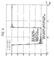
- FIG. 6 is a chart showing the difference in output waveform between the prior art circuit and the output circuit of the present invention by SPICE simulations.
- diodes D1 and D2 may be connected to the sources of a PMOS transistor M11 and an NMOS transistor M13, respectively, as shown in Fig. 2.
- a Schottky diode may be used.
- a transistor output circuit comprises a first insulated gate transistor having a control electrode connected to an input terminal, one main electrode connected to a first diode, and the other main electrode connected to a reference voltage source, and a second insulated gate transistor having a control electrode connected to the input terminal, one main electrode connected to an output terminal, and the other main electrode connected to the reference voltage source.
- a ratio (W 1 /L 1 ) of a gate width (W 1 ) to a gate length (L 1 ) of the first insulated gate transistor is larger than a ratio (W 2 /L 2 ) of a gate width (W 2 ) to a gate length (L 2 ) of the second insulated gate transistor.
Landscapes
- Physics & Mathematics (AREA)
- Engineering & Computer Science (AREA)
- Computer Hardware Design (AREA)
- Computing Systems (AREA)
- General Engineering & Computer Science (AREA)
- Mathematical Physics (AREA)
- Logic Circuits (AREA)
- Electronic Switches (AREA)
Applications Claiming Priority (2)
| Application Number | Priority Date | Filing Date | Title |
|---|---|---|---|
| JP8007323A JPH09200031A (ja) | 1996-01-19 | 1996-01-19 | 相補型トランジスタ出力回路 |
| JP7323/96 | 1996-01-19 |
Publications (2)
| Publication Number | Publication Date |
|---|---|
| EP0785628A2 true EP0785628A2 (fr) | 1997-07-23 |
| EP0785628A3 EP0785628A3 (fr) | 1998-06-24 |
Family
ID=11662772
Family Applications (1)
| Application Number | Title | Priority Date | Filing Date |
|---|---|---|---|
| EP97100598A Withdrawn EP0785628A3 (fr) | 1996-01-19 | 1997-01-16 | Circuit de sortie de transistors |
Country Status (3)
| Country | Link |
|---|---|
| US (1) | US5959473A (fr) |
| EP (1) | EP0785628A3 (fr) |
| JP (1) | JPH09200031A (fr) |
Cited By (3)
| Publication number | Priority date | Publication date | Assignee | Title |
|---|---|---|---|---|
| WO2000065788A1 (fr) * | 1999-04-26 | 2000-11-02 | Intel Corporation | Tampon de sortie auto-compensation |
| WO2001035532A1 (fr) * | 1999-11-11 | 2001-05-17 | Infineon Technologies Ag | Circuit numerique integre et procede pour le faire fonctionner |
| DE102005050624A1 (de) * | 2005-10-21 | 2007-05-03 | Infineon Technologies Ag | CMOS-Pufferschaltung und Verwendung derselben |
Families Citing this family (14)
| Publication number | Priority date | Publication date | Assignee | Title |
|---|---|---|---|---|
| DE19751651C1 (de) * | 1997-11-21 | 1999-02-18 | Bosch Gmbh Robert | Schaltungsanordnung zum Schalten einer induktiven Last |
| EP0969512B1 (fr) * | 1998-06-30 | 2009-05-13 | Asulab S.A. | Capteur inductif |
| US6137317A (en) * | 1998-07-01 | 2000-10-24 | Intel Corporation | CMOS driver |
| US6184704B1 (en) * | 1999-02-08 | 2001-02-06 | Tritech Microelectronics | Design method for compensation of process variation in CMOS digital input circuits |
| DE19942688C2 (de) * | 1999-09-07 | 2001-11-29 | Siemens Ag | Verfahren zum Betrieb einer elektronischen Schaltung und elektronische Schaltung |
| US6512401B2 (en) * | 1999-09-10 | 2003-01-28 | Intel Corporation | Output buffer for high and low voltage bus |
| US6351172B1 (en) * | 2000-02-29 | 2002-02-26 | Dmel Inc. | High-speed output driver with an impedance adjustment scheme |
| US7176739B2 (en) * | 2003-06-26 | 2007-02-13 | Lucent Technologies Inc. | Circuit to improve data bus performance |
| US6882187B1 (en) * | 2003-07-25 | 2005-04-19 | Silego Technology, Inc. | Line driving circuit |
| JP4313658B2 (ja) * | 2003-11-28 | 2009-08-12 | 三菱電機株式会社 | インバータ回路 |
| US7511534B1 (en) * | 2007-10-05 | 2009-03-31 | Micron Technology, Inc. | Circuits, devices, systems, and methods of operation for a linear output driver |
| US8704550B2 (en) | 2007-11-29 | 2014-04-22 | Texas Instruments Incorporated | Architecture for VBUS pulsing in UDSM processes |
| KR100999137B1 (ko) * | 2007-12-12 | 2010-12-08 | 현대자동차주식회사 | 차량용 안테나 |
| US12355448B2 (en) * | 2023-07-31 | 2025-07-08 | Dell Products L.P. | Slew rate in low-speed data communication interfaces |
Family Cites Families (9)
| Publication number | Priority date | Publication date | Assignee | Title |
|---|---|---|---|---|
| JPH0720205B2 (ja) * | 1985-02-28 | 1995-03-06 | キヤノン株式会社 | 同期分離回路 |
| JP2779411B2 (ja) * | 1985-03-01 | 1998-07-23 | キヤノン株式会社 | スイツチング装置 |
| JPH0732261B2 (ja) * | 1985-04-11 | 1995-04-10 | キヤノン株式会社 | 半導体受光装置 |
| JPH0744416B2 (ja) * | 1985-04-11 | 1995-05-15 | キヤノン株式会社 | 対数圧縮回路 |
| JPH0681029B2 (ja) * | 1985-12-27 | 1994-10-12 | 株式会社東芝 | 出力回路装置 |
| JPH04192717A (ja) * | 1990-11-26 | 1992-07-10 | Mitsubishi Electric Corp | Mosトランジスタ出力回路 |
| US5274284A (en) * | 1991-01-24 | 1993-12-28 | Texas Instruments Incorporated | Output buffer circuits with controlled Miller effect capacitance |
| JP2930440B2 (ja) * | 1991-04-15 | 1999-08-03 | 沖電気工業株式会社 | 半導体集積回路 |
| US5168176A (en) * | 1991-07-23 | 1992-12-01 | Standard Microsystems Corporation | Apparatus and method to prevent the unsettling of a quiescent, low output channel caused by ground bounce induced by neighboring output channels |
-
1996
- 1996-01-19 JP JP8007323A patent/JPH09200031A/ja active Pending
-
1997
- 1997-01-15 US US08/783,670 patent/US5959473A/en not_active Expired - Fee Related
- 1997-01-16 EP EP97100598A patent/EP0785628A3/fr not_active Withdrawn
Cited By (8)
| Publication number | Priority date | Publication date | Assignee | Title |
|---|---|---|---|---|
| WO2000065788A1 (fr) * | 1999-04-26 | 2000-11-02 | Intel Corporation | Tampon de sortie auto-compensation |
| GB2363534A (en) * | 1999-04-26 | 2001-12-19 | Intel Corp | Self-compensating output buffer |
| US6369604B1 (en) | 1999-04-26 | 2002-04-09 | Intel Corporation | Self-compensating output buffer |
| GB2363534B (en) * | 1999-04-26 | 2003-12-31 | Intel Corp | Self-compensating output buffer |
| DE10084448B4 (de) * | 1999-04-26 | 2007-02-15 | Intel Corporation, Santa Clara | Selbstkompensierender Ausgangspuffer |
| WO2001035532A1 (fr) * | 1999-11-11 | 2001-05-17 | Infineon Technologies Ag | Circuit numerique integre et procede pour le faire fonctionner |
| DE102005050624A1 (de) * | 2005-10-21 | 2007-05-03 | Infineon Technologies Ag | CMOS-Pufferschaltung und Verwendung derselben |
| DE102005050624B4 (de) * | 2005-10-21 | 2007-06-28 | Infineon Technologies Ag | CMOS-Pufferschaltung und Verwendung derselben |
Also Published As
| Publication number | Publication date |
|---|---|
| JPH09200031A (ja) | 1997-07-31 |
| US5959473A (en) | 1999-09-28 |
| EP0785628A3 (fr) | 1998-06-24 |
Similar Documents
| Publication | Publication Date | Title |
|---|---|---|
| EP0785628A2 (fr) | Circuit de sortie de transistors | |
| US6693469B2 (en) | Buffer interface architecture | |
| US4409501A (en) | Power-on reset circuit | |
| US5457420A (en) | Inverter circuit and level shifter circuit for providing a high voltage output | |
| EP0621694A2 (fr) | Circuit d'interface à faible consommation | |
| US5546022A (en) | Static logic circuit with improved output signal levels | |
| EP2706664A2 (fr) | Dispositif de décalage de niveau | |
| US20210135451A1 (en) | Integrated Circuit with Electrostatic Discharge Protection | |
| EP0351820B1 (fr) | Circuit de sortie | |
| JPH0626309B2 (ja) | 出力回路 | |
| US5218247A (en) | CMIS circuit and its driver | |
| US6853233B1 (en) | Level-shifting circuitry having “high” output impedance during disable mode | |
| EP0139833A2 (fr) | Circuit de transmission CMOS | |
| US4352996A (en) | IGFET Clock generator circuit employing MOS boatstrap capacitive drive | |
| US6617903B2 (en) | Inverter circuit having an improved slew rate | |
| US5488326A (en) | Data output circuit for semiconductor integrated circuit device which prevents current flow from the output to supply voltage | |
| US20190081616A1 (en) | Input circuit | |
| HK1001534A (en) | Transistor output circuit | |
| US5369312A (en) | Hot carrier protection circuit | |
| US5994944A (en) | Level converting circuit having a high switching speed | |
| JP3518310B2 (ja) | 容量性負荷駆動回路 | |
| US6501298B1 (en) | Level-shifting circuitry having “low” output during disable mode | |
| US5077492A (en) | Bicmos circuitry having a combination cmos gate and a bipolar transistor | |
| US6459300B1 (en) | Level-shifting circuitry having “high” output during disable mode | |
| JPH11243330A (ja) | 入力回路 |
Legal Events
| Date | Code | Title | Description |
|---|---|---|---|
| PUAI | Public reference made under article 153(3) epc to a published international application that has entered the european phase |
Free format text: ORIGINAL CODE: 0009012 |
|
| AK | Designated contracting states |
Kind code of ref document: A2 Designated state(s): DE FR GB |
|
| PUAL | Search report despatched |
Free format text: ORIGINAL CODE: 0009013 |
|
| AK | Designated contracting states |
Kind code of ref document: A3 Designated state(s): DE FR GB |
|
| 17P | Request for examination filed |
Effective date: 19981103 |
|
| 17Q | First examination report despatched |
Effective date: 20020717 |
|
| STAA | Information on the status of an ep patent application or granted ep patent |
Free format text: STATUS: THE APPLICATION IS DEEMED TO BE WITHDRAWN |
|
| 18D | Application deemed to be withdrawn |
Effective date: 20021128 |
|
| REG | Reference to a national code |
Ref country code: HK Ref legal event code: WD Ref document number: 1001534 Country of ref document: HK |