EP0786346A2 - Tintenstrahlaufzeichnungskopf - Google Patents
Tintenstrahlaufzeichnungskopf Download PDFInfo
- Publication number
- EP0786346A2 EP0786346A2 EP97101149A EP97101149A EP0786346A2 EP 0786346 A2 EP0786346 A2 EP 0786346A2 EP 97101149 A EP97101149 A EP 97101149A EP 97101149 A EP97101149 A EP 97101149A EP 0786346 A2 EP0786346 A2 EP 0786346A2
- Authority
- EP
- European Patent Office
- Prior art keywords
- ink
- plate
- recording head
- jet recording
- cavity
- Prior art date
- Legal status (The legal status is an assumption and is not a legal conclusion. Google has not performed a legal analysis and makes no representation as to the accuracy of the status listed.)
- Granted
Links
- 125000006850 spacer group Chemical group 0.000 claims description 40
- 239000000463 material Substances 0.000 claims description 32
- 239000000126 substance Substances 0.000 claims description 9
- 239000011295 pitch Substances 0.000 claims description 6
- 239000012790 adhesive layer Substances 0.000 claims description 5
- 238000004891 communication Methods 0.000 claims description 5
- 238000007789 sealing Methods 0.000 claims description 5
- 239000000853 adhesive Substances 0.000 claims 1
- 230000001070 adhesive effect Effects 0.000 claims 1
- WABPQHHGFIMREM-UHFFFAOYSA-N lead(0) Chemical compound [Pb] WABPQHHGFIMREM-UHFFFAOYSA-N 0.000 abstract description 3
- 239000010408 film Substances 0.000 description 47
- VYPSYNLAJGMNEJ-UHFFFAOYSA-N Silicium dioxide Chemical compound O=[Si]=O VYPSYNLAJGMNEJ-UHFFFAOYSA-N 0.000 description 26
- 239000000758 substrate Substances 0.000 description 26
- XUIMIQQOPSSXEZ-UHFFFAOYSA-N Silicon Chemical compound [Si] XUIMIQQOPSSXEZ-UHFFFAOYSA-N 0.000 description 24
- 229910052710 silicon Inorganic materials 0.000 description 24
- 239000010703 silicon Substances 0.000 description 24
- 239000010410 layer Substances 0.000 description 15
- 238000005530 etching Methods 0.000 description 14
- 239000000377 silicon dioxide Substances 0.000 description 13
- 235000012239 silicon dioxide Nutrition 0.000 description 13
- KRHYYFGTRYWZRS-UHFFFAOYSA-N Fluorane Chemical compound F KRHYYFGTRYWZRS-UHFFFAOYSA-N 0.000 description 8
- MCMNRKCIXSYSNV-UHFFFAOYSA-N Zirconium dioxide Chemical compound O=[Zr]=O MCMNRKCIXSYSNV-UHFFFAOYSA-N 0.000 description 8
- 238000004519 manufacturing process Methods 0.000 description 8
- 238000005192 partition Methods 0.000 description 8
- 230000003993 interaction Effects 0.000 description 6
- KWYUFKZDYYNOTN-UHFFFAOYSA-M Potassium hydroxide Chemical compound [OH-].[K+] KWYUFKZDYYNOTN-UHFFFAOYSA-M 0.000 description 5
- 239000002131 composite material Substances 0.000 description 5
- 239000012530 fluid Substances 0.000 description 5
- 238000000034 method Methods 0.000 description 5
- 230000002829 reductive effect Effects 0.000 description 5
- 230000002441 reversible effect Effects 0.000 description 5
- 229920002120 photoresistant polymer Polymers 0.000 description 4
- 238000003825 pressing Methods 0.000 description 4
- 238000004544 sputter deposition Methods 0.000 description 4
- 230000015572 biosynthetic process Effects 0.000 description 3
- BASFCYQUMIYNBI-UHFFFAOYSA-N platinum Chemical compound [Pt] BASFCYQUMIYNBI-UHFFFAOYSA-N 0.000 description 3
- 239000007788 liquid Substances 0.000 description 2
- 239000002861 polymer material Substances 0.000 description 2
- 230000002265 prevention Effects 0.000 description 2
- 230000001681 protective effect Effects 0.000 description 2
- 230000009467 reduction Effects 0.000 description 2
- 229910001220 stainless steel Inorganic materials 0.000 description 2
- 239000010935 stainless steel Substances 0.000 description 2
- DDFHBQSCUXNBSA-UHFFFAOYSA-N 5-(5-carboxythiophen-2-yl)thiophene-2-carboxylic acid Chemical compound S1C(C(=O)O)=CC=C1C1=CC=C(C(O)=O)S1 DDFHBQSCUXNBSA-UHFFFAOYSA-N 0.000 description 1
- 239000012670 alkaline solution Substances 0.000 description 1
- XAGFODPZIPBFFR-UHFFFAOYSA-N aluminium Chemical compound [Al] XAGFODPZIPBFFR-UHFFFAOYSA-N 0.000 description 1
- 229910052782 aluminium Inorganic materials 0.000 description 1
- 238000004140 cleaning Methods 0.000 description 1
- 238000005520 cutting process Methods 0.000 description 1
- 230000003247 decreasing effect Effects 0.000 description 1
- 230000001419 dependent effect Effects 0.000 description 1
- 238000006073 displacement reaction Methods 0.000 description 1
- 239000011810 insulating material Substances 0.000 description 1
- 238000010030 laminating Methods 0.000 description 1
- 230000000670 limiting effect Effects 0.000 description 1
- 239000000203 mixture Substances 0.000 description 1
- 230000003647 oxidation Effects 0.000 description 1
- 238000007254 oxidation reaction Methods 0.000 description 1
- 238000000059 patterning Methods 0.000 description 1
- 238000000206 photolithography Methods 0.000 description 1
- 239000002985 plastic film Substances 0.000 description 1
- 229910052697 platinum Inorganic materials 0.000 description 1
- 238000002360 preparation method Methods 0.000 description 1
- 239000010409 thin film Substances 0.000 description 1
Images



Classifications
-
- B—PERFORMING OPERATIONS; TRANSPORTING
- B41—PRINTING; LINING MACHINES; TYPEWRITERS; STAMPS
- B41J—TYPEWRITERS; SELECTIVE PRINTING MECHANISMS, i.e. MECHANISMS PRINTING OTHERWISE THAN FROM A FORME; CORRECTION OF TYPOGRAPHICAL ERRORS
- B41J2/00—Typewriters or selective printing mechanisms characterised by the printing or marking process for which they are designed
- B41J2/005—Typewriters or selective printing mechanisms characterised by the printing or marking process for which they are designed characterised by bringing liquid or particles selectively into contact with a printing material
- B41J2/01—Ink jet
- B41J2/015—Ink jet characterised by the jet generation process
- B41J2/04—Ink jet characterised by the jet generation process generating single droplets or particles on demand
- B41J2/045—Ink jet characterised by the jet generation process generating single droplets or particles on demand by pressure, e.g. electromechanical transducers
- B41J2/055—Devices for absorbing or preventing back-pressure
-
- B—PERFORMING OPERATIONS; TRANSPORTING
- B41—PRINTING; LINING MACHINES; TYPEWRITERS; STAMPS
- B41J—TYPEWRITERS; SELECTIVE PRINTING MECHANISMS, i.e. MECHANISMS PRINTING OTHERWISE THAN FROM A FORME; CORRECTION OF TYPOGRAPHICAL ERRORS
- B41J2/00—Typewriters or selective printing mechanisms characterised by the printing or marking process for which they are designed
- B41J2/005—Typewriters or selective printing mechanisms characterised by the printing or marking process for which they are designed characterised by bringing liquid or particles selectively into contact with a printing material
- B41J2/01—Ink jet
- B41J2/135—Nozzles
- B41J2/14—Structure thereof only for on-demand ink jet heads
- B41J2/14201—Structure of print heads with piezoelectric elements
- B41J2/14233—Structure of print heads with piezoelectric elements of film type, deformed by bending and disposed on a diaphragm
-
- B—PERFORMING OPERATIONS; TRANSPORTING
- B41—PRINTING; LINING MACHINES; TYPEWRITERS; STAMPS
- B41J—TYPEWRITERS; SELECTIVE PRINTING MECHANISMS, i.e. MECHANISMS PRINTING OTHERWISE THAN FROM A FORME; CORRECTION OF TYPOGRAPHICAL ERRORS
- B41J2/00—Typewriters or selective printing mechanisms characterised by the printing or marking process for which they are designed
- B41J2/005—Typewriters or selective printing mechanisms characterised by the printing or marking process for which they are designed characterised by bringing liquid or particles selectively into contact with a printing material
- B41J2/01—Ink jet
- B41J2/135—Nozzles
- B41J2/14—Structure thereof only for on-demand ink jet heads
- B41J2002/14387—Front shooter
-
- B—PERFORMING OPERATIONS; TRANSPORTING
- B41—PRINTING; LINING MACHINES; TYPEWRITERS; STAMPS
- B41J—TYPEWRITERS; SELECTIVE PRINTING MECHANISMS, i.e. MECHANISMS PRINTING OTHERWISE THAN FROM A FORME; CORRECTION OF TYPOGRAPHICAL ERRORS
- B41J2/00—Typewriters or selective printing mechanisms characterised by the printing or marking process for which they are designed
- B41J2/005—Typewriters or selective printing mechanisms characterised by the printing or marking process for which they are designed characterised by bringing liquid or particles selectively into contact with a printing material
- B41J2/01—Ink jet
- B41J2/135—Nozzles
- B41J2/14—Structure thereof only for on-demand ink jet heads
- B41J2002/14419—Manifold
Definitions
- the present invention relates to an ink-jet recording head.
- An ink-jet recording head is a device which records an image on recording paper by pressurizing an ink cavity filled with ink so as to jet ink from a nozzle orifice (or an opening).
- a spacer which constitutes a space for pressurizing ink to eject ink droplets, or an ink flow path such as a so-called ink cavity, is formed by anisotropic etching.
- anisotropic etching operation a silicon monocrystalline substrate is etched using an alkaline liquid, so that the difference in etch rates in the crystallographic axis is utilized.
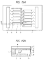
- Figs. 15A and 15B show one example of an ink-jet recording head which uses a spacer S formed by anisotropically etching a silicon monocrystalline substrate.
- a plurality of substantially-rectangular ink cavities A are formed in the spacer S on constant pitches in the direction of a shorter side of the cavity.
- the ink cavity A is connected at one end to an ink reservoir C via an ink supply port B.
- a nozzle orifice D for ejecting ink is formed in the other end of each ink cavity A.
- a resilient plate E is fitted to one side of the spacer S of the recording head that has flow paths such as the ink cavities A formed therein. Further, a nozzle plate G having the nozzle orifices D formed therein is fitted to the other side of the spacer S.
- a drive signal is fed to these electrodes from outside via an electrically conductive pattern L formed on the surface of the resilient plate E.
- a terminal for receiving a flexible cable which connects the electrically conductive pattern L to an external drive circuit, is usually provided along one end of the recording head.
- ink other than the ink ejected from the nozzle orifices D reversely flows to the ink reservoir C from the ink supply ports B if the plurality of ink cavities A are pressurized. If a large quantity of ink reversely flows to the ink reservoir C, the pressure of the ink reservoir C will increase, thereby resulting in the ink flowing into the unpressurized ink cavities A. As a result, ink droplets will be ejected from the nozzle orifices D of the unpressurized ink cavities A. Such interaction arising between adjacent ink reservoirs (cross-stroke) is not a desirable phenomenon in the ink-jet recording head.
- the area of the resilient plate corresponding to the ink reservoir C, i.e., the thin portion M, is deformed as a result of exertion of the negative pressure generated when the ink is introduced.
- the lower electrode M, the piezoelectric film J, and the upper electrode K stacked on the resilient plate E also experience large stress, and hence they are significantly deformed, which in turn results in the upper electrode K becoming apt to break.
- the present invention intends to overcome the above problems.
- the object is solved by the ink-jet recording head according to independent claims 1 and 13.
- the present invention generally relates to the structure of an ink reservoir for supplying ink to an ink cavity which generates pressure for use in ejecting ink droplets.
- an ink-jet recording head which is capable of preventing break in a line while reducing interaction to as small as possible.
- an ink-jet recording head comprising: a nozzle plate having a plurality of nozzle orifices formed therein for ejecting ink in the form of an ink droplet; a spacer made comprising, substantially-rectangular ink cavities for pressurizing ink which are respectively connected to the nozzle orifices and are arrayed on constant pitches in the direction of a shorter side of the ink cavity, ink supply ports connected to the respective ink cavities for supplying ink, and an ink reservoir connected to the ink supply ports for supplying ink to the plurality of ink cavities, wherein the nozzle plate seal one surface of the spacer; a resilient plate sealing the other side of the spacer and brings about variations in the pressure of the ink cavity; a piezoelectric substance formed on the surface of the resilient plate; upper electrodes formed so as to respectively correspond to the ink cavities in order to apply a signal to the piezoelectric substance; a thin portion which is elastically deformable when
- a thin portion 13 which becomes resiliently deformed by the ink reversely flowed from an ink cavity 2 is provided in the area of a compliance plate facing an ink reservoir 4.
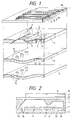
- Figs. 1 and 2 show one embodiment of an ink-jet recording head of the present invention.
- reference numeral 1 designates a spacer.
- Ink cavities 2, ink supply ports 3, and ink reservoirs 4 are formed by anisotropically etching a silicon monocrystalline substrate.
- the ink cavities 2 are formed in the form of through-holes, and the ink supply ports 3 and the ink reservoirs 4 are formed in the form of recesses having their openings facing towards a nozzle plate 5 which will be described later.
- the ink supply ports 3 can be provided with fluid resistance necessary to eject ink droplets.
- the rigidity of the area of a resilient plate 7 corresponding to the ink reservoir 4 is increased by forming a thin portion 6.
- a lead electrode 16 which is to be formed in that area and will be described later, is prevented from becoming deformed.
- Reference numeral 7 designates the previously-described resilient plate for sealing one side of the spacer 1.
- a lower electrode 8, a piezoelectric film 9, and an upper electrode 10 are formed in that order on the resilient plate.
- a compliance plate 11 is interposed between one side of the spacer 1 and the nozzle plate 5 which will be described later.
- a thin portion 13 is formed in the compliance plate so as to correspond to the ink reservoir 4, and the thin portion 13 has a recess 12 facing toward the nozzle plate 5.
- the nozzle orifices 14 are formed in the nozzle plate on constant pitches such that each nozzle orifice 14 is connected to one end of the ink cavity 2.
- the nozzle plate 5 is brought into close contact with the compliance plate 11.
- the recess 12 of the compliance plate 11 By virtue of the recess 12 of the compliance plate 11, a space is formed which permits deformation of the thin portion 13 of the compliance plate 11.
- a silicon monocrystalline substrate having a thickness of about 150 to 300 ⁇ m (micrometers) is usually used as the silicon monocrystalline substrate forming the spacer 1.
- a silicon monocrstyalline substrate having a thickness of about 180 to 280 ⁇ m is desirable, and preferably about 220 ⁇ m.
- the thickness of the silicon monocrystalline substrate depends on the cost of the silicon monocrystalline substrate and the fact that the ink reservoirs 4 are usually arrayed at densities of 180 - 360 reservoirs per inch.
- the rigidity of the partition wall is increased by reducing the thickness of the silicon monocrystalline substrate, it is necessary to obtain a quite thin wafer of a silicon monocrystalline substrate. If a silicon monocrystalline ingot having a large diameter is sliced into thin substrates, a cutting margin will form an increasingly proportion of the entire area of the substrate. Further, an accuracy of slicing also becomes decreased. Therefore, a precise slicing operation becomes necessary, which in turn results in increased costs. In view of these circumstances, it is desirable to use a silicon monocrystalline substrate having a thickness of 180 to 280 ⁇ m and, more particularly, to use a silicon monocrystalline substrate having a thickness of 220 ⁇ m in order to reduce the cost of a silicon monocrystalline substrate.
- the ink cavities 2 are required to have a high density in the direction in which they are arranged, it is necessary to form the ink cavity such that the surfaces of the ink cavity 2 in its longitudinal direction become (111) planes perpendicular to the (110) plane.
- a shorter-side surface of the ink cavity 2 forms an angle of about 70 degrees with respect to the (111) plane in the longitudinal direction of the cavity and comes about as a (111) plane perpendicular to the (110) plane.
- the nozzle orifice 14 is tapered, thereby contributing to prevention of settlement of the ink.
- the spacer is formed by anisotropically etching the silicon monocrystalline substrate, there will be another advantage of making it possible to integrally form the resilient plate 7, the lower electrode 8, the piezoelectric film 9, and the upper electrode 10 through processes by using a film forming technique in combination with anisotropic etching, in addition to the advantage of allowing high-density layout of the ink cavities 2.
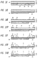
- Figs. 3I to 3VII and 3I' to 3VII' show one embodiment in which a spacer, a resilient plate, a lower electrode, a piezoelectric film, and an upper electrode are formed through a sequence of processes.
- Figs. 3I to 3VII are longitudinal cross-sectional views of the ink cavity
- Figs. 3I' to 3VII' are transverse cross-sectional views of the ink cavity.
- a base material 22 is prepared by forming a silicon dioxide layer 21 to a thickness of about 1 micrometer on the entire surface of a silicon monocrystalline substrate 20 having its surface sliced in a (110) orientation, using thermal oxidation or the like.
- the silicon dioxide layer 21 serves as an etching protection film when the silicon monocrystalline substrate 20 is etched as well as serving as an insulating film of a drive section to be formed on the base material.
- a zirconia (Zr) film is formed on the surface of the silicon dioxide layer 21 by sputtering.
- the zirconia film is thermally oxidized to form a resilient film 23 which consists of zirconia having a thickness of 0.8 ⁇ m.
- the resilient film 23 made of zirconia has a high Young's modulus and is capable of converting the distortion of the piezoelectric film 25, which will be described later, to flexible displacements with high efficiency.
- a platinum (Pt) film is formed on the surface of the resilient film 23 to a thickness of about 0.2 ⁇ m by sputtering, so that a lower electrode 24 is formed.
- Piezoelectric material such as PZT is formed on the surface of the lower electrode to a thickness of 1 micrometer by sputtering or the like, so that a piezoelectric film 25 is formed.
- An upper electrode 27 is formed from aluminum (Al) on the surface of the piezoelectric film to a thickness of 0.2 ⁇ m by sputtering or the like (I).
- the upper electrode 27, the piezoelectric film 25, and the lower electrode 24 are patterned so as to correspond to the layout of the ink cavities 2, and the substrate is cut into piezoelectric elements.
- the upper electrode 27 When being patterned, the upper electrode 27 is independently drawn so as to correspond to each ink cavity 2, whereby it doubles as a lead wire which connects the piezoelectric element to the drive circuit (II).
- Photoresists 28 and 29 are formed such that the ink cavities 2 are oriented in the direction of a lattice of a ⁇ -1 -1 -2 ⁇ zone axis parallel to (1 -1 -1) and (110) zone planes or in the direction of a lattice ⁇ 112 ⁇ equivalent to the zone axis (III).
- the silicon dioxide layer 21 is removed by use of a buffer hydrofluoric acid fluid composed of a mixture of hydrofluoric acid and ammonium fluoride in proportions of 1:6. As a result, a window 31 for anisotropic etching purposes is patterned.
- the photoresist 29 on the silicon dioxide layer in the area where the ink supply port 3 is to be formed is again exposed to light, and the thus-exposed photoresist is developed. Subsequent to such a so-called multi-exposure process, the silicon dioxide layer is half-etched by use of the previously-described buffer hydrofluoric acid fluid for about five min. such that the thickness of the silicon dioxide layer below the photoresist layer 29 is reduced to about 0.5 ⁇ m (IV).
- the base material 22 is immersed in a 10% potassium hydroxide solution heated up to about 80°C (degrees centigrade), whereby the base material is anisotropically etched.
- the silicon dioxide layers 21 and 21' which acted as the protective film against anisotropic etching are also gradually dissolved and are etched away by a thickness of about 0.4 ⁇ m.
- the silicon dioxide layer 21' in the area where the ink supply port 3 is to be formed is reduced to a thickness of about 0.1 ⁇ m, whereas the silicon dioxide layer 21 in the other area is reduced to a thickness of about 0.6 ⁇ m (V).
- the base material 22 is immersed in the buffer hydrofluoric acid fluid for the period during which the silicon dioxide layer having a thickness of 0.1 ⁇ m can be removed; e.g., about one minute.
- the silicon dioxide layer 21' in the area where the ink supply port 3 is to be formed is removed, whereas the silicon dioxide film 21 in the other area is left as a layer 21'' having a thickness of about 0.5 ⁇ m (VI).
- the base material 22 is anisotropically etched so as to selectively etch the area of the ink supply port 3 again by immersing it in a potassium hydroxide solution of about 40%. As a result, the thickness of the area of the ink supply port 3 is reduced, so that a recess having fluid resistance required by the ink supply port 3 is formed (VII).
- the piezoelectric film 24 is separated after having been patterned so as to be identical with the upper electrodes 10. Only the area of the piezoelectric film 24 where the upper electrode 10 and the lower electrode 8 overlap becomes displaced, and hence the above-described patterning of the piezoelectric film 24 does not become absolutely necessary.
- a lead electrode 16 is provided, as shown in Fig. 1.
- the lead electrode 16 is formed so as to extend to the end of the recording head while the piezoelectric film 9 acts as an insulating film between the upper electrode 10 and the lower electrode 8.
- the piezoelectric film is a ferroelectric substance having a dielectric constant of about 800 to 3000. Therefore the electrostatic capacitance of the lead electrode 16 becomes large, thereby resulting in increased charging current and dielectric loss. For this reason, it is desirable to form the lower electrode 8 from an insulating material other than a piezoelectric material and to use that lower electrode as an insulating film.
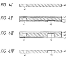
- a through hole 41 is formed in a plate material 40 such as stainless steel by pressing (I), and a dry film 42 which is a photosensitive plastic sheet is bonded to both sides of the plate material 40 by laminating or the like.
- the area of one dry film 42 where the thin portion 13 is to be formed is exposed and developed so as to be removed, whereby a window 43 for etching purposes is formed (II).
- a recess is formed to a predetermined depth by use of a liquid suitable for use in etching the plate material 40 in a time controlled manner, whereby the thin portion 13 is formed (III).
- a compliance plate is finished by removing the dry films 42, 42 after the etching operation has been completed (IV).
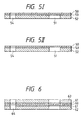
- Figs. 5I and 5II show another embodiment of the compliance plate 11 of the ink-jet recording head of the present invention.
- a first plate material 50 which is formed from stainless steel or the like to a thickness suitable for the thin portion 13 is stacked on a second plate material 52 which has the same thickness as the depth of the recess 12 and has a through hole 51 previously formed in its area to be formed into the thin portion 13. They are bonded together while a dry film 53 sandwiched between them. Then, a through hole 54 is formed in the area of the thus-formed laminate corresponding to the through hole 15 (I). The uncovered dry film 53 in the through hole 51 is removed by photolithography, as required (II).
- the present embodiment it is possible to control the thickness of the thin portion 13 with the same roll accuracy as that with which the first plate material 50 is formed. It is easy to control the thickness of the thin portion by controlling the etching time. Further, it is possible to form a thin portion with high accuracy.
- the recess facing the thin portion is formed by pressing the second plate material 52 in the previously-described embodiment.
- a window of an etching protective film is formed in the area of the second plate material 52 which is to become the recess 12, as previously described with reference to Figs. 4I to 4IV.
- the second plate is etched only as far as the dry film 53.
- the recess is formed only in one side of the compliance plate in the foregoing embodiment. Both sides of the first plate material 60 are coated with dry films 61, 61, as shown in Fig. 6. Then, second plate materials 62, 63 are respectively stacked on the dry films. Through holes 64 are formed in the areas corresponding to the communication holes 15 by pressing. In contrast, the areas of the second plate materials 62, 63 which are to be opposite to the recess, are etched. Further, through holes are previously formed in the area of the second plate materials 62 and 63 corresponding to the recess 12 by pressing, whereby it is possible to manufacture the compliance plate which acts as the thin portion 13 with the first plate material 60 between the second plate materials, with high accuracy. According to the present embodiment, the volume of the ink reservoir can be increased, and a silicon monocrystalline substrate for use as a spacer can be thinly formed.
- the piezoelectric film 9 sandwiched between the electrodes is deflected such that the ink cavity 2 becomes concave, whereby the ink cavity 2 expands.
- the ink stored in the ink reservoir 4 flows into the ink cavity 2 through the ink supply port 3.
- the piezoelectric film 9 If electric charges on the piezoelectric film 9 are discharged after a predetermined period of time has elapsed, the piezoelectric film 9 returns to its original state, whereby the ink cavity 2 is compressed. As a result, the ink of the ink cavity 2 is pressurized, and a part of the ink is ejected from the nozzle orifice 14 in the form of ink droplets, so that dots are formed on a recording medium. Further, some of the ink reversely flows to the ink reservoir 4 through the ink supply port 3.
- the ink flowing into the ink reservoir 4 temporarily increases the pressure of the ink reservoir 4.
- the thin portion 13 of the compliance plate 11 is deflected such that the recess formed between the compliance plate and the nozzle orifice 5 becomes convex, whereby the volume of the ink reservoir 4 is increased.
- the pressure of the ink reservoir 4 drops.
- the quantity of the ink reversely flows into the ink cavity 2 through the ink supply port 3 is suppressed, and hence printing is carried out without interaction. If the pressure of the ink reservoir 4 drops as a result of attenuation after a predetermined period of time has elapsed, the thin portion 13 returns to its original state by virtue of its resilience.
- the nozzle orifices 14 are sealed with capping members (not shown) for replacement of an ink tank, and a negative pressure is exerted on the ink tank.
- a measured amount of ink is discharged from the ink tank through the nozzle orifice 14 via the ink reservoir 4 and the ink cavity 2.
- the thin portion 13 of the compliance plate 11 becomes resiliently deformed first, so that the pressure is balanced. As a result, it is possible to suppress the deformation of the lead electrode 16 of the resilient plate 7 to a small degree.
- a compliance value of the thin portion 13 is absolutely necessary for a compliance value of the thin portion 13 to be greater than all the compliance values of the plurality of ink cavities 2 by more than a constant value.
- the pressure Pr and the variation AVr are proportional to each other according to a proportional constant Cr.
- This proportional constant Cr represents the compliance value of the thin portion 13.
- a proportional coefficient Cc between the pressure Pr and the variation AVr obtained when a certain pressure is applied to a composite film which is provided on the ink cavity 2 and is composed of the resilient plate 7, the lower electrode 8, the piezoelectric film 9, and the upper electrode 10, represents the compliance value of the ink cavity 2.
- the compliance value Cc of the composite film does not represent all the compliance values of the ink cavity 2.
- the partition wall between the ink cavities 2, or others also contributes to the compliance of the ink cavity.
- the compliance value of the composite film is several to ten times larger than the compliance values of other areas, e.g., the partition walls. Therefore, it is possible to say that the compliance value of the ink cavity 2 is substantially the compliance value Cc of the composite film composed of the resilient plate 7, the lower electrode 8, the piezoelectric film 9, and the upper electrode 10.
- the inventor of the present invention found that it was only necessary to establish the following relationship between the compliance value Cr of the thin portion 13, the number of ink cavities 2 "n,” and the compliance value Cc of the composite film Cr in order to effectively reduce the pressure of the ink reservoir 4; namely, Cr > 8 x n x Cc .
- the thickness of the thin portion 13 of the compliance plate 11 is designed so as to satisfy the above-described expression, whereby prevention of interaction is ensured, and an ink-jet recording head having a high print quality can be formed.
- the recess 12 is formed in the side of the compliance plate 11 facing the nozzle plate 5, and the thin portion 13 is formed in the side of the compliance plate facing the ink reservoir 4 in the previously-described embodiment.
- a recess 70 in the area of the side of the nozzle plate 5 opposite to the ink reservoir 4 so as to be open toward the ink reservoir, as shown in Fig. 7.
- a thin portion 71 which provides a recess toward the ink reservoir, at least in the area of the compliance plate 11 opposite to the recess 70.
- the volume of the ink reservoir 4 can be compensated for by means of the compliance plate 11.
- a thin silicon monocrystalline substrate can be used for the spacer 1, and the entire width of the recording head can be reduced.
- reference numeral 78 designates a communication hole which connects the nozzle orifice 14 to an ink cavity 79 of the spacer 77.
- the present embodiment it is possible to reduce the area of the silicon monocrystalline substrate forming the spacer 77 by at least the area corresponding to the ink reservoir, thereby resulting in reductions in costs. Further, the rigidity of the spacer can be accordingly increased only by removal of the ink reservoir having a comparatively large opening. It is possible to facilitate handling of the spacer during assembly processes.
- Fig. 10 shows another embodiment of the present invention.
- reference numeral 80 designates a nozzle plate.
- a thin portion 83 is formed in the area of a spacer 81 opposite to an ink reservoir 82 in such a way as to provide a recess in the exterior of the nozzle plate.
- the recess is filled with material which is easy to resiliently deform and to fill; e.g., a high polymer material 84, such that the overall nozzle plate becomes flat, as required.
- reference numeral 85 designates a nozzle orifice.
- the thin portion 83 of the nozzle plate 80 expands to the outside, whereby pressure is absorbed. Vibrations are effectively absorbed by means of viscous elasticity of the high polymer material 84 filling the thin portion 83. Further, in a case where the nozzle orifice is abraded by an elastic plate such as rubber at the time of a cleaning operation, the ink-jet recording head can smoothly travel without the recess being caught by the resilient plate.
- the same operation as that carried out by the ink reservoir 82 can be realized by forming a recess in the area of a head holder 85 for supporting a head which corresponds to the ink reservoir, and by forming an ink reservoir 86 by means of combination of the spacer 81 and the head holder 85, as shown in Fig. 11.
- the ink reservoir 86 is formed by utilization of the head holder 85, formation of a space 87 with respect to the head holder can be ensured, as shown in Fig. 12. Further, the same operation that carried out by the ink reservoir can be attained by fitting a cup member 88, which is resiliently deformable as a result of an increase in the pressure of the ink reservoir 86, to the wall surface of the head holder 85 in a fluid-tight manner, by forming a recess 85a in the interior of the head holder 85 as shown in Fig. 13, and by sealing the recess 85a in a fluid-tight manner using a plate material 89 which is resiliently deformable as a result of an increase in the pressure of the ink reservoir 86 at the time of a printing operation.
- the thin portion is formed in the area of the ink reservoir opposite to the nozzle plate in the previously-described embodiment.
- an ink reservoir 91 of a spacer 90 as a through hole, as shown in Fig. 14.
- the area of a resilient plate 92 opposite to the ink reservoir 91 is made deformable as a result of an increase in the pressure of the ink reservoir 91 at the time of a printing operation.
- the lead area of the lower and upper electrodes may be provided on the nozzle plate.
- an ink-jet recording head includes a nozzle plate which has a plurality of nozzle orifices formed therein for ejecting ink in the form of an ink droplet and seals one surface of a spacer; the spacer made up of substantially-rectangular ink cavities for pressurizing ink which are respectively connected to the nozzle orifices and are arrayed on constant pitches in the direction of a shorter side of the ink cavity, ink supply ports connected to the respective ink cavities for supplying ink, and an ink reservoir connected to the ink supply ports for supplying ink to the plurality of ink cavities; a resilient plate which seals the other side of the spacer and brings about variations in the pressure of the ink cavity; a piezoelectric substance formed on the surface of the resilient plate; and upper electrodes formed so as to respectively correspond to the ink cavities in order to apply a signal to the piezoelectric substance.
- a thin portion which is elastically deformable when being subjected to the ink reversely flowed from the ink cavity is formed at least in either the area of the nozzle plate being opposite to the ink reservoir or in the interior of the ink reservoir.
Landscapes
- Particle Formation And Scattering Control In Inkjet Printers (AREA)
- Ink Jet (AREA)
Applications Claiming Priority (9)
| Application Number | Priority Date | Filing Date | Title |
|---|---|---|---|
| JP12115/96 | 1996-01-26 | ||
| JP1211596 | 1996-01-26 | ||
| JP1211596 | 1996-01-26 | ||
| JP7189296 | 1996-03-27 | ||
| JP71892/96 | 1996-03-27 | ||
| JP7189296 | 1996-03-27 | ||
| JP191484/96 | 1996-07-02 | ||
| JP19148496 | 1996-07-02 | ||
| JP19148496A JP3402349B2 (ja) | 1996-01-26 | 1996-07-02 | インクジェット式記録ヘッド |
Publications (3)
| Publication Number | Publication Date |
|---|---|
| EP0786346A2 true EP0786346A2 (de) | 1997-07-30 |
| EP0786346A3 EP0786346A3 (de) | 1998-03-18 |
| EP0786346B1 EP0786346B1 (de) | 2002-12-18 |
Family
ID=27279708
Family Applications (1)
| Application Number | Title | Priority Date | Filing Date |
|---|---|---|---|
| EP97101149A Expired - Lifetime EP0786346B1 (de) | 1996-01-26 | 1997-01-24 | Tintenstrahlaufzeichnungskopf |
Country Status (4)
| Country | Link |
|---|---|
| US (2) | US6193360B1 (de) |
| EP (1) | EP0786346B1 (de) |
| JP (1) | JP3402349B2 (de) |
| DE (1) | DE69717872T2 (de) |
Cited By (5)
| Publication number | Priority date | Publication date | Assignee | Title |
|---|---|---|---|---|
| EP1099556A3 (de) * | 1999-11-11 | 2001-08-22 | Seiko Epson Corporation | Tintenstrahldruckkopf und dazu gehöriges Herstellungsverfahren |
| EP1145853A1 (de) * | 2000-04-12 | 2001-10-17 | Seiko Epson Corporation | Tintenstrahldruckkopf |
| EP1270227A1 (de) * | 2001-06-25 | 2003-01-02 | Xerox Corporation | Piezoelektrischer Wandler |
| WO2007130733A3 (en) * | 2006-03-22 | 2008-01-10 | Hewlett Packard Development Co | Inkjet printing system with compliant printhead assembly |
| EP1849605A3 (de) * | 2006-04-26 | 2009-09-16 | Ricoh Company, Ltd. | Bilderzeugungsvorrichtung |
Families Citing this family (36)
| Publication number | Priority date | Publication date | Assignee | Title |
|---|---|---|---|---|
| US6616270B1 (en) | 1998-08-21 | 2003-09-09 | Seiko Epson Corporation | Ink jet recording head and ink jet recording apparatus comprising the same |
| JP2000229412A (ja) * | 1998-12-07 | 2000-08-22 | Canon Inc | インクジェット記録ヘッド及びその製造方法 |
| JP3652150B2 (ja) * | 1998-12-10 | 2005-05-25 | 株式会社リコー | インクジェットヘッド |
| JP3570495B2 (ja) | 1999-01-29 | 2004-09-29 | セイコーエプソン株式会社 | インクジェット式記録ヘッド |
| US6755511B1 (en) * | 1999-10-05 | 2004-06-29 | Spectra, Inc. | Piezoelectric ink jet module with seal |
| JP2003053966A (ja) | 2000-06-12 | 2003-02-26 | Seiko Epson Corp | インクジェット式記録ヘッド |
| JP2002331664A (ja) * | 2001-03-09 | 2002-11-19 | Seiko Epson Corp | 液体吐出ヘッド駆動装置及びこれを備えた液体吐出装置 |
| JP4649762B2 (ja) * | 2001-04-05 | 2011-03-16 | セイコーエプソン株式会社 | インクジェットヘッド |
| JP4075317B2 (ja) * | 2001-04-11 | 2008-04-16 | 富士ゼロックス株式会社 | インクジェット記録ヘッド及びインクジェット記録装置 |
| KR100438836B1 (ko) * | 2001-12-18 | 2004-07-05 | 삼성전자주식회사 | 압전 방식의 잉크젯 프린트 헤드 및 그 제조방법 |
| JP2004001338A (ja) * | 2001-12-27 | 2004-01-08 | Seiko Epson Corp | 液体噴射ヘッド、及び、その製造方法 |
| JP4622287B2 (ja) * | 2004-03-31 | 2011-02-02 | ブラザー工業株式会社 | インクジェットヘッドにおける吐出方向矯正方法、インクジェットヘッドの製造方法及びインクジェットヘッド |
| US7438403B2 (en) * | 2004-07-20 | 2008-10-21 | Brother Kogyo Kabushiki Kaisha | Inkjet printhead with compensating member |
| JP4581600B2 (ja) | 2004-09-28 | 2010-11-17 | ブラザー工業株式会社 | インクジェットプリンタ用ヘッド |
| JP2006198903A (ja) | 2005-01-20 | 2006-08-03 | Brother Ind Ltd | インクジェットヘッド |
| KR20060092397A (ko) * | 2005-02-17 | 2006-08-23 | 삼성전자주식회사 | 압전 방식의 잉크젯 프린트헤드 및 그 제조방법 |
| US7221603B2 (en) * | 2005-05-12 | 2007-05-22 | Micron Technology, Inc. | Defective block handling in a flash memory device |
| JP5266624B2 (ja) * | 2005-05-17 | 2013-08-21 | ブラザー工業株式会社 | 液滴噴射装置及び液滴噴射装置の製造方法 |
| US7731341B2 (en) * | 2005-09-07 | 2010-06-08 | Eastman Kodak Company | Continuous fluid jet ejector with anisotropically etched fluid chambers |
| WO2007031995A1 (en) * | 2005-09-12 | 2007-03-22 | Hewlett-Packard Industrial Printing Ltd. | A print head and a method of print head operation with compensation for ink supply pressure variation |
| JP2007313761A (ja) * | 2006-05-26 | 2007-12-06 | Ricoh Co Ltd | 液体吐出ヘッド、液体カートリッジ、液体吐出装置、画像形成装置 |
| JP4821466B2 (ja) * | 2006-07-03 | 2011-11-24 | 富士ゼロックス株式会社 | 液滴吐出ヘッド |
| KR100968850B1 (ko) | 2007-01-29 | 2010-07-09 | (주)울텍 | 마이크로 인젝팅 디바이스 |
| JP5024543B2 (ja) * | 2007-10-24 | 2012-09-12 | セイコーエプソン株式会社 | 液体噴射ヘッド及び液体噴射装置 |
| JP5195206B2 (ja) * | 2008-01-22 | 2013-05-08 | セイコーエプソン株式会社 | 液体噴射ヘッド、液体噴射装置および液体噴射ヘッドの製造方法 |
| JP5195205B2 (ja) * | 2008-01-22 | 2013-05-08 | セイコーエプソン株式会社 | 液体噴射ヘッド、液体噴射装置および液体噴射ヘッドの製造方法 |
| JP2009220371A (ja) * | 2008-03-14 | 2009-10-01 | Seiko Epson Corp | 液体噴射ヘッド及び液体噴射装置 |
| JP5569047B2 (ja) * | 2010-03-09 | 2014-08-13 | セイコーエプソン株式会社 | 液体噴射ヘッドおよび液体噴射装置 |
| JP2012016889A (ja) * | 2010-07-08 | 2012-01-26 | Canon Inc | インクジェット記録ヘッド |
| JP5741101B2 (ja) * | 2011-03-18 | 2015-07-01 | セイコーエプソン株式会社 | 液体噴射ヘッド、液体噴射装置及び液体噴射装置の製造方法 |
| JP5776880B2 (ja) | 2011-03-22 | 2015-09-09 | セイコーエプソン株式会社 | 液体噴射ヘッド及び液体噴射装置 |
| JP2013059971A (ja) * | 2011-09-15 | 2013-04-04 | Seiko Epson Corp | 液体噴射ヘッド、および、液体噴射装置 |
| JP6248811B2 (ja) * | 2014-05-27 | 2017-12-20 | コニカミノルタ株式会社 | インクジェットヘッド及びダンパー部材の製造方法 |
| JP6269010B2 (ja) * | 2013-12-12 | 2018-01-31 | セイコーエプソン株式会社 | シリコン基板の加工方法 |
| JP6507644B2 (ja) * | 2015-01-05 | 2019-05-08 | セイコーエプソン株式会社 | 液体噴射ヘッドおよびその製造方法 |
| JP7159847B2 (ja) | 2018-12-20 | 2022-10-25 | セイコーエプソン株式会社 | 液体吐出ヘッドおよび液体吐出装置 |
Family Cites Families (13)
| Publication number | Priority date | Publication date | Assignee | Title |
|---|---|---|---|---|
| JPS5571569A (en) | 1978-11-22 | 1980-05-29 | Fujitsu Ltd | Ink-jet recording device |
| JPS5942964A (ja) | 1982-09-03 | 1984-03-09 | Fujitsu Ltd | ドロツプオンデマンド型プリントヘツド |
| JP2676926B2 (ja) | 1989-07-10 | 1997-11-17 | 松下電器産業株式会社 | 燃料遮断制御装置 |
| JPH04179549A (ja) | 1990-11-14 | 1992-06-26 | Seiko Epson Corp | インクジェットヘッド |
| JP3235635B2 (ja) | 1993-11-29 | 2001-12-04 | セイコーエプソン株式会社 | インクジェット記録ヘッド |
| JP3043936B2 (ja) * | 1994-02-08 | 2000-05-22 | シャープ株式会社 | インクジェットヘッド |
| JP2721127B2 (ja) | 1994-03-03 | 1998-03-04 | 富士通株式会社 | インクジェットヘッド |
| US5748214A (en) * | 1994-08-04 | 1998-05-05 | Seiko Epson Corporation | Ink jet recording head |
| JP3196811B2 (ja) * | 1994-10-17 | 2001-08-06 | セイコーエプソン株式会社 | 積層型インクジェット式記録ヘッド、及びその製造方法 |
| US6139132A (en) * | 1995-09-05 | 2000-10-31 | Seiko Epson Corporation | Ink jet recording head with nozzle communicating hole having smaller width than pressurizing chambers in direction of array of pressurizing chambers |
| JP3680394B2 (ja) * | 1995-11-20 | 2005-08-10 | ブラザー工業株式会社 | インクジェットヘッド |
| JP3562080B2 (ja) | 1995-11-20 | 2004-09-08 | ブラザー工業株式会社 | インクジェットヘッド |
| US5943079A (en) * | 1995-11-20 | 1999-08-24 | Brother Kogyo Kabushiki Kaisha | Ink jet head |
-
1996
- 1996-07-02 JP JP19148496A patent/JP3402349B2/ja not_active Expired - Fee Related
-
1997
- 1997-01-24 EP EP97101149A patent/EP0786346B1/de not_active Expired - Lifetime
- 1997-01-24 DE DE69717872T patent/DE69717872T2/de not_active Expired - Lifetime
- 1997-01-24 US US08/788,957 patent/US6193360B1/en not_active Expired - Lifetime
-
1999
- 1999-01-19 US US09/233,081 patent/US6250753B1/en not_active Expired - Lifetime
Cited By (11)
| Publication number | Priority date | Publication date | Assignee | Title |
|---|---|---|---|---|
| EP1099556A3 (de) * | 1999-11-11 | 2001-08-22 | Seiko Epson Corporation | Tintenstrahldruckkopf und dazu gehöriges Herstellungsverfahren |
| US7305764B2 (en) | 1999-11-11 | 2007-12-11 | Seiko Epson Corporation | Method of manufacturing an ink-jet recording head |
| US7867407B2 (en) | 1999-11-11 | 2011-01-11 | Seiko Epson Corporation | Method of manufacturing an ink-jet recording head |
| EP1145853A1 (de) * | 2000-04-12 | 2001-10-17 | Seiko Epson Corporation | Tintenstrahldruckkopf |
| US6481834B2 (en) | 2000-04-12 | 2002-11-19 | Seiko Epson Corporation | Ink-jet recording head |
| EP1270227A1 (de) * | 2001-06-25 | 2003-01-02 | Xerox Corporation | Piezoelektrischer Wandler |
| WO2007130733A3 (en) * | 2006-03-22 | 2008-01-10 | Hewlett Packard Development Co | Inkjet printing system with compliant printhead assembly |
| US7556365B2 (en) | 2006-03-22 | 2009-07-07 | Hewlett-Packard Development Company, L.P. | Inkjet printing system with compliant printhead assembly |
| CN101405143B (zh) * | 2006-03-22 | 2012-01-11 | 惠普开发有限公司 | 具有适应性打印头组件的喷墨打印系统 |
| EP1849605A3 (de) * | 2006-04-26 | 2009-09-16 | Ricoh Company, Ltd. | Bilderzeugungsvorrichtung |
| US8197048B2 (en) | 2006-04-26 | 2012-06-12 | Ricoh Company, Ltd. | Image forming apparatus |
Also Published As
| Publication number | Publication date |
|---|---|
| US6250753B1 (en) | 2001-06-26 |
| DE69717872D1 (de) | 2003-01-30 |
| JPH09314863A (ja) | 1997-12-09 |
| JP3402349B2 (ja) | 2003-05-06 |
| DE69717872T2 (de) | 2003-07-24 |
| EP0786346A3 (de) | 1998-03-18 |
| EP0786346B1 (de) | 2002-12-18 |
| US6193360B1 (en) | 2001-02-27 |
Similar Documents
| Publication | Publication Date | Title |
|---|---|---|
| EP0786346B1 (de) | Tintenstrahlaufzeichnungskopf | |
| EP0738599B1 (de) | Tintenstrahlaufzeichnungskopf und Verfahren zu dessen Herstellung | |
| US5992978A (en) | Ink jet recording apparatus, and an ink jet head manufacturing method | |
| US4639748A (en) | Ink jet printhead with integral ink filter | |
| EP0485241B1 (de) | Tintenstrahlkopf | |
| KR100527221B1 (ko) | 잉크젯 헤드 및 잉크젯 프린터 | |
| EP2230081B1 (de) | Tintenstrahlkopf und Druckverfahren damit | |
| US6364468B1 (en) | Ink-jet head and method of manufacturing the same | |
| JP3601239B2 (ja) | インクジェット式記録ヘッド及びそれを用いたインクジェット式記録装置 | |
| US6371598B1 (en) | Ink jet recording apparatus, and an ink jet head | |
| US5461406A (en) | Method and apparatus for elimination of misdirected satellite drops in thermal ink jet printhead | |
| EP0839654B1 (de) | Tintenstrahldruckkopf und Verfahren zu seiner Herstellung | |
| US20020145648A1 (en) | Ink jet recording head and method of manufacturing the same, and ink jet recording apparatus | |
| US6010209A (en) | Passage forming substrate for an ink-jet recording head | |
| US6296351B1 (en) | Ink jet recording head with narrowed reservoir ends | |
| JP3800317B2 (ja) | インクジェット式記録ヘッド及びインクジェット式記録装置 | |
| US6322203B1 (en) | Ink jet recording head and ink jet recorder | |
| JP2004160827A (ja) | 液滴吐出ヘッド及びその製造方法、インクカートリッジ並びにインクジェット記録装置 | |
| JPH10166572A (ja) | インクジェット式記録ヘッド | |
| JP3564864B2 (ja) | インクジェットヘッドの製造方法 | |
| JPH09327911A (ja) | インクジェットプリンタヘッド | |
| KR100698347B1 (ko) | 반도체 제조 공정에 의해 제조된 정전형 액츄에이터 | |
| JP4243341B2 (ja) | インクジェットヘッド | |
| JPH10146973A (ja) | インクジェット式記録ヘッド、及びその製造方法 |
Legal Events
| Date | Code | Title | Description |
|---|---|---|---|
| PUAI | Public reference made under article 153(3) epc to a published international application that has entered the european phase |
Free format text: ORIGINAL CODE: 0009012 |
|
| AK | Designated contracting states |
Kind code of ref document: A2 Designated state(s): DE FR GB IT |
|
| PUAL | Search report despatched |
Free format text: ORIGINAL CODE: 0009013 |
|
| AK | Designated contracting states |
Kind code of ref document: A3 Designated state(s): DE FR GB IT |
|
| 17P | Request for examination filed |
Effective date: 19980716 |
|
| 17Q | First examination report despatched |
Effective date: 19990920 |
|
| GRAG | Despatch of communication of intention to grant |
Free format text: ORIGINAL CODE: EPIDOS AGRA |
|
| GRAG | Despatch of communication of intention to grant |
Free format text: ORIGINAL CODE: EPIDOS AGRA |
|
| GRAH | Despatch of communication of intention to grant a patent |
Free format text: ORIGINAL CODE: EPIDOS IGRA |
|
| GRAH | Despatch of communication of intention to grant a patent |
Free format text: ORIGINAL CODE: EPIDOS IGRA |
|
| GRAA | (expected) grant |
Free format text: ORIGINAL CODE: 0009210 |
|
| AK | Designated contracting states |
Kind code of ref document: B1 Designated state(s): DE FR GB IT |
|
| REG | Reference to a national code |
Ref country code: GB Ref legal event code: FG4D |
|
| REF | Corresponds to: |
Ref document number: 69717872 Country of ref document: DE Date of ref document: 20030130 Kind code of ref document: P Ref document number: 69717872 Country of ref document: DE Date of ref document: 20030130 |
|
| ET | Fr: translation filed | ||
| PLBE | No opposition filed within time limit |
Free format text: ORIGINAL CODE: 0009261 |
|
| STAA | Information on the status of an ep patent application or granted ep patent |
Free format text: STATUS: NO OPPOSITION FILED WITHIN TIME LIMIT |
|
| 26N | No opposition filed |
Effective date: 20030919 |
|
| REG | Reference to a national code |
Ref country code: FR Ref legal event code: PLFP Year of fee payment: 19 |
|
| PGFP | Annual fee paid to national office [announced via postgrant information from national office to epo] |
Ref country code: DE Payment date: 20150120 Year of fee payment: 19 Ref country code: IT Payment date: 20150108 Year of fee payment: 19 |
|
| PGFP | Annual fee paid to national office [announced via postgrant information from national office to epo] |
Ref country code: GB Payment date: 20150121 Year of fee payment: 19 Ref country code: FR Payment date: 20150108 Year of fee payment: 19 |
|
| REG | Reference to a national code |
Ref country code: DE Ref legal event code: R119 Ref document number: 69717872 Country of ref document: DE |
|
| GBPC | Gb: european patent ceased through non-payment of renewal fee |
Effective date: 20160124 |
|
| REG | Reference to a national code |
Ref country code: FR Ref legal event code: ST Effective date: 20160930 |
|
| PG25 | Lapsed in a contracting state [announced via postgrant information from national office to epo] |
Ref country code: DE Free format text: LAPSE BECAUSE OF NON-PAYMENT OF DUE FEES Effective date: 20160802 Ref country code: GB Free format text: LAPSE BECAUSE OF NON-PAYMENT OF DUE FEES Effective date: 20160124 |
|
| PG25 | Lapsed in a contracting state [announced via postgrant information from national office to epo] |
Ref country code: FR Free format text: LAPSE BECAUSE OF NON-PAYMENT OF DUE FEES Effective date: 20160201 |
|
| PG25 | Lapsed in a contracting state [announced via postgrant information from national office to epo] |
Ref country code: IT Free format text: LAPSE BECAUSE OF NON-PAYMENT OF DUE FEES Effective date: 20160124 |