EP0786667A2 - Verfahren und Vorrichtung zur Prüfung von integrierten Schaltungen - Google Patents
Verfahren und Vorrichtung zur Prüfung von integrierten Schaltungen Download PDFInfo
- Publication number
- EP0786667A2 EP0786667A2 EP96307905A EP96307905A EP0786667A2 EP 0786667 A2 EP0786667 A2 EP 0786667A2 EP 96307905 A EP96307905 A EP 96307905A EP 96307905 A EP96307905 A EP 96307905A EP 0786667 A2 EP0786667 A2 EP 0786667A2
- Authority
- EP
- European Patent Office
- Prior art keywords
- die
- integrated circuit
- wafer
- test
- pad
- Prior art date
- Legal status (The legal status is an assumption and is not a legal conclusion. Google has not performed a legal analysis and makes no representation as to the accuracy of the status listed.)
- Granted
Links
Images







Classifications
-
- G—PHYSICS
- G01—MEASURING; TESTING
- G01R—MEASURING ELECTRIC VARIABLES; MEASURING MAGNETIC VARIABLES
- G01R31/00—Arrangements for testing electric properties; Arrangements for locating electric faults; Arrangements for electrical testing characterised by what is being tested not provided for elsewhere
- G01R31/28—Testing of electronic circuits, e.g. by signal tracer
- G01R31/317—Testing of digital circuits
- G01R31/3181—Functional testing
- G01R31/3185—Reconfiguring for testing, e.g. LSSD, partitioning
- G01R31/318505—Test of Modular systems, e.g. Wafers, MCM's
- G01R31/318511—Wafer Test
-
- H—ELECTRICITY
- H10—SEMICONDUCTOR DEVICES; ELECTRIC SOLID-STATE DEVICES NOT OTHERWISE PROVIDED FOR
- H10P—GENERIC PROCESSES OR APPARATUS FOR THE MANUFACTURE OR TREATMENT OF DEVICES COVERED BY CLASS H10
- H10P74/00—Testing or measuring during manufacture or treatment of wafers, substrates or devices
-
- G—PHYSICS
- G01—MEASURING; TESTING
- G01R—MEASURING ELECTRIC VARIABLES; MEASURING MAGNETIC VARIABLES
- G01R31/00—Arrangements for testing electric properties; Arrangements for locating electric faults; Arrangements for electrical testing characterised by what is being tested not provided for elsewhere
- G01R31/28—Testing of electronic circuits, e.g. by signal tracer
- G01R31/317—Testing of digital circuits
- G01R31/31712—Input or output aspects
- G01R31/31715—Testing of input or output circuits; test of circuitry between the I/C pins and the functional core, e.g. testing of input or output driver, receiver, buffer
-
- G—PHYSICS
- G01—MEASURING; TESTING
- G01R—MEASURING ELECTRIC VARIABLES; MEASURING MAGNETIC VARIABLES
- G01R31/00—Arrangements for testing electric properties; Arrangements for locating electric faults; Arrangements for electrical testing characterised by what is being tested not provided for elsewhere
- G01R31/28—Testing of electronic circuits, e.g. by signal tracer
- G01R31/317—Testing of digital circuits
- G01R31/3181—Functional testing
- G01R31/3185—Reconfiguring for testing, e.g. LSSD, partitioning
-
- G—PHYSICS
- G01—MEASURING; TESTING
- G01R—MEASURING ELECTRIC VARIABLES; MEASURING MAGNETIC VARIABLES
- G01R31/00—Arrangements for testing electric properties; Arrangements for locating electric faults; Arrangements for electrical testing characterised by what is being tested not provided for elsewhere
- G01R31/28—Testing of electronic circuits, e.g. by signal tracer
- G01R31/317—Testing of digital circuits
- G01R31/3181—Functional testing
- G01R31/3185—Reconfiguring for testing, e.g. LSSD, partitioning
- G01R31/318505—Test of Modular systems, e.g. Wafers, MCM's
Definitions
- the invention relates generally to integrated circuit manufacturing and, more particularly, to testing die on wafer.
- Integrated circuit (ICs) manufacturers produce die on typically circular substrates referred to as wafers.
- a wafer may contain hundreds of individual rectangular or square die.
- Die on wafer, or unsingulated die must be tested to determine good from bad before the dies are singulated.
- Unsingulated die testing traditionally occurs by physically probing each die at the die pads, which allows a tester connected to the probe to determine good or bad die. This type of probing is relatively slow and requires expensive mechanical mechanisms to accurately step and position the probe at each die location on the wafer. The probing step can damage the die pads which may interfere with the bonding process during IC packaging or assembly of bare die on MCM substrates. Also, as die sizes shrink, pads are positioned closer and closer together and it becomes more difficult and costly to design precision probing instruments to access them.
- Alternate conventional methods for testing unsingulated die on wafers include: (1) designing each die to test itself using built-in-self-test (BIST) circuitry on each die and providing a way to enable each die BIST circuitry to test the die, (2) widening the scribe lanes between the die to allow for: (a) test probe points, (b) test access conductors, and/or (c) test circuitry, and (3) processing an overlying layer of semiconductor material with test circuitry over the die on wafers and providing via connections, from the overlying layer, to the pads of each die on the wafer.
- Method 1 disadvantageously requires BIST circuitry on the die which takes up area, and the BIST circuitry may not be able to adequately test the I/0 of the die.
- Method 2 disadvantageously reduces the number of die that can be produced on a wafer since the widening of the scribe lanes takes up wafer area which could be used for additional die.
- Method 3 disadvantageously requires additional wafer processing steps to form the overlying test connectivity layer on top of the die on wafers, and also the overlying layer needs to be removed from the wafer after testing is complete. This overlying layer removal step is additive in the process and the underlying die could be damaged during the removal step.
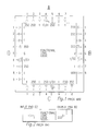
- FIG. 1 illustrates a schematic of a die 1 containing functional core logic (FCL) 2, and input and output buffering to pad locations.
- FCL functional core logic
- the variety of pad buffering shown includes: inputs (I), 2-state outputs (2SO), 3-state outputs (3SO) , open drain outputs (ODO), input and 3SO bidirectionals (I/O1), and input and ODO bidirectionals (I/O2).
- the FCL 2 could be a custom or semicustom (ASIC) implementation comprising: microprocessors, combinational logic, sequential logic, analog, mixed signal, programmable logic, RAMs, ROMs, Caches, Arrays, DSPs, or combinations of these and/or other functions.
- the die 1 is shown having a top side A, right side B, bottom side C, and left side D for convenience of description in regard to its position on the wafer.
- the die 1 also has at least one voltage supply (V) pad and at least one ground (G) pad for supplying power to the die 1.
- Side A has pad locations 1-7
- B has pad locations 1-8
- C has pad locations 1-8
- D has pad locations 1-9.
- the arrangement of the buffer/pad combinations on each side (A,B,C,D) corresponds to the desired pinout of the package that the die 1 will be assembled into, or to signal terminals on a multi-chip module (MCM) substrate onto which the die 1 will be connected.
- Figure 2 is a cutaway side view of the die showing an input pad at D2 and an output pad at B2 both connected to the FCL 2.
- Figure 3A shows an example wafer containing 64 of the die of Figure 1.
- Figure 3B shows the position of each die 1 on the wafer with respect to sides A, B, C, and D.
- the phantom die 1 1 in dotted line shows how the wafer would be packed to yield more die per wafer. Notice that even when the die 1 is tightly packed on the wafer (i.e. the phantom die 1 1 locations utilized), there is still area at the periphery of the wafer where die cannot be placed. This is due to the circular shape of the wafer versus the square/rectangular shape of the die.
- This unusable peripheral area 3 of the wafer can be used to place test points (pads), test circuitry, and conductors for routing test signals and power and ground to die.
- Figure 4 shows how conventional die testing is performed using a tester and pad probe assembly.
- the probe assembly is positioned over a selected die 1 and lowered to make contact with the die pads. Once contact is made the tester applies power and checks for high current. If current is high a short exists on the die and test is aborted and the die is marked (usually by an ink color) as bad. If current is normal, then testing proceeds by applying test patterns to the die and receiving test response from the die. If the test fails the die 1 is marked as bad. If the test passes the die is good and not marked, or if marked, marked with a different ink color. During testing the die current can be monitored to see if it stays within a specified range during the test. An out of range current may be marked as a high current functional failure.
- the present invention provides: a die framework comprising die resident circuitry and connections to selectively provide either a bypass mode wherein the die has direct pad-to-pad connectivity or a functional mode wherein the die has die pad to functional core logic connectivity; a fault tolerant circuit and method to select a die on a wafer to be placed in functional mode while other die remain in bypass mode; a method and apparatus for (1) electronically selecting one die on a wafer to be placed in functional mode for testing while other die on the wafer are in bypass mode, (2) testing that selected die, and (3) repeating the electronic selection and testing steps on other die; and a method and apparatus for (1) electronically selecting a plurality of diagonally positioned die on the wafer to be placed in functional mode for testing while other die on the wafer are in bypass mode, (2) testing the selected group of diagonally positioned die in parallel, and (3) repeating the electronic selection and testing steps on other groups of diagonally positioned die.
- the present invention provides improved testing of unsingulated die on wafer.
- the invention provides the following exemplary improvements: (1) electronic selection and testing of unsingulated die on wafer, (2) faster testing of dies on wafer, (3) elimination of expensive, finely designed mechanical wafer probes, (4) the ability to at-speed test unsingulated die on wafer, (5) the ability to test a plurality of unsingulated die in parallel, and (6) the ability to simplify the burn-in testing of unsingulated die.
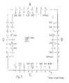
- Figure 5 a die 1 schematic similar to that of Figure 1 is shown. Like Figure 1, the die has sides A, B, C, and D and corresponding pad sites for input, output, input/output, V and G.
- Figure 5 includes additional pad sites A8 and B9 referred to as bypass, and an additional pad site C9 referred to as mode.
- the mode pad is buffered like a data input.
- mode is at a predetermined logic level, say high, the die schematic appears as shown in Figure 5, and the die is in its functional mode which is exactly the equivalent of the die in Figure 1.
- the FCL 2 input, output, and input/output pads are enabled and the die performs its intended function.
- the bypass pads are not used.
- the die 1 of Figure 5 is schematically shown as it would operate in the bypass mode of the present invention.
- the die is placed in bypass mode by taking the mode pad to a logic state opposite that of the functional mode logic state, in this case a logic low.
- bypass mode the die's FCL 2, input, output, and input/output buffers are disabled and pad sites of corresponding position between sides A and C and between sides D and B are electrically connected.
- bypass mode the die 1 is transformed into a simple interconnect structure between sides A and C and between sides D and B.
- the interconnect structure includes a plurality of conductors extending parallel to one another between sides A and C, and a further plurality of conductors extending parallel to one another between sides D and B. While in bypass mode, signals from a tester apparatus can flow through the interconnects between A and C and between D and B to access and test a selected die 1 on a wafer.
- bypass pads of Figure 5 provide pad-to-pad connectivity when the number of pads on opposite sides are not equal.
- bypass pads A8 and B9 provide connecting pads for functional pads C8 and D9 respectively.
- the bypass connections between opposite side die pads form a low impedance, bidirectional signaling path through the die from pad to pad.
- the bypass connections between two sides are preferably designed to have an equal propagation delay between opposite side pads to avoid skewing of test signals passed through bypassed die.
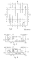
- the sides of a die selected for testing need to be driven by signals from the adjacent sides of top, right, bottom, and left neighboring die which are in bypass mode ( Figure 6).
- the neighboring die In order for the neighboring die to be tested, it is placed in functional mode, and: (1) all signals required at its A side are provided at the C side of the top neighboring bypassed die, (2) all signals required at its B side are provided at the D side of the right neighboring bypassed die, (3) all signals required at its C side are provided at the A side of the bottom neighboring bypassed die, and (4) all signals required at its D side are provided at the B side of the left neighboring bypassed die.
- Figures 7 through 14 depict cross section views of example circuitry and connections which can achieve the framework for selective die functional and bypass modes.
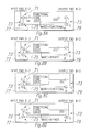
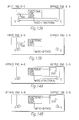
- Exemplary Figures 7A and 7B illustrate side views of the D1 input pad and the B1 3-state output pad of the die 1 in Figures 5 and 6.
- a switch 71 is provided between the input pad and input buffer to allow isolating the input pad from the input buffer during bypass mode, and an input state holder (ISH) circuit is provided between the switch and input buffer to allow holding a predetermined input state to the input buffer (which drives the FCL 2) while the switch is open during bypass mode.
- Gating circuitry such as an AND gate (A), is provided in the control path between the FCL 2 and 3-state output buffer to allow the 3-state output buffer to be disabled during bypass mode.
- a selectable connection path 73 between the input and output pad includes a conductor 75 connected between a switch 77 associated with the input pad and a switch 79 associated with the output pad, which switches are operable to connect conductor 75 to G or to the input and output pads.
- the mode pad is connected to the switches, ISH and gate A as shown such that when the mode pad is in one logic state the die 1 is in functional mode and when in the opposite logic state the die is in bypass mode.
- the mode pad can be connected to FCL 2 as shown to permit disabling of clocks or other operations in FCL during bypass mode.
- ISH can be realized with a 3-state data buffer having a data input connected to a desired logic level (logic "1" in this example) and a data output connected to the input of the input buffer and a 3-state control input connected to the mode pad.
- the desired logic level for a given FCL input could be, for example, a logic level which minimizes current flow in the FCL 2 during bypass mode.
- the 3-state buffer is enabled during bypass mode and 3-stated during functional mode. If the desired logic level is a don't care condition, then the bus holder BH of exemplary Figure 12B can be used to hold the last input logic level during bypass mode.
- switches 77 and 79 When in functional mode (Figure7A), the switches 77 and 79 connect the conductor 75 to G which provides a ground plane on the conductor and prevents AC coupling between the input and output pads.
- switches 77 and 79 and the conductor 75 When in bypass mode ( Figure 7B), the switches 77 and 79 and the conductor 75 provide a low impedance, bidirectional signaling path connection between the input and output pads.
- switch 71 is open to isolate FCL 2 from the input pad, and the 3-state output buffer is disabled (3-stated) via AND gate A to isolate FCL 2 from the output pad.
- Figures 8-11 show the use of the bypass circuitry with other types of pad buffers.
- Figures 13 and 14 show the use of the bypass circuitry between functional input (D9) and bypass (B9) pads, and functional output (C8) and bypass (A8) pads.
- a further switch 81 is used to isolate the 2-state output buffer from output pad B2 during bypass mode.
- Figures 8C and 8D are similar to Figures 8A and 8B except a 3-state output buffer is used instead of a 2-state output buffer and switch 81, in order to eliminate the impedance of switch 81 during functional mode.
- Figures 11A and 11B illustrate I/O pads with 3-state (I/O1) and open drain (I/O2) outputs.
- the input buffers and the 3-state output buffer of Figures 11A and 11B are arranged as described above with respect to Figures 7A and 7B.
- the open drain output buffer of Figures 11A and 11B has its input connected to an output of an OR gate (O) which has one input driven by FCL 2 and another input driven by the logical inverse of the mode signal, whereby the open drain output will float high during bypass mode assuming that the mode signal selects bypass mode when low.
- OR gate OR gate
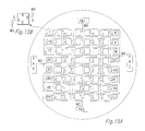
- FIG 15A illustrates an example of how wafer voltage (WV) and wafer ground (WG) bussing can be distributed to the V and G pads of each die 1 on the wafer.
- the WV bussing is shown originating from areas of the wafer designated as probe area PA1 and probe area PA2.
- the WG bussing is shown originating from probe area PA3 and probe area PA4.
- Probe areas PA1-4 are positioned at the periphery of the wafer and in areas where die 1 cannot be placed, as mentioned in regard to Figure 3A.
- Figure 15B illustrates how WV and WG are coupled to the V and G die pads (see Figures 1 and 5) through diodes. By placing diodes between WG and G and WV and V, conventional localized probing and power up of an individual die 1 can occur without powering up neighboring dies.
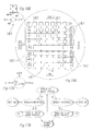
- Figure 16A illustrates an exemplary scheme for performing fault tolerant selection of unsingulated die 1 on a wafer.
- the scheme involves the placement of a small circuit, referred to as a die selector 161, in the scribe lane adjacent each die on the wafer.
- the die selector 161 shown in Figure 16B includes an I/O terminal S1, an I/O terminal S2, a mode output terminal, and connections to WV and WG for power.
- the die selector's mode output is connected to the mode pad of an associated die.
- the die selectors are connected in series via their S1 and S2 terminals.
- S1 of the first die selector in the series (at die 1) is connected to PA4, and S2 of the last die selector in the series (at die 64) is connected to PA3.
- the die selector is placed in the scribe lane instead of on the die 1, the mode pad of the die can be physically probed if required, to override the die selector mode output.
- This feature permits any die 1 to be tested using the conventional probe testing technique.
- the mode output of the die selector drives only the mode pad of a single die, it can be designed with a relatively weak output drive so that the conventional probe tester can easily override the mode output without any damage to the mode output.
- Power is applied to WV and WG by probing PA1-PA4.
- all the die selectors get reset to a state that forces their mode outputs low, which causes all die to be placed in bypass mode. If excess current is detected at power up (indicating perhaps a short between WV and WG), the wafer can be powered down and tested using the traditional mechanical probing technique (note that the diodes of Figure 15B allow for this). If normal current is detected (meaning that all die have successfully powered up in bypass mode) further testing according to the present invention may be performed.
- testing of the die selectors can occur by injecting clock pulses from PA4 to S1 of the upper left die selector (adjacent die 1) and monitoring S2 of the lower left die selector (adjacent die 64) at PA3. If the serial path between the die selectors is intact, a clock pulse output will occur on lower left S2 after 65 clock pulses have been applied to upper left S1. On the falling edge of the first injected clock pulse, die 1 is switched from bypass mode to functional mode by the mode output of the associated die selector going high. All other die are forced to remain in bypass mode by their die selectors' mode outputs being low.
- the upper left die selector connects its S1 and S2 terminals so that subsequent S1 clocks are output on S2.
- die 1 is placed back into bypass mode by its die selector's mode output going low.
- This second clock pulse is transferred through the upper left die selector to the next die selector via the S1 to S2 connection.
- the die 2 selector connects its S1 and S2 terminals and switches die 2 from bypass to functional mode by driving the mode output high. This process continues on to die 64 and its die selector.
- die 64 On the rising edge of the 65th injected clock pulse, die 64 is placed back into the bypass mode by its die selector's mode output going low, and the 65th clock pulse is output from S2 to PA3.
- the current flow to and/or from the wafer via WV and WG can be monitored during each rising and falling clock edge to see if the expected current increase and decrease occurs as each die 1 transfers in sequence between bypass and functional modes.
- the wafer current fluctuations By sensing the wafer current fluctuations, it is possible to detect when a die that should be selected (i.e. in functional mode) is not selected, which could indicate a defect in the die selector arrangement as discussed further below.
- the above description illustrates how to test and operate the die selector path from PA4 to PA3.
- the same test and operation mode is possible by clocking S2 of the lower left die selector from PA3 and monitoring S1 of the upper left die selector at PA4.
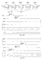
- the die selector model of exemplary Figure 17A and state diagram of exemplary Figure 17B illustrate die selector operation modes in detail. From Figure 17B it is seen that the die selector responds to a first received S1 or S2 clock pulse to output mode control (on the falling edge) to place the connected die in functional mode so that it can be tested.
- a rising edge on the same signal (say S1) causes the tested die to be placed back into bypass mode and also drives the S1 input of the next die selector. On the next successive falling edge the die associated with the next die selector is switched into functional mode for testing. And so on.
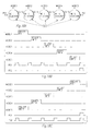
- FIGS 18A-18C illustrate in detail the die selector operation described above.
- PS1 and PS2 in Figure 18 are externally accessible terminals (like PA3 and PA4) for injecting and receiving clock pulses.
- the die selectors operate bidirectionally as mentioned above. The reason for the bidirectional operation is for fault tolerance, (i.e. a broken connection between two die selectors can be tolerated).
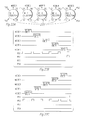
- An example of the fault tolerant operation of the die selector is shown in Figures 19A-19C.
- Figure 19A an open circuit fault exists between the 2nd and 3rd die selectors.
- PS1 clock activations can only select die 1 and 2 ( Figure 19B).
- PS2 clock activations can select die 5, 4, and 3 ( Figure 19C).
- the die selector arrangement is able to select and place a given die in functional mode for testing.
- Wafers such as shown in Figure 16A may also be connected in series via the S1/S2 signals to allow selection of die on many wafers as shown in Figure 19D.
- S2 of the lower left die of wafer 191 is connected, via PA3 of wafer 191 and external conductor 193 and PA4 of wafer 195, to S1 of the upper left die of wafer 195.
- An analogous connection also exists between wafers 195 and 197.
- External probe connections at PA4 of wafer 191 and PA3 of wafer 197 permit the die selection scheme described above with respect to Figures 16A-18C to be applied to die on plural wafers.
- Exemplary Figures 20 and 21 illustrate how to further improve die selector fault tolerance by the addition of a second pair of I/O terminals S3 and S4 in die selector 201.
- the S3 and S4 serial connection path is shown routed between PA1 and PA2 in the vertical scribe lanes. Separating the S1/S2 (horizontal scribe lanes) and S3/S4 (vertical scribe lanes) routing is not required, and both routings could be in the same horizontal or vertical lanes if desired. It is clear in the example of Figure 20A that routing S1 and S2 in the horizontal lanes and routing S3 and S4 in the vertical lanes will result in different die selection orders, i.e. S1 and S2 select die order 1, 2, 3 ... 64 or die order 64, 63, 62 ... 1, whereas S3 and S4 select die order 1, 16, 17, ... 64 ... 8 or die order 8, 9, 24 ... 1.
- Exemplary Figures 21A and 21B illustrate the model and state diagram of the improved fault tolerant die selector 201 of Figures 20A and 20B.
- the operation of the die selector 201 of Figure 21A is similar to that of the die selector 161 of Figure 17A except that the die selector 201 has redundant bidirectional selection paths. Redundant selection paths allow the die selector 201 to maintain operation even when one of its selection paths is rendered inoperable by gross defects that defeat the fault tolerance features provided in the single path die selector 161 of Figure 17A.
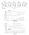
- FIGs 22A-24C operational examples using dual selection path die selectors 201 are shown. For clarity, the examples show both paths (S1 and S2, and S3 and S4) routed together (in same scribe lanes) to the same sequence of die 1 through 5. This differs from the example routing of Figure 20A where S1 and S2 are routed in horizontal lanes and S3 and S4 are routed in vertical lanes, and thus each path has a different sequence of die selection.
- Figure 22B shows PS1 selecting die in the order 1, 2, 3, 4 & 5.
- Figure 22C shows PS2 selecting die in the order 5, 4, 3, 2 & 1.
- Figure 23A shows PS3 of Figure 22A redundantly selecting die in the same order as PS1 (Figure 22B).
- Figure 23B shows PS4 of Figure 22A redundantly selecting die in the same order as PS2 ( Figure 22C). Both paths can tolerate a single defect (open circuit) as shown in Figures 19A-19C.
- Figure 24A shows a multiple defect example (two open circuits) on the S1 and S2 path that would disable access to intermediate die 2, 3 & 4 if only the S1 and S2 path were provided.
- Figures 24B-24C illustrate that PS1 can only select die 1, and PS2 can only select die 5 with the defects shown in Figure 24A.
- the S3 and S4 path can be used to select die 2, 3 & 4 as illustrated in Figures 23A-23B.
- die selector 201 is that it can maintain access to die even if one of the paths is critically disabled by multiple defects.
- Figures 24F and 24G illustrate an exemplary implementation of the die selector 161 defined in Figures 17A-18C.
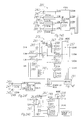
- input terminals S1 and S2 are respectively connected to inputs S1IN and S2IN of a die selector state machine 241 via respective input data buffers 243 and 245.
- the die selector state machine 241 outputs the mode signal and enable signals S1ENA and S2ENA.
- Enable signals S1ENA and S2ENA respectively control output data buffers 247 and 249.
- the output of input data buffer 243 is connected to the input of output data buffer 249 to permit signals received at terminal S1 to be output on terminal S2 when enable signal S2ENA enables output data buffer 249.
- the output of input data buffer 245 is connected to the input of output data buffer 247 to permit signals received at terminal S2 to be output on terminal S1 when enable signal S1ENA enables output data buffer.247.
- Exemplary Figure 24G illustrates the die selector state machine 241 of Figure 24F in greater detail.
- a conventional power-up reset circuit initially clears D flip-flops 251, 253 and 255 when the die selector is initially powered up.
- the pass signal output from flip-flop 255 is inverted at one input of AND gate 259.
- the other input of AND gate 259 which is driven by the output of OR gate 257, is thus qualified at gate 259 by the pass signal upon initial power up. Because flip-flop outputs QS1 and QS2 are low after initial power-up, the mode signal is therefore low after power-up.
- the output of AND gate 261 is connected to the D input of flip-flop 253 via delay element 267, and the output of AND gate 263 is connected to the D input of flip-flop 251 via delay element 269.
- Delay elements 267 and 269 are designed to have a propagation delay which is greater than the propagation delay of OR gate 271.
- a rising edge of a first clock pulse on S1IN causes a logic zero to be clocked through flip-flop 255, thereby maintaining the pass signal at its initial low state.
- the D input of flip-flop 251 will still be high due to the delay element 269, thus causing flip-flop output QS1 to go high.
- the mode signal is driven high via OR gate 257 and AND gate 259.
- the output data buffer 249 of Figure 24F is enabled via signal S2ENA, the input S2IN is disqualified at AND gate 261, and the D input of flip-flop 255 is driven high via OR gate 265.
- the rising edge of the second clock pulse on terminal S1 of Figure 24F passes directly to terminal S2 via output data buffer 249, and also passes through AND gate 263 and OR gate 271 of Figure 24G to clock flip-flop 255 and take the pass output thereof high, thereby driving the mode signal low.
- the next falling edge on terminal S1 will pass through data output buffer 249 to terminal S2, and will maintain the QS1 output of flip-flop 251 in the high logic state.
- the positive edge of the third clock pulse received on terminal S1 will pass through data output buffer 249 to terminal S2, and will also clock a logic one through flip-flop 255 so that the pass signal will maintain the mode output low via AND gate 259.
- the negative edge of the third clock pulse will maintain the logic one at the QS1 output of flip-flop 255.
- die selector 161 The bidirectional feature of die selector 161 should be apparent from Figures 24F and 24G. That is, if a succession of clock pulses had occurred on terminal S2 rather than on terminal S1, then output QS2 of flip-flop 253 would have been driven high to enable data output buffer 247 and disable the S1IN signal via AND gate 263.
- the mode signal behaves exactly the same in response to a succession of clock pulses on terminal S2 as described above with respect to the succession of clock pulses on terminal S1, and the terminal S1 will receive the second and all successive clock pulses input on terminal S2.
- Exemplary Figures 24D and 24E show an implementation of die selector 201 which is similar to the implementation of die selector 161 illustrated in Figures 24F and 24G.
- the output of data input buffer 243 is connected to the input of data output buffer 249 as in Figure 24F
- the output of data input buffer 245 is connected to the input of data output buffer 247 as in Figure 24F.
- the output of data input buffer 275 is connected to the input of data output buffer 277
- the output of data input buffer 281 is connected to the input of data output buffer 279.
- the die selector state machine 273 of Figure 24D is shown in greater detail in Figure 24E.
- the die selector state machine 273 of Figure 24D represents an extension of the die selector state machine of 241 of Figure 24G.
- An additional AND gate 287, delay element 293, and flip-flop 283 have been added for terminal S3, and an additional AND gate 289, delay element 291 and flip-flop 285 have been added for terminal S4.
- the operation of these additional elements is identical to the operation described above with respect to the corresponding elements in Figure 24G.
- a first falling clock pulse edge on terminal S3 will result in the QS3 output of flip-flop 283 going high to drive the mode signal high and to enable the data output buffer 277 to connect terminal S3 to terminal S4.
- the rising edge of the second clock pulse on terminal S3 will clock a logic one through flip-flop 255 so that the pass signal will drive the mode signal low again via AND gate 259.
- the falling edge of a first clock pulse on terminal S4 will drive high the QS4 output of flip-flop 285, which drives the mode signal high and enables data output buffer 279 to connect terminal S4 to terminal S3.
- the decoder circuit 291 receives QS1-QS4 as inputs and provides DS1-DS4 as outputs.
- the decoder circuit 291 drives DS2-DS4 active high, which disables signals S2IN, S3IN and S4IN at AND gates 261, 287 and 289.
- the decoder circuit drives signals DS1, DS3 and DS4 active high
- the decoder circuit drives signals DS1, DS2 and DS4 active high
- the decoder circuit drives signals DS1-DS3 active high.
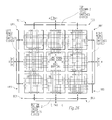
- probe test pads in PA1 are bussed (via A-Bus) to one side of eight top column switch groups (TC1-8), representative switch group TC8 being shown in Figure 25D.
- Each top column switch group also receives a select top column signal (such as STC8) from PA1 that opens or closes the switches.
- the other side of each top column switch group is bussed to the A side (recall Figure 5) pads of die 1, 2, 3, 4, 5, 6, 7, and 8.
- probe test pads in PA2 are bussed (via B-Bus) to one side of eight right row switch groups (RR1-8), representative switch group RR8 being shown in Figure 25C.
- Each right row switch group also receives a select right row signal (such as SRR8) from PA2 that opens or closes the switches.
- the other side of each right row switch group is bussed to the B side pads of die 8, 9, 24, 25, 40, 41, 56, and 57.
- probe test pads in PA3 are bussed (via C-Bus) to one side of eight bottom column switch groups (BC1-8), representative switch group BC1 being shown in Figure 25E.
- Each bottom column switch group also receives a select bottom column signal (such as SBC1) from PA3 that opens or closes the switches.
- the other side of each bottom column switch group is bussed to the C side pads of die 57, 58, 59, 60, 61, 62, 63, and 64.
- probe test pads in PA4 are bussed (via D-Bus) to one side of eight left row switch groups (LR1-8), representative switch group LR1 being shown in Figure 25B.
- Each left row switch group also receives a select left row signal (such as SLR1) from PA4 that opens or closes the switches.
- SLR1 select left row signal
- the other side of each left row switch group is bussed to the D side pads of die 1, 16, 17, 32, 33, 48, 49, and 64.
- PA1-4, the switch groups, and bussing to connect them can all be located in the unusable peripheral area (recall Figure 3A) of the wafer.
- each die on the wafer excluding the boundary die, such as die 1, 2, 3, 16, 17 etc. is connected at its top (A), right (B), bottom (C) and left (D) side pad sites to neighboring die pad sites by way of short busses that bridge across the scribe lanes between the die. Due to the regularity of the die and their positioning on the wafer, vertical pad bussing is provided between each neighboring die on sides A and C, and horizontal pad bussing is provided between each neighboring die on sides B and D.
- the pads of boundary die are similarly bussed to neighboring die pads, but only on at most three sides, since at least one of the boundary die sides will always be connected to a switch group.
- the wafer also comprises: (1) die having selectable functional and bypass modes as described in Figures 5-14, (2) WV and WG bussing as shown in Figures 15A-15B, and (3) fault tolerant die selectors as described in Figures 16 - 24.
- Each switch group when selected (switches closed), provides a low impedance, bidirectional signaling path.
- the bussing connections between PA1-4 and the switch groups (TC1-8, LR1-8, BC1-8, RR1-8), between the switch groups and the die sides (A, B, C, D), and between the die sides, provide a low impedance, bidirectional signaling path.
- the die's internal bypass pad-to-pad connections also provide low impedance, bidirectional signaling paths.
- a probe When testing is to be performed, a probe is positioned onto the wafer at the pad areas PAT1-4.
- PA1-4 are large compared to the pad area of each die, and therefore the mechanical requirements of the probe design are simpler and less costly than conventional probes which are elegantly designed for contacting tiny die pads.
- the probe since the present invention allows for a die to be electronically selected for testing, the probe needs to be positioned onto the wafer only once, which reduces test time when compared to conventional multiple probing of a wafer. This test time reduction can significantly decrease the cost of wafer testing, which in turn decreases the cost of the die and packaged IC.
- the probe does not contact any die pads, no damage to die pads occurs during the wafer probe and die test procedure.
- the relatively large probe target area provided by PA1-4 lends itself well to computer controlled and automated test probing processes.
- the tester After the probe contacts the wafer at PA1-4, power is applied to the wafer to power up the die and die selectors.
- the tester can quickly detect a high current situation and remove power from the wafer as necessary. Wafer processing faults could cause shorts between WG and WV bussing or a die or die selector could have a V and G short. If the wafer fails the high current test at power up, die testing can still be done by conventional die probing techniques.
- the die selectors can be tested as previously described with regard to Figures 16-24. If the die selectors fail in all fault tolerant modes, the wafer can still be tested conventionally. If the die selectors pass, the row and column bussing paths can be tested. To test row 1 and column 1 ( Figures 25 and 26), the LR1, RR1, TC1 and BC1 switch groups are closed and, with all die in bypass mode, an external tester (such as in Figure 4) passes signals between PA4 and PA2 to test row 1 bussing and between PA1 and PA3 to test column 1 bussing.
- an external tester such as in Figure 4
- This step tests, (1) the PA1-4 to switch group bussing, (2) the switch group closures, (3) the switch group to boundary die bussing, (4) the die bypass mode, and (5) the die-to-die pad bussing. This step is repeated on all rows and columns. If a row or column fails, die associated with that row and column can be tested conventionally. After testing row and column connectivity, the die can be tested.
- the die test starts by outputting a first pulse to S1 (could be S2, or S3 or S4 if die selector 201 is used) from PA4 to cause the upper left die selector to switch die 1 from bypass to functional mode, and then closing switch groups LR1, TC1, RR1 and BC1, and then testing die 1 using the external tester which is connected to die 1 via PA1-4, the closed switch groups and the row 1 and column 1 bussing paths.
- S1 could be S2, or S3 or S4 if die selector 201 is used
- S1 could be S2, or S3 or S4 if die selector 201 is used
- This test sequence is repeated on all die on the wafer.
- Figure 26 illustrates in detail the testing of die 15 via the row 2 and column 2 bussing paths. Different types of testing can be performed on a selected die.
- a first test is a DC test where the objective is to verify the I/O parametrics and the logical correctness of the die.
- a second test is a functional test wherein the die is functionally tested at its intended operating speed.
- Some high reliability applications require an environmental (or burn in) test where the die is tested in chambers where temperature, humidity, and vibration can be cycled during testing.
- Die that pass DC testing may fail functional and environmental testing, so at wafer level it is important to test die in DC, functional, and perhaps environmental test mode to prevent bad die from being packaged into IC form or assembled on MCMs.
- the D and A sides of die 15 receive test signaling from PA4 and PA1 through only bypassed die 16 and 2 respectively, whereas test signaling at sides B and C of die 15 must traverse more than one bypassed die (see Figure 25A) before arriving from PA2 and PA3, respectively.
- the die bypass signaling delay and die-to-die bussing delays can easily be modeled in tester software so that the tester can compensate for the delays through row and column bussing paths that traverse different numbers of die in bypass mode. In this way, test signaling between the tester and target die under test will occur correctly, independent of the number of bypassed die that exists in the row and column bussing paths connected to the A, B, C, and D sides of the die under test.
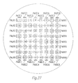
- a wafer bussing structure where each row and column has its own pair of probe areas.
- probe area left row 1 (PALR1) and probe area right row 1 (PARR1) serve as the row 1 probe areas
- probe area top column 1 (PATC1) and probe area bottom column 1 (PABC1) serve as the column 1 probe areas.
- PATC1 and PABC1 serve as the column 1 probe areas.
- the die-to-die bussing is the same as described previously relative to Figures 25-26.
- the probe areas can exist in the unused peripheral area of the wafer.
- the probe areas could be eliminated altogether and the pad sites at the A, B, C and D sides of the top, right, bottom, and left boundary die could be probed if desired.
- Figure 28 illustrates an example of how each row can be supplied, via its left and right probe areas PALRn and PARRn, with a unique V and G connection.
- Figure 29 illustrates how each row can be supplied, via its left and right probe areas PALRn and PARRn, with a unique die selector signaling connection.
- the power and die selector connections could also be arranged column-wise so that PATCn and PABCn would provide each column with unique power supply and die selection.
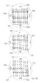
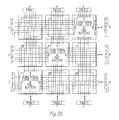
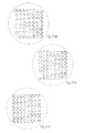
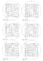
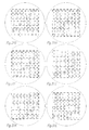
- Exemplary Figure 30 illustrates in detail how diagonally positioned die 17, 15, and 3 are tested in parallel. If a group of diagonally positioned die are placed in functional mode (via each row's independently operated die selectors of Figure 29) while all other die are in bypass mode, then further test time reduction can be achieved by parallel (i.e. simultaneous) testing of the group of diagonally positioned die via the dedicated row and column bussing paths and probe areas shown in Figure 30.
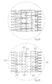
- Figures 31A through 310 illustrate the parallel die testing approach as it proceeds across all groups of diagonally positioned die on the wafer. These steps of parallel die testing are listed below, using the die numbering of Figure 27.
- the above-described parallel testing of die on wafer can reduce wafer test time as compared to individual, sequential testing of die on wafer.
- the present invention is also applicable to IDDQ testing of each die on the wafer.
- IDDQ testing is the monitoring of current to an IC/die during the application of test patterns. A higher than expected current at a particular test pattern may indicate a defect.
- the WV and WG bussing arrangement of Figure 15A is adequate when performing IDDQ testing in the one-die-at-a-time arrangement of Figures 25-26, because any unexpected current on WV and/or WG can be attributed to the one die that is in functional mode.
- row-specific V and G bussing of the type shown in Figure 28 permits unexpected V and G current to be attributed to the correct die of the diagonal grouping being tested.
- the WV and WG bussing of the type shown in Figure 15A can be used in Figures 30-31.
- an additional probe access area could be provided for power supply bussing, in which case PALRn and PARRn need not provide power.
- the present invention permits the tester probe design to be greatly simplified relative to prior art designs, resulting in less expensive testers.
- the vendor can afford to maintain their own wafer tester.
- This permits the vendor to sell complete wafers (rather than singulated die) to customers, who can then repeat the vendor's wafer test and verify the results, and then advantageously singulate the die for themselves.
- the vendor is thus relieved of the risk of damaging die during singulation, while the customers can advantageously obtain unpackaged die (on wafer), verify that the die have not been damaged in transit from the vendor, and then singulate the die themselves.
Landscapes
- Engineering & Computer Science (AREA)
- General Engineering & Computer Science (AREA)
- Physics & Mathematics (AREA)
- General Physics & Mathematics (AREA)
- Semiconductor Integrated Circuits (AREA)
- Testing Or Measuring Of Semiconductors Or The Like (AREA)
- Tests Of Electronic Circuits (AREA)
Applications Claiming Priority (8)
| Application Number | Priority Date | Filing Date | Title |
|---|---|---|---|
| US818495P | 1995-10-31 | 1995-10-31 | |
| US818695P | 1995-10-31 | 1995-10-31 | |
| US813895P | 1995-10-31 | 1995-10-31 | |
| US710295P | 1995-10-31 | 1995-10-31 | |
| US8138 | 1995-10-31 | ||
| US8184 | 1995-10-31 | ||
| US7102 | 1995-10-31 | ||
| US8186 | 1995-10-31 |
Publications (3)
| Publication Number | Publication Date |
|---|---|
| EP0786667A2 true EP0786667A2 (de) | 1997-07-30 |
| EP0786667A3 EP0786667A3 (de) | 1999-07-07 |
| EP0786667B1 EP0786667B1 (de) | 2004-10-27 |
Family
ID=27485659
Family Applications (1)
| Application Number | Title | Priority Date | Filing Date |
|---|---|---|---|
| EP96307905A Expired - Lifetime EP0786667B1 (de) | 1995-10-31 | 1996-10-31 | Verfahren und Vorrichtung zur Prüfung von integrierten Schaltungen |
Country Status (5)
| Country | Link |
|---|---|
| EP (1) | EP0786667B1 (de) |
| JP (1) | JP4041550B2 (de) |
| KR (1) | KR100402868B1 (de) |
| DE (1) | DE69633713T2 (de) |
| TW (1) | TW454291B (de) |
Cited By (8)
| Publication number | Priority date | Publication date | Assignee | Title |
|---|---|---|---|---|
| WO2006061011A1 (de) * | 2004-12-10 | 2006-06-15 | X-Fab Semiconductor Foundries Ag | Test von eingebetteten schaltungen mit hilfe von testinseln |
| EP1691297A3 (de) * | 2005-02-12 | 2006-09-06 | Broadcom Corporation | Verfahren und System für Eingangs/Ausgangskontakte in einem mobilen Multimediaprozessor |
| US7872487B2 (en) | 2007-12-27 | 2011-01-18 | Robert Bosch Gmbh | Semiconductor wafer having a multitude of sensor elements and method for measuring sensor elements on a semiconductor wafer |
| CN102684681A (zh) * | 2011-03-11 | 2012-09-19 | 阿尔特拉公司 | 包括i/o堆叠的系统以及用于制造此类系统的方法 |
| US8716814B2 (en) | 2004-07-14 | 2014-05-06 | Semiconductor Energy Laboratory Co., Ltd. | Wireless processor, wireless memory, information system, and semiconductor device |
| US9823290B2 (en) | 2013-03-05 | 2017-11-21 | Infineon Technologies Ag | Method for testing components and measuring arrangement |
| US9929220B2 (en) | 2009-01-08 | 2018-03-27 | Semiconductor Energy Laboratory Co., Ltd. | Light emitting device and electronic device |
| US12380815B2 (en) | 2014-10-28 | 2025-08-05 | Semiconductor Energy Laboratory Co., Ltd. | Light-emitting device with circular polarizing plate over bonding layer |
Families Citing this family (2)
| Publication number | Priority date | Publication date | Assignee | Title |
|---|---|---|---|---|
| JP4572564B2 (ja) * | 2004-04-05 | 2010-11-04 | パナソニック株式会社 | 半導体装置 |
| JP2013050860A (ja) * | 2011-08-31 | 2013-03-14 | Renesas Electronics Corp | マイクロコンピュータ及びマルチマイクロコンピュータシステム |
Family Cites Families (3)
| Publication number | Priority date | Publication date | Assignee | Title |
|---|---|---|---|---|
| US4092733A (en) * | 1976-05-07 | 1978-05-30 | Mcdonnell Douglas Corporation | Electrically alterable interconnection |
| US4286173A (en) * | 1978-03-27 | 1981-08-25 | Hitachi, Ltd. | Logical circuit having bypass circuit |
| JPS62220879A (ja) * | 1986-03-22 | 1987-09-29 | Hitachi Ltd | 半導体装置 |
-
1996
- 1996-10-31 KR KR1019960050583A patent/KR100402868B1/ko not_active Expired - Lifetime
- 1996-10-31 EP EP96307905A patent/EP0786667B1/de not_active Expired - Lifetime
- 1996-10-31 DE DE69633713T patent/DE69633713T2/de not_active Expired - Lifetime
- 1996-10-31 JP JP29082796A patent/JP4041550B2/ja not_active Expired - Lifetime
- 1996-11-25 TW TW085114484A patent/TW454291B/zh not_active IP Right Cessation
Non-Patent Citations (1)
| Title |
|---|
| None |
Cited By (13)
| Publication number | Priority date | Publication date | Assignee | Title |
|---|---|---|---|---|
| US8716814B2 (en) | 2004-07-14 | 2014-05-06 | Semiconductor Energy Laboratory Co., Ltd. | Wireless processor, wireless memory, information system, and semiconductor device |
| US9425215B2 (en) | 2004-07-14 | 2016-08-23 | Semiconductor Energy Laboratory Co., Ltd. | Wireless processor, wireless memory, information system, and semiconductor device |
| US9087280B2 (en) | 2004-07-14 | 2015-07-21 | Semiconductor Energy Laboratory Co., Ltd. | Wireless processor, wireless memory, information system, and semiconductor device |
| US7994806B2 (en) | 2004-12-10 | 2011-08-09 | X-Fab Semiconductor Foundries Ag | System and method for testing embedded circuits with test islands |
| WO2006061011A1 (de) * | 2004-12-10 | 2006-06-15 | X-Fab Semiconductor Foundries Ag | Test von eingebetteten schaltungen mit hilfe von testinseln |
| EP1691297A3 (de) * | 2005-02-12 | 2006-09-06 | Broadcom Corporation | Verfahren und System für Eingangs/Ausgangskontakte in einem mobilen Multimediaprozessor |
| US7872487B2 (en) | 2007-12-27 | 2011-01-18 | Robert Bosch Gmbh | Semiconductor wafer having a multitude of sensor elements and method for measuring sensor elements on a semiconductor wafer |
| US9929220B2 (en) | 2009-01-08 | 2018-03-27 | Semiconductor Energy Laboratory Co., Ltd. | Light emitting device and electronic device |
| US10361258B2 (en) | 2009-01-08 | 2019-07-23 | Semiconductor Energy Laboratory Co., Ltd. | Light emitting device and electronic device |
| CN102684681A (zh) * | 2011-03-11 | 2012-09-19 | 阿尔特拉公司 | 包括i/o堆叠的系统以及用于制造此类系统的方法 |
| CN102684681B (zh) * | 2011-03-11 | 2016-08-03 | 阿尔特拉公司 | 包括i/o堆叠的系统以及用于制造此类系统的方法 |
| US9823290B2 (en) | 2013-03-05 | 2017-11-21 | Infineon Technologies Ag | Method for testing components and measuring arrangement |
| US12380815B2 (en) | 2014-10-28 | 2025-08-05 | Semiconductor Energy Laboratory Co., Ltd. | Light-emitting device with circular polarizing plate over bonding layer |
Also Published As
| Publication number | Publication date |
|---|---|
| KR970023959A (ko) | 1997-05-30 |
| EP0786667B1 (de) | 2004-10-27 |
| JP4041550B2 (ja) | 2008-01-30 |
| TW454291B (en) | 2001-09-11 |
| DE69633713D1 (de) | 2004-12-02 |
| JPH09266283A (ja) | 1997-10-07 |
| KR100402868B1 (ko) | 2004-02-05 |
| DE69633713T2 (de) | 2006-02-02 |
| EP0786667A3 (de) | 1999-07-07 |
Similar Documents
| Publication | Publication Date | Title |
|---|---|---|
| US5969538A (en) | Semiconductor wafer with interconnect between dies for testing and a process of testing | |
| US6046600A (en) | Process of testing integrated circuit dies on a wafer | |
| US5994912A (en) | Fault tolerant selection of die on wafer | |
| US5760643A (en) | Integrated circuit die with selective pad-to-pad bypass of internal circuitry | |
| US7362093B2 (en) | IC selectively connecting logic and bypass conductors between opposing pads | |
| US7348595B2 (en) | Semiconductor wiring substrate, semiconductor device, method for testing semiconductor device, and method for mounting semiconductor device | |
| US5321277A (en) | Multi-chip module testing | |
| US5489538A (en) | Method of die burn-in | |
| US6326801B1 (en) | Wafer of semiconductor material with dies, probe areas and leads | |
| JPH01501033A (ja) | 素早い注文設計及び独特な試験能力の為の集積回路パッケージ形式 | |
| US7381986B2 (en) | Arrangement for testing semiconductor chips while incorporated on a semiconductor wafer | |
| EP0786667B1 (de) | Verfahren und Vorrichtung zur Prüfung von integrierten Schaltungen | |
| US6166557A (en) | Process of selecting dies for testing on a wafer | |
| US7230447B2 (en) | Fault tolerant selection of die on wafer | |
| US6987382B1 (en) | System with functional and selector circuits connected by mode lead | |
| US20020024356A1 (en) | Method and apparatus for parallel die testing on wafer | |
| JPH04353778A (ja) | 多重チップ・モジュール・ベース |
Legal Events
| Date | Code | Title | Description |
|---|---|---|---|
| PUAI | Public reference made under article 153(3) epc to a published international application that has entered the european phase |
Free format text: ORIGINAL CODE: 0009012 |
|
| AK | Designated contracting states |
Kind code of ref document: A2 Designated state(s): DE FR GB IT NL |
|
| PUAL | Search report despatched |
Free format text: ORIGINAL CODE: 0009013 |
|
| AK | Designated contracting states |
Kind code of ref document: A3 Designated state(s): DE FR GB IT NL |
|
| 17P | Request for examination filed |
Effective date: 19991125 |
|
| 17Q | First examination report despatched |
Effective date: 20030904 |
|
| GRAP | Despatch of communication of intention to grant a patent |
Free format text: ORIGINAL CODE: EPIDOSNIGR1 |
|
| GRAS | Grant fee paid |
Free format text: ORIGINAL CODE: EPIDOSNIGR3 |
|
| GRAA | (expected) grant |
Free format text: ORIGINAL CODE: 0009210 |
|
| AK | Designated contracting states |
Kind code of ref document: B1 Designated state(s): DE FR GB IT NL |
|
| PG25 | Lapsed in a contracting state [announced via postgrant information from national office to epo] |
Ref country code: NL Free format text: LAPSE BECAUSE OF FAILURE TO SUBMIT A TRANSLATION OF THE DESCRIPTION OR TO PAY THE FEE WITHIN THE PRESCRIBED TIME-LIMIT Effective date: 20041027 Ref country code: IT Free format text: LAPSE BECAUSE OF FAILURE TO SUBMIT A TRANSLATION OF THE DESCRIPTION OR TO PAY THE FEE WITHIN THE PRE;WARNING: LAPSES OF ITALIAN PATENTS WITH EFFECTIVE DATE BEFORE 2007 MAY HAVE OCCURRED AT ANY TIME BEFORE 2007. THE CORRECT EFFECTIVE DATE MAY BE DIFFERENT FROM THE ONE RECORDED.SCRIBED TIME-LIMIT Effective date: 20041027 |
|
| REG | Reference to a national code |
Ref country code: GB Ref legal event code: FG4D |
|
| REF | Corresponds to: |
Ref document number: 69633713 Country of ref document: DE Date of ref document: 20041202 Kind code of ref document: P |
|
| NLV1 | Nl: lapsed or annulled due to failure to fulfill the requirements of art. 29p and 29m of the patents act | ||
| ET | Fr: translation filed | ||
| PLBE | No opposition filed within time limit |
Free format text: ORIGINAL CODE: 0009261 |
|
| STAA | Information on the status of an ep patent application or granted ep patent |
Free format text: STATUS: NO OPPOSITION FILED WITHIN TIME LIMIT |
|
| 26N | No opposition filed |
Effective date: 20050728 |
|
| PGFP | Annual fee paid to national office [announced via postgrant information from national office to epo] |
Ref country code: GB Payment date: 20120925 Year of fee payment: 17 |
|
| PGFP | Annual fee paid to national office [announced via postgrant information from national office to epo] |
Ref country code: DE Payment date: 20121031 Year of fee payment: 17 Ref country code: FR Payment date: 20121010 Year of fee payment: 17 |
|
| GBPC | Gb: european patent ceased through non-payment of renewal fee |
Effective date: 20131031 |
|
| REG | Reference to a national code |
Ref country code: DE Ref legal event code: R119 Ref document number: 69633713 Country of ref document: DE Effective date: 20140501 |
|
| PG25 | Lapsed in a contracting state [announced via postgrant information from national office to epo] |
Ref country code: GB Free format text: LAPSE BECAUSE OF NON-PAYMENT OF DUE FEES Effective date: 20131031 |
|
| REG | Reference to a national code |
Ref country code: FR Ref legal event code: ST Effective date: 20140630 |
|
| PG25 | Lapsed in a contracting state [announced via postgrant information from national office to epo] |
Ref country code: FR Free format text: LAPSE BECAUSE OF NON-PAYMENT OF DUE FEES Effective date: 20131031 Ref country code: DE Free format text: LAPSE BECAUSE OF NON-PAYMENT OF DUE FEES Effective date: 20140501 |