EP0788046A1 - Detektionsschaltung - Google Patents
Detektionsschaltung Download PDFInfo
- Publication number
- EP0788046A1 EP0788046A1 EP97101490A EP97101490A EP0788046A1 EP 0788046 A1 EP0788046 A1 EP 0788046A1 EP 97101490 A EP97101490 A EP 97101490A EP 97101490 A EP97101490 A EP 97101490A EP 0788046 A1 EP0788046 A1 EP 0788046A1
- Authority
- EP
- European Patent Office
- Prior art keywords
- detection circuit
- output terminal
- circuit according
- current
- transistor
- Prior art date
- Legal status (The legal status is an assumption and is not a legal conclusion. Google has not performed a legal analysis and makes no representation as to the accuracy of the status listed.)
- Granted
Links
- 238000001514 detection method Methods 0.000 title claims abstract description 65
- 230000005669 field effect Effects 0.000 claims description 5
- 230000003287 optical effect Effects 0.000 claims description 4
- 230000004044 response Effects 0.000 abstract description 3
- 238000010586 diagram Methods 0.000 description 12
- 239000003990 capacitor Substances 0.000 description 10
- 230000007423 decrease Effects 0.000 description 6
- 230000003071 parasitic effect Effects 0.000 description 6
- 230000008859 change Effects 0.000 description 4
- 206010034972 Photosensitivity reaction Diseases 0.000 description 3
- 230000003247 decreasing effect Effects 0.000 description 3
- 230000036211 photosensitivity Effects 0.000 description 3
- 230000035945 sensitivity Effects 0.000 description 3
- 101150024739 dpm2 gene Proteins 0.000 description 2
- 238000000034 method Methods 0.000 description 2
- 238000012986 modification Methods 0.000 description 2
- 230000004048 modification Effects 0.000 description 2
- 230000009467 reduction Effects 0.000 description 2
- 239000004065 semiconductor Substances 0.000 description 2
- XUIMIQQOPSSXEZ-UHFFFAOYSA-N Silicon Chemical compound [Si] XUIMIQQOPSSXEZ-UHFFFAOYSA-N 0.000 description 1
- 230000032683 aging Effects 0.000 description 1
- 230000018109 developmental process Effects 0.000 description 1
- 239000002245 particle Substances 0.000 description 1
- 230000002441 reversible effect Effects 0.000 description 1
- 229910052710 silicon Inorganic materials 0.000 description 1
- 239000010703 silicon Substances 0.000 description 1
- 239000000758 substrate Substances 0.000 description 1
- 230000001360 synchronised effect Effects 0.000 description 1
Images






Classifications
-
- G—PHYSICS
- G05—CONTROLLING; REGULATING
- G05F—SYSTEMS FOR REGULATING ELECTRIC OR MAGNETIC VARIABLES
- G05F3/00—Non-retroactive systems for regulating electric variables by using an uncontrolled element, or an uncontrolled combination of elements, such element or such combination having self-regulating properties
- G05F3/02—Regulating voltage or current
- G05F3/08—Regulating voltage or current wherein the variable is DC
- G05F3/10—Regulating voltage or current wherein the variable is DC using uncontrolled devices with non-linear characteristics
- G05F3/16—Regulating voltage or current wherein the variable is DC using uncontrolled devices with non-linear characteristics being semiconductor devices
- G05F3/20—Regulating voltage or current wherein the variable is DC using uncontrolled devices with non-linear characteristics being semiconductor devices using diode- transistor combinations
- G05F3/26—Current mirrors
- G05F3/267—Current mirrors using both bipolar and field-effect technology
-
- H—ELECTRICITY
- H03—ELECTRONIC CIRCUITRY
- H03K—PULSE TECHNIQUE
- H03K17/00—Electronic switching or gating, i.e. not by contact-making and –breaking
- H03K17/51—Electronic switching or gating, i.e. not by contact-making and –breaking characterised by the components used
- H03K17/78—Electronic switching or gating, i.e. not by contact-making and –breaking characterised by the components used using opto-electronic devices, i.e. light-emitting and photoelectric devices electrically- or optically-coupled
- H03K17/795—Electronic switching or gating, i.e. not by contact-making and –breaking characterised by the components used using opto-electronic devices, i.e. light-emitting and photoelectric devices electrically- or optically-coupled controlling bipolar transistors
- H03K17/7955—Electronic switching or gating, i.e. not by contact-making and –breaking characterised by the components used using opto-electronic devices, i.e. light-emitting and photoelectric devices electrically- or optically-coupled controlling bipolar transistors using phototransistors
Definitions
- the present invention relates to a detection circuit and, more particularly, to a detection circuit suitable for use in circuits which convert external signals, such as light signals or magnetic signals into electrical signals and which output a signal with a predetermined threshold value level (slice level) as a reference.
- a detection circuit suitable for use in circuits which convert external signals, such as light signals or magnetic signals into electrical signals and which output a signal with a predetermined threshold value level (slice level) as a reference.
- Detection circuits are used for horizontal synchronizing apparatuses on which light signals are scanned, such as laser beam printers (LBPs) or compact disc (CD) players.
- LBPs laser beam printers
- CD compact disc
- Fig. 9 is a circuit diagram illustrating a case in which a detection circuit is used as a horizontal scanning detection circuit of a laser beam of a laser beam printer.
- a detection circuit when light enters a photodiode D serving as a photosensor, electric current corresponding to the amount of incident light flows, and the base electrical potential of an NPN bipolar transistor (hereinafter referred to as a "bipolar transistor") T4 whose base is connected to the photodiode D increases.
- a bipolar transistor NPN bipolar transistor
- the base electrical potentials of bipolar transistors T1 and T2 whose bases are connected in common to the emitter of the bipolar transistor T4 increase.
- the photocurrent which flows through the bipolar transistor T1 is assumed to be 1, electric current which is L times as great as the photocurrent flows through the bipolar transistor T2 via a resistor R2.
- the electrical potential of an output end b decreases.
- the signal is inverted by output buffer B, and a high-level signal is output.
- Fig. 10 is a characteristic view illustrating the relationship between a light signal and an IC output.
- the IC output changes from a low L level to a high H level near time t2.
- the slice level is defined by the amount of incident light on the photodiode, the resistance value of the resistor R2 and the size ratio of the bipolar transistors T1 and T2.
- the IC output is inverted near time t4.
- the above-described slice level must be kept within a certain range with respect to a maximum light amount by an optical system including a light source (for example, 20 to 50% of the maximum light amount) in order to maintain performance.
- a light source for example, 20 to 50% of the maximum light amount
- the photocurrent of the photodiode D is received by the bipolar transistors T1 and T2, and the output is loaded by the resistor R2 which is a passive element.
- the slice level is determined by the relative light amount to the photodiode D rather than a relative value of the percentage of the peak light amount entering the photodiode D.
- the resistor R2 be an external resistor provided separately from an IC chip having bipolar transistors T1, T2 and T4 and that the slice level be adjusted by the external resistor.
- a load resistor is connected from the output terminal of the IC to the outside. Accordingly, a parasitic capacitance of several pF to tens of pF occurs and the time constant defined by the RC time constant increases, causing the delay time to increase.
- the external resistance value must be increased. In such a case, the delay time reaches several ⁇ sec.
- jitter characteristics are increased to a greater extent in correlation with the above problems.
- a fluctuation of the delay time is jitter as shown in Fig. 10.
- a large amount of jitter means that detection positions vary. This leads to a horizontal variation of characters in the case of an LBP.
- printers as the resolution becomes higher, there is a demand for a higher scanning speed. Therefore, in connection with the demand, a satisfactory jitter characteristic is required.
- An object of the present invention is to provide a versatile detection circuit.
- Another object of the present invention is to provide a detection circuit capable of determining a slice level to be relative to the output peak value of the signal source as a reference.
- a detection circuit including: a current mirror circuit having an input terminal connected to signal supply, and first and second output terminals through which electric currents corresponding to an electric current supplied to the input terminal flow; a first active load connected to the first output terminal; a second active load connected to the second output terminal and to an external output terminal and having a control electrode; and a control circuit for controlling an electrical potential of the control electrode of the second active load on the basis of the voltage value or the current value at the first output terminal.
- Fig. 1 is a block diagram schematically illustrating an arrangement of a detection circuit of the present invention. A detailed circuit arrangement will be described later with reference to Fig. 2 and those that follow.
- Fig. 1 Shown in Fig. 1 are input terminal Sin of a current mirror circuit 2, which input terminal is connected to signal supply (not shown), and output terminals a and b of the current mirror circuit 2.
- FIG. 1 Also shown in Fig. 1 are a first load 6 in which an active element is used, which first load 6 is connected to the output terminal a of the current mirror circuit 2, a second load 4 in which an active element is used, which second load 4 is connected to the output terminal b of the current mirror circuit 2, with the output terminal b serving as an output terminal for outputting signals S out to an external source outside this detection circuit.
- a control circuit 3 for controlling the electrical potential of a control electrode of the active load 4. More specifically, the control circuit 3 controls electric current which flows through the second active load 4 on the basis of the voltage value or the current value of the output terminal a.
- the ratio of the current supply capabilities of the two active loads 4 and 6, or the ratio of the current supply capabilities of the two output terminals of the current mirror circuit 2 is set at an appropriate ratio beforehand.
- N is a ratio determined by the current supply capabilities of the transistors making up the current mirror circuit 2.
- the control circuit 3 is connected to the output terminal a.
- the control circuit 3 controls the electrical potential of the control electrode (gate or base) of the active load so that when the electrical potential of the output terminal a reaches a predetermined electrical potential, electric current flows through the active loads 4 and 6.
- the signal supply needs only to be capable of supplying electric current and is not limited to a unit for converting an external signal to electric current.
- the unit for converting an external signal to electric current is not limited to a unit for converting an external signal to electric current and may be a unit for converting a magnetic signal or the like to a current signal.
- the signal supply is a photosensor or a magnetic sensor, and a typical example of the former is a photodiode.
- the signal supply is preferably integrated on the same IC chip as the detection circuit of the present invention.
- the current mirror circuit used in the present invention may be formed of a field-effect transistor or a bipolar transistor.
- one or more field-effect transistors or one or more bipolar transistors are used as active loads used in the present invention.
- MOS metal-oxide-semiconductor
- the operating range is compressed to the square root of Ip; and when a bipolar transistor is used, this range is compressed to the logarithm of In (Ip), and a wide dynamic range can be obtained.
- the current supply capability of the current mirror current can be determined by the area of the base-emitter junction, and that of the MOS transistor can be determined by the gate width thereof.
- the current supply capability can be determined by the sum of the areas of the base-emitter junction.
- the plurality of transistors are connected in parallel so that the sources (emitters) and drains (collectors) serving as main electrodes are connected in common and the control electrode (the gate or base) are also connected in common.
- Fig. 2 is a circuit diagram illustrating a first embodiment of the present invention. Shown in Fig. 2 are signal supply unit 1, for example, a photodiode D, for supplying a current signal, a current mirror circuit 2 which is connected to the photodiode D and has output terminals a and b, a switch unit 3, for example, a PMOS (P-channel MOS) transistor M1, which is controlled on the basis of a voltage value or a current value of the first output terminal a, an active load 4, for example, a PMOS transistor M3, connected to the second output terminal b, a capacitance unit 5, for example, a capacitor C, for holding the peak value of the voltage value or the current value, and an active load 6, for example, a PMOS transistor M2, which is connected to the first output terminal a.
- the capacitance unit 5 need not be a capacitive element if the capacitance value due to the parasitic wiring capacity and the parasitic gate capacitance is a sufficient value.
- the current mirror circuit 2 is made up of bipolar transistors T1 to T3 whose bases are connected in common, a bipolar transistor T4 whose emitter is connected to the bases connected in common, and a resistor R1 having one terminal connected to the bases connected in common.
- the collector of the bipolar transistor T4 is connected to a power source (Vdd) serving as a reference voltage source, and the base thereof is connected to the anode side of the photodiode D and the collector of the bipolar transistor T1. Normally, a reverse bias voltage is applied to the photodiode having a PN junction.
- the size ratio of the bipolar transistor T1 to the bipolar transistors T2 and T3 is set at 1:N (N > 1), and the size ratio of the bipolar transistor T2 to the bipolar transistor T3 is set at 10:M (M ⁇ 10).
- the PMOS transistor M2 since the PMOS transistor M2 is in an off state, no electric current flows via the PMOS transistor M2.
- the switch unit formed of the PMOS transistor M1 When the electrical potential of the first output terminal a decreases from the Vdd level and reaches close to the ground electrical potential as a reference voltage, the switch unit formed of the PMOS transistor M1 is turned on. Then, the gate electrical potential of the PMOS transistor M2 decreases and reaches close to the ground electrical potential as a reference voltage, and the PMOS transistor M2 is turned on, allowing electric current to flow.
- the photocurrent is denoted as Ip
- the first output terminal a reaches a low level if ⁇ 2 (Vgs2 - Vth) 2 ⁇ N ⁇ Ip (Condition (1))
- the first output terminal a reaches a high level if ⁇ 2 (Vgs2 - Vth) 2 > N ⁇ Ip (Condition (2)). Since the PMOS transistor M2 is an active load, the first output terminal a reaches a high level at the moment Condition (2) is satisfied, causing the switch unit formed of the PMOS transistor M1 to be closed.
- the signal supply capability of the PMOS transistor M3 becomes M/10 (M ⁇ 10) of the PMOS transistor M2.
- the second output terminal b outputs a low-level signal at M/10 of the peak current value. In other words, the second output terminal b outputs a low-level signal at a level of light which is M/10 of the peak light level.
- use of an active load makes it possible to achieve a peak hold easily and at high speed and to obtain a sharp output from the second output terminal.
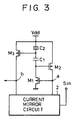
- Fig. 3 shows a comparison detection circuit according to a second embodiment of the present invention.
- the portion of the current mirror circuit 2 is arranged by using the same circuit as that shown in, for example, Fig. 2.
- the different points of this embodiment from those of the first embodiment are that the capacitive unit 5 is formed by connecting the capacitors C1 and C2 in series, the connection point between the capacitors C1 and C2 is connected to the PMOS transistor M3 which acts as an active load, and the other terminal of the capacitor C1 is connected to the PMOS transistor M1 and the PMOS transistor M2 which act as active loads.
- the size ratio of the PMOS transistor M2 to the PMOS transistor M3 may be 1:1.
- the second output terminal b outputs a low-level signal at a level of light (its value is defined by the capacitance ratio of the capacitor C1 to the capacitor C2) smaller than the peak level of light.
- jitter which is a fluctuation of a delay time shown in Fig. 10, can be reduced.
- the inventors of the present invention diligently made an analysis in order to reduce jitter and found that the major factors causing jitter are the following:
- Jitter resulting from the above-described item (1) is the following.
- the delay time ⁇ depends upon a light level Ip, and the delay time ⁇ increases with a decrease in the light level. Therefore, if a light level varies by ⁇ Ip, the delay time ⁇ also varies, that is, jitter occurs.
- an output buffer is provided.
- signal current photocurrent Ip
- this voltage change is transmitted to the output buffer.
- this voltage change exceeds a certain value (slice level)
- the output buffer outputs a signal.
- a power-supply voltage varies, the slice level varies, that is, the slice level has a certain width ⁇ V.
- a voltage change caused by the signal current requires time.
- the time differential of this voltage change is denoted as g
- the jitter can be expressed by ⁇ V/g. If this g is large, jitter becomes small. In the present invention, the delay time ⁇ becomes small. That is, g becomes large, and jitter becomes small.
- Fig. 5 is a circuit diagram illustrating a comparison detection circuit according to a third embodiment of the present invention.
- the comparison detection circuit of Fig. 5 is manufactured as a one-chip, monolithic IC on a silicon semiconductor substrate.
- a very small current source Isl of approximately tens of pA is connected to the gate terminal of the PMOS transistor M2.
- the electrical potential of the gate electrode of the PMOS transistor M2 reaches very close to the power-supply voltage Vdd due to the very small current source Isl. This is a reset state.
- the reset method is not limited to a method using a very small current source, and may be set to a reset electrical potential via a reset switch in accordance with an external or internal reset signal.
- the size ratio of the bipolar transistor T1 for input of the current mirror circuit to the bipolar transistors T2 and T3 for output is 1:5.
- photocurrent generated in the photodiode D flows through the bipolar transistor T1, and electric current which is five times as great as this photocurrent flows through the bipolar transistors T2 and T3.
- photocurrent is 10 ⁇ A
- electric current of 50 ⁇ A can flow through the bipolar transistors T2 and T3.
- the slice level is changed by changing the size ratio of the bipolar transistor T2 to the bipolar transistor T3 without changing the size ratio of the PMOS transistor M2 to the PMOS transistor M3.
- the size ratio of the PMOS transistor M2 to the PMOS transistor M3 is set at 1:1, and the size ratio of the bipolar transistor T2 to the bipolar transistor T3 is set at 10:3.
- the slice level can be made to be 30% of the peak light level in the same way as in the first embodiment.
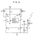
- Fig. 6 is a circuit diagram illustrating a comparison detection circuit according to a fifth embodiment of the present invention.
- an idling current source Is2 is connected to the first output terminal a side of the PMOS transistor M2
- an idling current source Is3 is connected to the second output terminal b side of the PMOS transistor M3
- an idling current source Is4 is connected to the collector side of the bipolar transistor T1.
- a level shift circuit 7 is provided between the PMOS transistor M1 and the first output terminal a.
- This embodiment aims to improve the peak writing accuracy and the rise-time characteristics of the current mirror circuit.
- the size ratio of the bipolar transistor T1 to the bipolar transistors T2 and T3 is set at 1:5, electric current which is five times as great as the current value from the idling current source Is4 is supplied from the idling current sources Is2 and Is3.
- the gate electrical potential of the PMOS transistor M1 is increased to higher than the electrical potential of the output terminal a, and the peak writing accuracy is increased.
- the peak writing accuracy requires that there is no delay between the electrical potential of the first output terminal a and the opening/closing of the switch.
- the electrical potential of the first output terminal a In a case in which there is no level shift, in order for the PMOS transistor M2 to cause electric current to flow, the electrical potential of the first output terminal a must be decreased by an amount of 2Vth of the threshold voltage Vth of the PMOS transistor M2 and the threshold voltage Vth of the PMOS transistor M1 in order to achieve effective writing. Therefore, 2Vth is a wasteful voltage drop, and this amount leads to a delay in the opening/closing of the switch. When a delay occurs in the closing of the switch, writeover occurs. If a shift by an amount of 2Vth is made previously by the level shift circuit, there occurs no wasteful voltage drop, and writeover does not occur.
- Fig. 7 is a circuit diagram illustrating a comparison detection circuit according to a sixth embodiment of the present invention.
- PMOS transistors are not used as active loads, but PNP bipolar transistors T4 and T5 are used.
- the base of the PNP bipolar transistor T4 and the base of the PNP bipolar transistor T5 are connected in common, and the two bases are grounded via the PMOS transistor M4 and connected to Vdd having a relatively large resistance value via a resistor R3.
- the gate of the PMOS transistor M4 is connected to the capacitor C and the PMOS transistor M1.
- the size ratio of the bipolar transistor T1 to the bipolar transistors T2 and T3 is set at 1:5, and the size ratio of the PNP bipolar transistor T4 to the PNP bipolar transistor T5 is set at 10:3. Therefore, the current supply capability of the PNP bipolar transistor T5 becomes 3/10 of that of the PNP bipolar transistor T4.
- the first output terminal a reaches a low level if Ies ⁇ exp (q ⁇ Vbe/kT) ⁇ 5Ip (Condition (1)), and the first output terminal a reaches a high level if Ies ⁇ exp (q ⁇ Vbe/kT) > 5Ip (Condition (2)). Since the PNP bipolar transistor T4 is an active load, the first output terminal a immediately reaches a high level at the moment Condition (2) is satisfied, causing the PMOS transistor M1 to be turned off.
- the current supply capability of the bipolar transistor T5 is 3/10 of that of the PNP bipolar transistor T4.
- Fig. 8 is a schematic view illustrating a laser beam printer (an electrophotographic apparatus using laser light as exposure light) employing a detection circuit according to the present invention.
- a laser light source 101 having a particle laser which emits laser light, a polygon mirror 102, and a mirror 103, which form an exposure optical system, and a photosensitive member 104 and a controller 105.
- the detection circuit of the present invention together with a photo-receiving element, is provided in a horizontal scanning detection circuit 106 in order to synchronize the horizontal scanning timing of one line with the rotation timing of the photosensitive member.
- Laser light emitted from the laser light source 101 is caused to horizontally scan by the polygon mirror 102 and irradiated onto the surface of the photosensitive member 104 via the mirror 103.
- a detection circuit includes a current mirror circuit that produces electric currents at first and second output terminals in response to a current supplied to its input terminal.
- a first active load is connected to the first output terminal and a second active load is connected to the second output terminal and an external output terminal.
- a control circuit controls the potential of the control electrode of the second active load according to the voltage or the current at the first output terminal.
- the control circuit can include a capacitive device that determines the voltage at the control electrodes of the active loads according to the peak value of current supplied to the current mirror circuit input terminal.
Landscapes
- Engineering & Computer Science (AREA)
- Physics & Mathematics (AREA)
- Microelectronics & Electronic Packaging (AREA)
- Nonlinear Science (AREA)
- Electromagnetism (AREA)
- General Physics & Mathematics (AREA)
- Radar, Positioning & Navigation (AREA)
- Automation & Control Theory (AREA)
- Measurement Of Current Or Voltage (AREA)
Applications Claiming Priority (3)
| Application Number | Priority Date | Filing Date | Title |
|---|---|---|---|
| JP1567496 | 1996-01-31 | ||
| JP1567496 | 1996-01-31 | ||
| JP15674/96 | 1996-01-31 |
Publications (2)
| Publication Number | Publication Date |
|---|---|
| EP0788046A1 true EP0788046A1 (de) | 1997-08-06 |
| EP0788046B1 EP0788046B1 (de) | 2001-11-14 |
Family
ID=11895304
Family Applications (1)
| Application Number | Title | Priority Date | Filing Date |
|---|---|---|---|
| EP97101490A Expired - Lifetime EP0788046B1 (de) | 1996-01-31 | 1997-01-30 | Erfassungsschaltung |
Country Status (3)
| Country | Link |
|---|---|
| US (1) | US5801581A (de) |
| EP (1) | EP0788046B1 (de) |
| DE (1) | DE69708167T2 (de) |
Cited By (2)
| Publication number | Priority date | Publication date | Assignee | Title |
|---|---|---|---|---|
| EP0930708A3 (de) * | 1998-01-14 | 2000-10-11 | Canon Kabushiki Kaisha | Analoge Signalverarbeitungsschaltung, Photodetektor und Bilderzeugungsvorrichtung |
| US7466202B2 (en) | 2006-04-07 | 2008-12-16 | Atmel Germany Gmbh | High-speed CMOS current mirror |
Families Citing this family (6)
| Publication number | Priority date | Publication date | Assignee | Title |
|---|---|---|---|---|
| DE19609831A1 (de) * | 1996-03-13 | 1997-09-18 | Philips Patentverwaltung | Schaltungsanordnung zum Liefern eines Gleichstromes |
| US6404241B1 (en) * | 2000-01-13 | 2002-06-11 | Lsi Logic Corporation | Current-Mode Peak Detector |
| US6665339B1 (en) * | 2001-03-19 | 2003-12-16 | Cisco Systems Wireless Networking (Australia) Pty. Limited | Method and apparatus for reducing oscillator pull in a CMOS wireless transceiver integrated circuit |
| US6812686B2 (en) * | 2003-02-21 | 2004-11-02 | Semiconductor Components Industries | Method of forming an RF detector and structure therefor |
| EP2145380B1 (de) * | 2007-04-27 | 2016-01-06 | Koninklijke Philips N.V. | Selbstschwingender schalterstromkreis für einen dc-dc-schaltwandler |
| KR101401528B1 (ko) * | 2007-06-29 | 2014-06-03 | 가부시키가이샤 한도오따이 에네루기 켄큐쇼 | 광전변환장치 및 그 광전변환장치를 구비하는 전자기기 |
Citations (2)
| Publication number | Priority date | Publication date | Assignee | Title |
|---|---|---|---|---|
| EP0288574A1 (de) * | 1986-10-23 | 1988-11-02 | Fanuc Ltd. | Gerät zur verarbeitung von signalen eines pulskodierers |
| EP0661616A2 (de) * | 1993-12-29 | 1995-07-05 | AT&T Corp. | Bandlückenspannungsreferenzgenerator |
-
1997
- 1997-01-23 US US08/786,335 patent/US5801581A/en not_active Expired - Lifetime
- 1997-01-30 DE DE69708167T patent/DE69708167T2/de not_active Expired - Lifetime
- 1997-01-30 EP EP97101490A patent/EP0788046B1/de not_active Expired - Lifetime
Patent Citations (2)
| Publication number | Priority date | Publication date | Assignee | Title |
|---|---|---|---|---|
| EP0288574A1 (de) * | 1986-10-23 | 1988-11-02 | Fanuc Ltd. | Gerät zur verarbeitung von signalen eines pulskodierers |
| EP0661616A2 (de) * | 1993-12-29 | 1995-07-05 | AT&T Corp. | Bandlückenspannungsreferenzgenerator |
Cited By (3)
| Publication number | Priority date | Publication date | Assignee | Title |
|---|---|---|---|---|
| EP0930708A3 (de) * | 1998-01-14 | 2000-10-11 | Canon Kabushiki Kaisha | Analoge Signalverarbeitungsschaltung, Photodetektor und Bilderzeugungsvorrichtung |
| US6410903B1 (en) | 1998-01-14 | 2002-06-25 | Canon Kabushiki Kaisha | Analog signal processing circuit photo detector and image forming apparatus |
| US7466202B2 (en) | 2006-04-07 | 2008-12-16 | Atmel Germany Gmbh | High-speed CMOS current mirror |
Also Published As
| Publication number | Publication date |
|---|---|
| US5801581A (en) | 1998-09-01 |
| HK1001794A1 (en) | 1998-07-10 |
| DE69708167D1 (de) | 2001-12-20 |
| DE69708167T2 (de) | 2002-06-20 |
| EP0788046B1 (de) | 2001-11-14 |
Similar Documents
| Publication | Publication Date | Title |
|---|---|---|
| US5442277A (en) | Internal power supply circuit for generating internal power supply potential by lowering external power supply potential | |
| US5861621A (en) | Photosensor circuit having an initial setting unit | |
| US5233180A (en) | Light sensor having an integration circuit | |
| JP2761687B2 (ja) | 電圧レベル検出回路 | |
| EP0747800B1 (de) | Schaltungsanordnung zum Liefern einer kompensierten Polarisationsspannung für P-Kanal-Transistoren | |
| US4368420A (en) | Supply voltage sense amplifier | |
| GB2248357A (en) | Source voltage control circuit | |
| US5276359A (en) | Current-input type interface circuit of a mouse | |
| JP2009080653A (ja) | 半導体集積回路装置 | |
| JPH02183126A (ja) | 温度閾値検知回路 | |
| EP0788046B1 (de) | Erfassungsschaltung | |
| US4464591A (en) | Current difference sense amplifier | |
| US5955891A (en) | Semiconductor integrated circuit device with output circuit | |
| US5731735A (en) | Power supply circuit for driving an integrated circuit, wherein the power supply is adjusted based on temperature so that a delay variation within the IC according to temperature may be cancelled | |
| KR960013863B1 (ko) | 레벨 변환 회로 | |
| JP3461257B2 (ja) | 検出回路およびこの検出回路を用いた装置 | |
| EP0738038B1 (de) | Stromverstärker | |
| EP0930708B1 (de) | Analoge Signalverarbeitungsschaltung, Photodetektor und Bilderzeugungsvorrichtung | |
| US6297492B1 (en) | Fast BICMOS active-pixel sensor cell with fast NPN emitter-follower readout | |
| HK1001794B (en) | Detection circuit | |
| JPH0553406B2 (de) | ||
| US5225716A (en) | Semiconductor integrated circuit having means for suppressing a variation in a threshold level due to temperature variation | |
| EP0460273A1 (de) | Verstärkungsstabilisierter Verstärker | |
| EP0477088B1 (de) | Integrierte Halbleiterschaltung mit Mitteln zur Unterdrückung von temperaturabhängigen Schwellenschwankungen | |
| US4626793A (en) | Receiver amplifier for amplification of a photoelectric current |
Legal Events
| Date | Code | Title | Description |
|---|---|---|---|
| PUAI | Public reference made under article 153(3) epc to a published international application that has entered the european phase |
Free format text: ORIGINAL CODE: 0009012 |
|
| AK | Designated contracting states |
Kind code of ref document: A1 Designated state(s): DE FR GB IT |
|
| 17P | Request for examination filed |
Effective date: 19971223 |
|
| 17Q | First examination report despatched |
Effective date: 19991203 |
|
| GRAG | Despatch of communication of intention to grant |
Free format text: ORIGINAL CODE: EPIDOS AGRA |
|
| GRAG | Despatch of communication of intention to grant |
Free format text: ORIGINAL CODE: EPIDOS AGRA |
|
| GRAG | Despatch of communication of intention to grant |
Free format text: ORIGINAL CODE: EPIDOS AGRA |
|
| GRAH | Despatch of communication of intention to grant a patent |
Free format text: ORIGINAL CODE: EPIDOS IGRA |
|
| GRAH | Despatch of communication of intention to grant a patent |
Free format text: ORIGINAL CODE: EPIDOS IGRA |
|
| GRAA | (expected) grant |
Free format text: ORIGINAL CODE: 0009210 |
|
| AK | Designated contracting states |
Kind code of ref document: B1 Designated state(s): DE FR GB IT |
|
| REF | Corresponds to: |
Ref document number: 69708167 Country of ref document: DE Date of ref document: 20011220 |
|
| REG | Reference to a national code |
Ref country code: GB Ref legal event code: IF02 |
|
| PLBE | No opposition filed within time limit |
Free format text: ORIGINAL CODE: 0009261 |
|
| STAA | Information on the status of an ep patent application or granted ep patent |
Free format text: STATUS: NO OPPOSITION FILED WITHIN TIME LIMIT |
|
| 26N | No opposition filed | ||
| PGFP | Annual fee paid to national office [announced via postgrant information from national office to epo] |
Ref country code: IT Payment date: 20090116 Year of fee payment: 13 |
|
| PGFP | Annual fee paid to national office [announced via postgrant information from national office to epo] |
Ref country code: FR Payment date: 20090121 Year of fee payment: 13 |
|
| REG | Reference to a national code |
Ref country code: FR Ref legal event code: ST Effective date: 20100930 |
|
| PG25 | Lapsed in a contracting state [announced via postgrant information from national office to epo] |
Ref country code: FR Free format text: LAPSE BECAUSE OF NON-PAYMENT OF DUE FEES Effective date: 20100201 |
|
| PG25 | Lapsed in a contracting state [announced via postgrant information from national office to epo] |
Ref country code: IT Free format text: LAPSE BECAUSE OF NON-PAYMENT OF DUE FEES Effective date: 20100130 |
|
| PGFP | Annual fee paid to national office [announced via postgrant information from national office to epo] |
Ref country code: DE Payment date: 20150131 Year of fee payment: 19 |
|
| PGFP | Annual fee paid to national office [announced via postgrant information from national office to epo] |
Ref country code: GB Payment date: 20150123 Year of fee payment: 19 |
|
| REG | Reference to a national code |
Ref country code: DE Ref legal event code: R119 Ref document number: 69708167 Country of ref document: DE |
|
| GBPC | Gb: european patent ceased through non-payment of renewal fee |
Effective date: 20160130 |
|
| PG25 | Lapsed in a contracting state [announced via postgrant information from national office to epo] |
Ref country code: GB Free format text: LAPSE BECAUSE OF NON-PAYMENT OF DUE FEES Effective date: 20160130 Ref country code: DE Free format text: LAPSE BECAUSE OF NON-PAYMENT OF DUE FEES Effective date: 20160802 |