EP0788112A2 - Speicher-Adressierschaltung - Google Patents
Speicher-Adressierschaltung Download PDFInfo
- Publication number
- EP0788112A2 EP0788112A2 EP97300611A EP97300611A EP0788112A2 EP 0788112 A2 EP0788112 A2 EP 0788112A2 EP 97300611 A EP97300611 A EP 97300611A EP 97300611 A EP97300611 A EP 97300611A EP 0788112 A2 EP0788112 A2 EP 0788112A2
- Authority
- EP
- European Patent Office
- Prior art keywords
- address
- line
- output
- input
- lines
- Prior art date
- Legal status (The legal status is an assumption and is not a legal conclusion. Google has not performed a legal analysis and makes no representation as to the accuracy of the status listed.)
- Withdrawn
Links
Images


Classifications
-
- G—PHYSICS
- G11—INFORMATION STORAGE
- G11C—STATIC STORES
- G11C11/00—Digital stores characterised by the use of particular electric or magnetic storage elements; Storage elements therefor
- G11C11/21—Digital stores characterised by the use of particular electric or magnetic storage elements; Storage elements therefor using electric elements
- G11C11/34—Digital stores characterised by the use of particular electric or magnetic storage elements; Storage elements therefor using electric elements using semiconductor devices
- G11C11/40—Digital stores characterised by the use of particular electric or magnetic storage elements; Storage elements therefor using electric elements using semiconductor devices using transistors
- G11C11/401—Digital stores characterised by the use of particular electric or magnetic storage elements; Storage elements therefor using electric elements using semiconductor devices using transistors forming cells needing refreshing or charge regeneration, i.e. dynamic cells
- G11C11/4063—Auxiliary circuits, e.g. for addressing, decoding, driving, writing, sensing or timing
- G11C11/407—Auxiliary circuits, e.g. for addressing, decoding, driving, writing, sensing or timing for memory cells of the field-effect type
-
- G—PHYSICS
- G11—INFORMATION STORAGE
- G11C—STATIC STORES
- G11C7/00—Arrangements for writing information into, or reading information out from, a digital store
- G11C7/10—Input/output [I/O] data interface arrangements, e.g. I/O data control circuits, I/O data buffers
- G11C7/1015—Read-write modes for single port memories, i.e. having either a random port or a serial port
- G11C7/1018—Serial bit line access mode, e.g. using bit line address shift registers, bit line address counters, bit line burst counters
-
- G—PHYSICS
- G11—INFORMATION STORAGE
- G11C—STATIC STORES
- G11C8/00—Arrangements for selecting an address in a digital store
- G11C8/04—Arrangements for selecting an address in a digital store using a sequential addressing device, e.g. shift register, counter
Definitions
- the subject invention relates to a system for addressing cells of a memory array.
- a DRAM system (a memory system using DRAM cells) comprises a DRAM cell array 1 (memory array constituted by DRAM cells) which is a region for storing information, and an address decoder for accessing a designated address.
- the DRAM array 1 is formed in a matrix in which DRAM cells are arranged in a grid.
- a specific DRAM cell 4 is identified by an address allocated to a row and a column of the matrix.
- the address is externally supplied from a CPU or the like as an input address 10 of a bit string with predetermined number of bits, and divided into bit strings with predetermined number of bits, respectively, for a row predecoder 11 and a column predecoder 12.
- the input address 10 is 16 bits long, 11 bits of which are input into the row predecoder 11, and the remaining bits of which are input into the column predecoder 12.
- it varies depending on the structure of the DRAM array 1.
- Parts of the respective addresses supplied to the row predecoder 11 and the column predecoder 12 are decoded (predecoded). Then, the predecoded addresses are supplied to a row decoder 2 and a column decoder 3 directly connected to the DRAM array 1, respectively, where they are decoded to generate a final address. A desired bit 4 is accessed from a desired address in the DRAM array 1 with the generated address. It is well known in the art relating to a DRAM that the input address is thus decoded in several steps.
- Figure 2 shows detail of the column predecoder 12.
- the column predecoder 12 is input with five-bit signals from AC0 - AC4 of a bit string relating to the input address 10. These signals are predecoded by predecoder means 13, 14, and 15. For example, AC0 and AC1 are converted to any one output of BY0 - BY3 by the predecoder means 13.
- AC2 and AC3 are also converted to any one output of BY4 - BY7 by the predecoder means 14, and AC4 is also converted to either one of BY8 or BY9 by the predecoder means 15.
- Figure 3 shows detail of the column decoder 3. Any one of 32 bit lines is selected by three inputs, namely any one output of BY0 - BY3 (corresponding to AC0 and AC1 of the input address), any one output of BY4 - BY7 (corresponding to AC2 and AC3 of the input address), and either one output of BY8 or BY9 (corresponding to AC4 of the input address).
- the burst mode means a mode in which data relating to a plurality of contiguous (consecutive) column addresses are continuously input or output every clock cycle. This mode is frequently used as a scheme for complementing the low operating speed which the DRAM inherently has because this mode allows input and output at a high speed for a case of image data in which data is stored in contiguous physical addresses.
- the predecessor to the burst mode is a mode called nibble mode.
- the nibble mode burst outputs four bits stored at contiguous column addresses.
- the circuit is configured in such a manner that the addresses vary as the electric potential of CAS is increased or decreased (cycled). Then, a normal accessing method is used for one bit first accessed (and, therefore, requiring a relatively long period of time), and succeeding three bits are continuously burst output by cycling CAS.
- this scheme allows burst output at a high speed, since higher bits in the input address are fixed, addressing merely cycles in addresses in a unit of four bits. In other words, burst input/output cannot be performed across bit line groups.
- bit lines are grouped into four-bit lines each by AC0 and AC1 which are the lower two bits of the input address bits.
- One of these bit line groups is called a block in the following.
- the burst mode is an improvement of the nibble mode. Unlike the nibble mode, the burst mode can access addresses in the cycle in various sequences. To perform continuous burst input/output, it is necessary to select the bit lines contiguously arranged by means of a clock cycle. Doing this becomes difficult if addresses are externally input every time. Accordingly, a technology has been developed that, when an address is first input, for example, succeeding inputs are automatically generated within a DRAM system to allow continuous burst input/output. In this technology, for example, an address counter is prepared in a DRAM to detect at which number of access that access is made in the burst mode. Then, an address is generated at timing synchronizing an external clock according to the number of accesses detected by the address counter. However, even in the presently known burst mode, output cannot be performed across blocks.
- the background art has a disadvantage that the burst output cannot be performed across blocks. This adversely affects speed of DRAM operation in that, if it is desired, for example, in Figure 3 to continuously output data relating to bit lines 6, 7, 8, and 9, it is necessary to perform burst output two times, and to discard data relating to unnecessary bit lines 4, 5, 10, and 11.
- the present invention provides a memory addressing circuit for addressing cells of a memory array including respective pluralities of row and column address lines, activation of one of each type of address line addressing uniquely a corresponding cell of the memory, and decoding means for decoding an address expressed in a binary coded notation to select and activate one of said address lines, characterised in that a shifting means is provided responsive to at least one additional input signal to modify the operation of the decoding means so as to select and activate an additional address line simultaneously with said primary selected address line.
- the subject invention has the advantage of providing an addressing system which allows selection of any contiguous column addresses across blocks.
- a predecoder circuit is employed.
- the predecoder circuit is utilized in an environment where a plurality of address lines are divided into blocks consisting of a predetermined number of address lines. These blocks are defined by a higher bit string of bit string relating to the input address. It is a final object to simultaneously select a first address line and a second address line from the address lines contained in the address line group defined by the higher bit of bit string by the lower bit string relating to the input address.
- the predecoder circuit according to the subject invention comprises at least numbered output lines in the number corresponding to the number of bits in the lower bit string of an input address input therein, and a designating input for designating the relationship, which is either larger or smaller, between a first address corresponding to the first address line to be selected and a second address corresponding to the second address line.
- the operation of the predecoder circuit according to the subject invention is divided into the following occasions.
- the designating input designates that the second address corresponding to the second address line is smaller than the first address corresponding to the first address line, it can be considered to be similar to the above.
- the designating input designates that the second address is smaller than the first address, it is preferable that corresponding signals are activated, and other signals in complementary relationship to these signals are provided. This will be described in detail for the embodiment in the following.
- a decoder circuit is required to be connected between the predecoder circuit and the DRAM array.
- the decoder circuit is to simultaneously select a first address line and a second address line adjacent to the first address line and having a larger numbering than it from the address line group divided into a plurality of groups by a lower bit string relating to the input address.
- the decoder circuit according to the subject invention comprises a plurality of input lines to which signal lines output by a predecoder circuit are input, a first input line for inputting a signal indicating shift-up, a second input line complementary to the first input line, and a plurality of address lines.
- the decoder circuit selects, when a first address corresponding to the first address line is the largest in its group, selects a second address line corresponding to the smallest address in a higher group adjacent to that group.
- a line extends from the original group to the adjacent higher group, and activated by the first input line indicating shift-up.
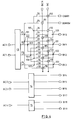
- the predecoder according to the subject invention is shown in Figure 4. Differences from the predecoder according to the background art as shown in Figure 2 lie in that INC and INCN signals are input into the predecoder means 13 associated with AC0 and AC1 which are bit strings relating to the lower two bits of the input address, that CARRY and BORROW signals are output, and a new arrangement of connection is made between lines due to introduction of these new signals.
- INC and INCN have complementary values that is, the inverse of each other. That is, if the former is high, the latter is low, or vice versa. In this case, when INC is high, it indicates that an address relating to the address being input is incremented by one to designate a second bit line. In addition, when INC is low, INCN is high, and it indicates that an address relating to the address being input is decremented by one to designate a second bit line. INC and INCN are designated by a user input.
- CARRY is an output signal for selecting a bit line from a higher block adjacent to the block defined by the input address
- BORROW is an output signal for selecting a bit line from a lower block adjacent to the block defined by the input address. In the drawing, contact points between lines are indicated by a symbol or O.
- the line 26 is connected to BY0 through a contact 120. Accordingly, the first output becomes BY0 as per the input address.
- a contact 114 with INC is conductive because INC is higher. Accordingly, the line 27 is connected to BY1 (input address + 1) through contacts 114 and 121.
- the predecoder according to the subject invention simultaneously outputs an output as per the input address and an output incremented by + 1 with respect to the input address.
- the predecoder according to the subject invention simultaneously outputs an output as per the input address and an output incremented by + 1 with respect to the input address.
- INCN high.
- the line 23 is selected, and connected to the lines 32, 33, and 34 through the contact 104.
- the line 33 outputs BY2 (as per the input address) through the contact 122.
- the line 34 is shut down because it is not connected to INCN, and only the line 32 outputs BY1 (input address - 1) through the contact 115 connected to INCN and the contact 121.
- the predecoder according to the subject invention simultaneously outputs an output as per the input address and an output decremented by - 1 with respect to the input address.
- the predecoder according to the subject invention can simultaneously output any adjacent two of outputs of BY0 - BY3 in the same block.
- the lines 35 and 36 output CARRY and BY0 through the contacts 110 and 112, and through the contact 120, respectively, because both of them are connected to INC.
- Simultaneous output of CARRY and BYO is the second output at the time of predecoding.
- CARRY is an output signal designating an adjacent higher block
- the second output consequently designates BY0 of the adjacent higher block.
- an address and INCN out of the range of the same block are designated.
- the first output as per the input address should be BY0 of the designated block
- the second output should be BY3 of an adjacent lower block.
- the line 21 is first selected.
- the line 21 is connected to the lines 25, 26, 27, and 28 through the contacts 101 and 102.
- the line 27 is shut down because it is not connected to INCN.
- the line 26 outputs BY0 as the first output through the contact 120 (as per the input address).
- the lines 25 and 26 are connected to INCN through the contacts 111 and 119, and output BORROW and BY3 as the second output through the contact 123, respectively. Therefore, in this case also, the second output becomes simultaneous output of BORROW and BY3.
- BORROW is an output signal designating an adjacent lower block, and the second output consequently designates BY3 of the adjacent lower block.
- the predecoder according to the subject invention simultaneously outputs an output as per the input address and an output of the input address - 1 (actually, an address contained in the adjacent lower block) with one input address. This is because BORROW for shifting down to the adjacent lower block is simultaneously output together with the second output.
- Figure 5 shows a column decoder according to the subject invention.
- the column decoder inputs are the outputs of the predecoder shown in Figure 4.
- the column decoder according to the subject invention differs from that according to the background art as shown in Figure 3 in that the output signals CARRY, CARRYN, BORROW, and BORROWN from the predecoder are input into the decoder, and that arrangement of connection between these input signals and respective bit lines is novel.
- CARRY and CARRYN, and BORROW and BORROWN are complementary to each other. Accordingly, if the former is high, the latter automatically outputs a low signal, and vice versa.
- the input address and an adjacent column address larger or smaller than the input address by one can be selected as the first output and the second output, respectively.
- INC and INCN are provided for the above-mentioned embodiment, provision of only one of them does not impair attainment of the object of the subject invention.
Landscapes
- Engineering & Computer Science (AREA)
- Microelectronics & Electronic Packaging (AREA)
- Computer Hardware Design (AREA)
- Dram (AREA)
- Static Random-Access Memory (AREA)
Applications Claiming Priority (2)
| Application Number | Priority Date | Filing Date | Title |
|---|---|---|---|
| JP01893096A JP3247603B2 (ja) | 1996-02-05 | 1996-02-05 | プレデコーダ回路及びデコーダ回路 |
| JP18930/96 | 1996-02-05 |
Publications (2)
| Publication Number | Publication Date |
|---|---|
| EP0788112A2 true EP0788112A2 (de) | 1997-08-06 |
| EP0788112A3 EP0788112A3 (de) | 1999-01-27 |
Family
ID=11985364
Family Applications (1)
| Application Number | Title | Priority Date | Filing Date |
|---|---|---|---|
| EP97300611A Withdrawn EP0788112A3 (de) | 1996-02-05 | 1997-01-30 | Speicher-Adressierschaltung |
Country Status (4)
| Country | Link |
|---|---|
| US (1) | US5805521A (de) |
| EP (1) | EP0788112A3 (de) |
| JP (1) | JP3247603B2 (de) |
| KR (1) | KR100218201B1 (de) |
Families Citing this family (3)
| Publication number | Priority date | Publication date | Assignee | Title |
|---|---|---|---|---|
| KR20030082548A (ko) * | 2000-11-28 | 2003-10-22 | 시체인지 인터내셔널, 인코포레이티드 | 콘텐츠/서비스 처리 및 전달 |
| US6714467B2 (en) * | 2002-03-19 | 2004-03-30 | Broadcom Corporation | Block redundancy implementation in heirarchical RAM's |
| KR100543448B1 (ko) * | 2003-04-03 | 2006-01-23 | 삼성전자주식회사 | 버스트 읽기 동작 모드를 갖는 플래시 메모리 장치 |
Family Cites Families (8)
| Publication number | Priority date | Publication date | Assignee | Title |
|---|---|---|---|---|
| JP3231842B2 (ja) * | 1992-06-23 | 2001-11-26 | 株式会社 沖マイクロデザイン | シリアルアクセスメモリ |
| JPH0636560A (ja) * | 1992-07-21 | 1994-02-10 | Mitsubishi Electric Corp | 半導体記憶装置 |
| KR960001859B1 (ko) * | 1993-04-16 | 1996-02-06 | 삼성전자주식회사 | 반도체 메모리장치의 디코딩회로 및 그 방법 |
| KR100309800B1 (ko) * | 1993-11-08 | 2001-12-15 | 윤종용 | 동기랜덤액세스메모리장치 |
| US5574880A (en) * | 1994-03-11 | 1996-11-12 | Intel Corporation | Mechanism for performing wrap-around reads during split-wordline reads |
| JP2982618B2 (ja) * | 1994-06-28 | 1999-11-29 | 日本電気株式会社 | メモリ選択回路 |
| US5513139A (en) * | 1994-11-04 | 1996-04-30 | General Instruments Corp. | Random access memory with circuitry for concurrently and sequentially writing-in and reading-out data at different rates |
| US5586080A (en) * | 1995-06-26 | 1996-12-17 | Micron Technology, Inc. | Local word line phase driver |
-
1996
- 1996-02-05 JP JP01893096A patent/JP3247603B2/ja not_active Expired - Fee Related
- 1996-11-15 KR KR1019960055505A patent/KR100218201B1/ko not_active Expired - Fee Related
- 1996-12-26 US US08/773,150 patent/US5805521A/en not_active Expired - Fee Related
-
1997
- 1997-01-30 EP EP97300611A patent/EP0788112A3/de not_active Withdrawn
Also Published As
| Publication number | Publication date |
|---|---|
| US5805521A (en) | 1998-09-08 |
| JP3247603B2 (ja) | 2002-01-21 |
| JPH09213075A (ja) | 1997-08-15 |
| KR100218201B1 (ko) | 1999-09-01 |
| KR970063260A (ko) | 1997-09-12 |
| EP0788112A3 (de) | 1999-01-27 |
Similar Documents
| Publication | Publication Date | Title |
|---|---|---|
| US5485418A (en) | Associative memory | |
| US5390149A (en) | System including a data processor, a synchronous dram, a peripheral device, and a system clock | |
| US4467443A (en) | Bit addressable variable length memory system | |
| EP0473275B1 (de) | Speichersteuerungseinheit und Speichereinheit | |
| US5752260A (en) | High-speed, multiple-port, interleaved cache with arbitration of multiple access addresses | |
| US5341486A (en) | Automatically variable memory interleaving system | |
| US5396608A (en) | Method and apparatus for accessing variable length words in a memory array | |
| US4773049A (en) | Semiconductor memory device having improved access time for continuously accessing data | |
| US4593373A (en) | Method and apparatus for producing n-bit outputs from an m-bit microcomputer | |
| US4800535A (en) | Interleaved memory addressing system and method using a parity signal | |
| US6553478B1 (en) | Computer memory access | |
| EP0788112A2 (de) | Speicher-Adressierschaltung | |
| KR0167629B1 (ko) | 순차 액세스 동작을 수행하는 메모리 회로 | |
| US5577221A (en) | Method and device for expanding ROM capacity | |
| US5860076A (en) | 48-bit wide memory architecture addressing scheme reconfigurable for 8-bit, 16-bit and 32-bit data accesses | |
| US5089987A (en) | Refresh control circuit | |
| US5875147A (en) | Address alignment system for semiconductor memory device | |
| US6742077B1 (en) | System for accessing a memory comprising interleaved memory modules having different capacities | |
| CN100375065C (zh) | 产生预测地址值的电路和方法 | |
| US5241665A (en) | Memory bank comparator system | |
| JP3540388B2 (ja) | コンピュータシステム | |
| US6502179B2 (en) | Method and apparatus for compactly storing instruction codes | |
| EP0473274B1 (de) | Speicherbankvergleichseinrichtung | |
| KR100215903B1 (ko) | 메모리의리드/라이트회로 | |
| RU2115160C1 (ru) | Устройство динамического изменения адресов памяти |
Legal Events
| Date | Code | Title | Description |
|---|---|---|---|
| PUAI | Public reference made under article 153(3) epc to a published international application that has entered the european phase |
Free format text: ORIGINAL CODE: 0009012 |
|
| AK | Designated contracting states |
Kind code of ref document: A2 Designated state(s): DE FR GB |
|
| PUAL | Search report despatched |
Free format text: ORIGINAL CODE: 0009013 |
|
| AK | Designated contracting states |
Kind code of ref document: A3 Designated state(s): DE FR GB |
|
| 17P | Request for examination filed |
Effective date: 19990724 |
|
| STAA | Information on the status of an ep patent application or granted ep patent |
Free format text: STATUS: THE APPLICATION HAS BEEN WITHDRAWN |
|
| 18W | Application withdrawn |
Withdrawal date: 19991229 |