EP0788165A2 - Système de cellules de mémoire et son procédé de fabrication - Google Patents
Système de cellules de mémoire et son procédé de fabrication Download PDFInfo
- Publication number
- EP0788165A2 EP0788165A2 EP96119225A EP96119225A EP0788165A2 EP 0788165 A2 EP0788165 A2 EP 0788165A2 EP 96119225 A EP96119225 A EP 96119225A EP 96119225 A EP96119225 A EP 96119225A EP 0788165 A2 EP0788165 A2 EP 0788165A2
- Authority
- EP
- European Patent Office
- Prior art keywords
- mos transistors
- trenches
- memory cell
- cell arrangement
- layer
- Prior art date
- Legal status (The legal status is an assumption and is not a legal conclusion. Google has not performed a legal analysis and makes no representation as to the accuracy of the status listed.)
- Granted
Links
Images


Classifications
-
- H—ELECTRICITY
- H10—SEMICONDUCTOR DEVICES; ELECTRIC SOLID-STATE DEVICES NOT OTHERWISE PROVIDED FOR
- H10B—ELECTRONIC MEMORY DEVICES
- H10B20/00—Read-only memory [ROM] devices
- H10B20/27—ROM only
- H10B20/50—ROM only having transistors on different levels, e.g. 3D ROM
-
- H—ELECTRICITY
- H10—SEMICONDUCTOR DEVICES; ELECTRIC SOLID-STATE DEVICES NOT OTHERWISE PROVIDED FOR
- H10B—ELECTRONIC MEMORY DEVICES
- H10B20/00—Read-only memory [ROM] devices
Definitions
- MOS transistors Semiconductor-based read-only memories are known for storing smaller amounts of data. These are often implemented as a planar integrated silicon circuit in which MOS transistors are used as memory cells. The transistors are selected via the gate electrode which is connected to the word line. The input of the MOS transistor is connected to a reference line, the output to a bit line. The reading process evaluates whether a current flows through the transistor or not. The logical values zero and one are assigned accordingly. Technically, the storage of zero and one is effected in that in memory cells in which the state no current flow through the transistor "assigned logical value is stored, no MOS transistor is produced or no conductive connection to the bit line is realized. Alternatively, MOS transistors can be realized for the two logical values, which have different threshold voltages due to different implantations in the channel area.
- semiconductor-based memories allow random access to the stored information.
- the one for reading the The electrical power required for information is significantly smaller than in the aforementioned storage systems with mechanically moving parts. Since no moving parts are required, mechanical wear and sensitivity to vibrations are also eliminated.
- Semiconductor-based memories can therefore also be used for mobile systems.
- the silicon memories described have a planar structure. This means that a minimum space requirement is required per memory cell, which in the best case is 4 F 2 , where F is the smallest structure size that can be produced in the respective technology.
- a read-only memory cell arrangement is known from DE 42 14 923 A1, the memory cells of which comprise MOS transistors. These MOS transistors are arranged along trenches such that a source region adjoins the bottom of the trench, a drain region adjoins the surface of the substrate and a channel region both vertically to the surface of the substrate and parallel to the surface of the substrate at the flank and bottom of the trench adjacent.
- the surface of the channel area is provided with a gate dielectric.
- the gate electrode is designed as a flank covering (spacer).
- the logical values zero and one are distinguished by different threshold voltages that are caused by channel implantation. In the case of channel implantation, the implanting ions hit the surface of the respective trench at such an angle that shadowing effects on the opposite flank are used to implant only along one flank.
- the invention is based on the problem of specifying a memory cell arrangement based on semiconductors, in which an increased storage density is achieved, so that it is suitable as a read memory for large amounts of data, and which can be produced with few production steps and high yield. Furthermore, a method for producing such a memory cell arrangement is to be specified.
- the memory cell arrangement according to the invention is implemented in a semiconductor substrate.
- a substrate which has monocrystalline silicon at least in the region of a main surface is preferably used as the semiconductor substrate. Both a monocrystalline silicon wafer and an SOI substrate are suitable as the semiconductor substrate.
- the memory cell arrangement has a multiplicity of memory cells, each of which comprises at least one MOS transistor.
- First memory cells include planar MOS transistors, which are arranged in parallel lines. In the main surface of the semiconductor substrate, essentially parallel, strip-shaped trenches are provided, which run parallel to the rows. The rows are arranged alternately on the bottom of the trenches and on the main area between adjacent trenches.
- Second memory cells include vertical MOS transistors on the main surface, which are each implemented on the side walls of the trenches.
- the first memory cells and the second memory cells differ with regard to the technological design of the MOS transistor. With regard to the storage options, however, the first memory cells and the second memory cells are equivalent.
- the memory cell arrangement in the production of the memory cell arrangement by producing the MOS transistors with different threshold voltages. This is preferably done by masked channel implantation, in which the doping in the channel region of the MOS transistors is specifically changed.
- different threshold voltages of the MOS transistors are realized in that the MOS transistors, depending on the information stored, have gate dielectrics of different thicknesses. This takes advantage of the fact that if the thickness of the gate dielectrics differs by a factor of 10 or more, the threshold voltages of the MOS transistors differ so clearly that when a selection signal with a level between the two threshold voltages is applied, the one MOS transistor conducts and the one with does not conduct the thicker gate dielectric.
- the MOS transistors have more than two different threshold voltages, depending on the information stored.
- a gate dielectric made of a material with adhesion points for the MOS transistors.
- Detention areas English traps, have the property Capture charge carriers, especially electrons.
- the MOS transistors are wired in such a way that the charge carriers corresponding to the information to be stored enter the gate dielectric and are held in place by the traps.
- This memory cell arrangement is programmed after production by injection of electrons. This can be done by Fowler-Nordheim tunnels as well as by hot electron injection.
- the MOS transistors are programmed so that they have two different threshold voltages. If the memory cell arrangement is to be used for value-added logic, then the gate dielectric is subjected to different charge quantities by appropriate voltage and time conditions during programming in such a way that the MOS transistors have more than two different threshold voltages, depending on the information stored.
- the gate dielectric is designed as a multiple layer, in which at least one layer is provided which has an increased charge carrier cross-section in comparison with at least one further layer in the multiple layer.
- the traps are located at the interface between the two layers.
- the dielectric multilayer preferably comprises an SiO 2 layer, an Si 3 N 4 layer and an SiO 2 layer (so-called ONO).
- the gate dielectric can be a multilayer made of other materials, the layer with the increased charge carrier capture cross section consisting, for example, of Si 3 N 4 , Ta 2 O 5 , Al 2 O 3 or TiO 2 and the adjacent layer of SiO 2 , Si 3 N 4 or Al 2 O 3 .
- the multilayer can comprise more or less than two layers.
- the gate dielectric can comprise a dielectric layer, for example made of SiO 2 , into which foreign atoms for example, W, Pt, Cr, Ni, Pd, Si or Ir are embedded.
- the embedded foreign atoms can be introduced by implantation, by addition during oxidation or by diffusion. In this case, the embedded foreign atoms form the detention points.
- planar MOS transistors arranged in one row are preferably connected in series. Interconnected source / drain regions of planar MOS transistors adjacent along a row are formed as a coherent, doped region.
- the two source / drain regions of each of the vertical MOS transistors are each with one of the source / drain regions of one of the planar MOS transistors on the main surface of the substrate and with one of the source / drain regions of the planar MOS transistors on the bottom the trenches are formed as a continuous doped area.
- the trenches are formed with a width F and a distance F, where F is the smallest structure size that can be produced in the respective technology, and the dimension of the source / drain regions and the channel region of the planar MOS transistors in the direction of the rows chosen in accordance with F, a first memory cell with a planar MOS transistor and a second memory cell with a vertical MOS transistor are arranged on an area of 2 F 2 .
- the average space requirement per memory cell is therefore 1 F 2 .
- This increased packing density is achieved in that the vertical MOS transistors are arranged on the side walls of the trenches and do not require any additional area in the projection onto the main area.
- the planar MOS transistors arranged along adjacent rows are insulated from one another by the channel region of the vertical MOS transistors arranged on the respective side wall.
- a plurality of first word lines are provided, which run transversely to the trenches and which are connected to gate electrodes of planar MOS transistors arranged along different lines.
- a plurality of second word lines are provided, which are each arranged in pairs in one of the trenches.
- the gate electrodes of vertical MOS transistors arranged along one of the side walls of the trenches are connected to one of the second word lines.
- An insulation structure is provided between each two adjacent vertical MOS transistors, which are arranged on the same side wall, which suppresses the formation of conductive channels between adjacent MOS transistors.
- the insulation structures are preferably formed as a doped region in the respective side wall.
- the dopant concentration in the doped region is so high that the parasitic MOS transistor formed between adjacent MOS transistors does not conduct when a voltage is applied to the relevant word line.
- the insulation structures can also be formed as insulating spacers, for example made of SiO 2 .
- the memory cell arrangement can be implemented both with enhancement MOS transistors and with depletion MOS transistors.
- depletion MOS transistors In the case of depletion MOS transistors, however, negative drive voltages are required for effective leakage current suppression.
- enhancement MOS transistors When using enhancement MOS transistors, effective leakage current suppression is achieved even when using positive drive voltages.
- the memory cell arrangement according to the invention is preferably produced using self-adjusting process steps, so that the space requirement per memory cell is reduced.
- stripe-shaped, parallel trenches are etched in the main surface of the semiconductor substrate.
- the vertical MOS transistors are formed in the side walls of the trenches, the planar MOS transistors on the bottom of the trenches and between adjacent trenches on the main surface.
- First word lines running transverse to the trenches are preferably formed.
- the first word lines act as a mask.
- the second word lines are preferably formed as spacers from, for example, doped polysilicon on the side walls of the trenches.
- the surface of the second word lines is covered with insulating material before the first word lines are formed. This is done, for example, by thermal oxidation of the surface, for example when a gate oxide is formed, or by forming insulating spacers, for example from SiO 2 .
- the use of insulating spacers for insulation between the first word lines and the second word lines has the advantage that the insulating spacers can be produced with a greater thickness and independently of other process parameters such as, for example, the gate oxide thickness.
- an insulation region which defines a cell field for the memory cell arrangement (not shown) is first produced in a substrate 1 made of, for example, monocrystalline silicon on a main surface 2 of the substrate 1.
- the isolation area is formed, for example, by a LOCOS process or an STI (Shallow Trench Isolation) process.
- the substrate 1 is, for example, p-doped with a dopant concentration of 10 15 cm -3 .
- the depletion channels 3 are formed with the aid of a first channel implantation with arsenic with an energy of, for example, 40 keV and a dose of 4 ⁇ 10 13 cm -2 .
- the extent of the depletion channels 3 parallel to the main surface 2 is 2 F x 2 F, that is, for example 0.8 ⁇ m x 0.8 ⁇ m when using 0.4 ⁇ m technology (see FIG. 1).
- a trench mask 4 is formed by depositing an SiO 2 layer in a thickness of, for example, 100 nm to 200 nm using a TEOS method and then structuring the SiO 2 layer using photolithographic methods (see FIG. 2).
- strip-shaped trenches 5 are etched using the trench mask 4 as the etching mask.
- the trenches 5 have a depth of, for example, 0.5 ⁇ m.
- the width of the trenches 5 is F, for example 0.4 ⁇ m, the distance between adjacent trenches 5 is also F, for example 0.4 ⁇ m.
- the length of the trenches 5 depends on the size of the memory cell arrangement and is, for example, 130 ⁇ m.
- the width of the depletion channels 3 is set to the spacing of the trenches 5 during the etching of the trenches 5. thats why the adjustment of the trench mask 4 relative to the depletion channels 3 is not critical.
- a first resist mask 6 is then formed using photolithographic process steps (see FIG. 3, FIG. 4, FIG. 5).
- the first paint mask 6 has strip-shaped openings which run perpendicular to the trenches 5 (see supervision in FIG. 3).
- the width of the openings is F, for example 0.4 ⁇ m, the distance between adjacent openings is also F, for example 0.4 ⁇ m.
- insulation structures 7 are produced on the side walls of the trenches.
- the isolation structures 7 are formed, for example, by an angled implantation with boron ions. The angle during the ion implantation is chosen so that only the side walls lie within the implantation beam and the bottom of the trenches 5 is shaded.
- the implantation is carried out from two sides, so that insulation structures 7 are formed on both side walls.
- the implantation takes place, for example, with boron ions at an angle of 15 °, with an energy of, for example, 25 keV and a dose of 10 14 cm -2 .
- the insulation structures 7 can be formed by diffusion out of spacers which are suitable as a diffusion source.
- the spacers are produced, for example, from boron-doped glass by depositing a boron-doped glass layer and anisotropic etching back on the side walls of the trenches 5. They are then structured with the aid of a lacquer mask in such a way that they only remain on the areas of the side wall where insulation structures 7 are to be formed.
- the resist mask used for structuring has strip-shaped openings which are complementary to the openings of the first resist mask 6.
- the insulation structures 7 can be formed in the form of insulating spacers.
- the spacers are structured in such a way that the insulation structures 7 are created.
- a second paint mask (not shown) is formed.
- a second channel implantation is carried out, in which a higher threshold voltage is generated in the side walls of the trenches by an inclined implantation of, for example, boron with an energy of 25 keV and a dose of, for example, 5 ⁇ 10 12 cm -2 (not shown) .
- the vertical MOS transistors are programmed in this process step.
- a gate dielectric 8, for example made of thermal SiO 2 in a layer thickness of, for example, 5 to 10 nm is subsequently formed on the side walls of the trenches 5 (see FIG. 6).
- a doped polysilicon layer with conformal edge covering and a thickness of, for example, 50 nm is formed over the entire surface.
- the doped polysilicon layer is n + doped, for example. It is generated by in situ-doped deposition or by undoped deposition and subsequent doping by diffusion or implantation.
- doped polysilicon spacers 9 are formed on the side walls of the trenches. This etching is carried out selectively for the gate dielectric.
- the doped polysilicon spacers 9 run on the side walls of the trenches 5 over the entire length of the trenches 5 (see FIG. 6 and FIG. 7).
- the metal silicide layer is formed, for example, by reaction with tungsten. This takes advantage of the fact that the tungsten silicide only forms on the polysilicon, not but on the trench floors and bars covered with gate dielectric.
- a third channel implantation is performed using a third resist mask (not shown). 5 depletion channels 10 are formed at the bottom of the trenches. The third paint mask is then removed again.
- the trench mask 4 is then removed by wet chemical etching, for example using hydrofluoric acid.
- portions of the gate dielectric 8 located at the bottom of the trenches 5 are also removed.
- Isolating spacers 11, which completely cover the doped polysilicon spacers 9, are formed by full-surface deposition, for example in a TEOS process and subsequent anisotropic etching back of an SiO 2 layer (see FIG. 7 and FIG. 8).
- the SiO 2 layer is deposited in a layer thickness of, for example, 30 to 80 nm.
- a further gate dielectric 12 is subsequently formed, for example from thermal SiO 2 .
- the further gate dielectric 12 is arranged on the bottom of the trenches 5 and on the main surface 2 between adjacent trenches 5. It has a layer thickness of, for example, 5 to 10 nm.
- a polysilicon layer and an SiO 2 layer are then deposited.
- the polysilicon layer is deposited, for example, in situ doped or deposited undoped and then doped by implantation or diffusion, for example from the gas phase.
- the SiO 2 layer is deposited, for example, in a TEOS process.
- a hard mask (not shown) is formed from the SiO 2 layer using photolithographic processes.
- the doped polysilicon layer is structured using the hard mask as an etching mask.
- First word lines 13 running transversely to the trenches 5 are produced (see FIG. 7). The structuring of the first word lines 13 takes place in a highly selective manner with respect to the further gate dielectric 12 this structuring using a dry etching process with HBr and Cl 2 .
- the first word lines 13 are arranged such that they each run above the insulation structures 7. An adjustment with respect to the insulation structures 7 is therefore necessary to produce the first word lines 13.
- An arsenic implantation is subsequently carried out at an energy of, for example, 80 keV and a dose of, for example, 5 ⁇ 10 15 cm -2 , in the case of source / drain regions 14a on the main surface 2 and source / drain regions 14b on the bottom the trenches 5 are formed.
- the source / drain regions 14a, 14b each have a depth of 100 nm (see FIG. 8). After the formation of the source / drain regions 14a, 14b, the hard mask is removed.
- Two source / drain regions 14a each on the main surface 2 and the part of the p-doped substrate 1 adjoining the main surface 2 with or without depletion channel 3, as well as the further gate dielectric 12 arranged thereover and the part of the respective first word line arranged above it 13 each form a planar MOS transistor.
- the doped polysilicon spacers 9 form second word lines, via which the vertical MOS transistors are driven.
- the doped polysilicon spacers 9 are insulated from the first word lines 13 by the insulating spacers 11.
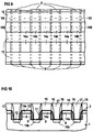
- FIG. 9 shows a top view of the sections shown in FIGS. 7 and 8.
- the position of the doped polysilicon spacers 9 was entered into this supervision as dashed lines.
- the first word lines 13 and the doped polysilicon spacers 9, which form the second word lines, run perpendicular to one another.
- the source / drain regions 14a, 14b have dimensions of F x F parallel to the main surface 2. They are arranged directly next to each other (see Figure 9). The distance between adjacent source / drain regions 14a, 14b parallel to the trenches 5 is also F.
- Each source / drain region 14a, 14b belongs to two adjacent planar MOS transistors.
- the vertical MOS transistors are implemented in the side walls of the trenches 5 and do not require any area parallel to the main area 2. Therefore, the area requirement for two memory cells, which comprise a planar MOS transistor and a vertical MOS transistor, is 2 F 2 . The average space requirement per memory cell is therefore F 2 .
- an intermediate oxide layer 15 is produced over the entire surface (see FIG. 10).
- the intermediate oxide layer 15 is formed in a layer thickness of, for example, 1600 nm.
- Contact holes are opened in the intermediate oxide layer 15 to source / drain regions 14b located at the bottom of the trenches 5.
- the side walls of the contact holes are provided with insulating spacers 16.
- the insulating spacers 16 are formed, for example, by depositing an SiO 2 layer in a TEOS process in a layer thickness of, for example, 30 to 80 nm and anisotropic etching back of the SiO 2 layer.
- the spacers 16 may cover parts of the source / drain regions 14a or the word lines 13 located on the main surface 2 as a result of adjustment errors.
- the contact holes are finally filled with metal fillings 17.
- a metal layer is applied by sputtering or vapor deposition and structured using photolithographic process steps and an etching step.
- the metal fillings 17 are formed, for example, from aluminum or tungsten.
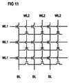
- FIG. 11 shows a circuit diagram for a memory cell array with 3 ⁇ 3 memory cell pairs.
- the individual memory cells are arranged in a NAND configuration.
- WL1 denotes the first word lines 13, which each connect gate electrodes of planar MOS transistors to one another.
- WL2 denotes the second word lines which are formed by the doped polysilicon spacers 9 and which each connect gate electrodes of vertical MOS transistors to one another.
- BL denotes the bit lines which are implemented by the planar MOS transistors which are respectively connected in series and are arranged on the main surface 2 and on the bottom of the trenches 5.
- the planar MOS transistors are evaluated via the bit lines BL and the respective first word lines WL1.
- the vertical MOS transistors are each evaluated between an adjacent bit line BL of planar MOS transistors which are arranged on the main surface 2 and the source / drain region 14b arranged at the bottom of the trench 5, which via the metal filling 17 has a reference potential is placed.
- the programming of the memory cell arrangement takes place during the production of the memory cell arrangement through the first channel implantation, the second channel implantation and the third channel implantation.
- the information stored in the process is transferred via the arrangement of the openings in the lacquer masks used in the channel implantations.
- the second channel implantation for programming the vertical MOS transistors can alternatively take place after the production of the first word lines 13.
- the second resist mask is generated above the hard mask that is used to structure the first word lines 13.
- the openings overlap the hard mask, so that the adjustment of the second paint mask parallel to the course of the trenches is not critical.
- the depletion channels in the side walls of the trenches are formed by oblique implantation of boron.
- the energy during the ion implantation is adjusted so that the boron ions pass through the doped polysilicon spacer 9 and the gate dielectric 8 into the side wall of the trenches 5.
- the implantation takes place, for example, with an energy of 50 keV.
- Different threshold voltages of the MOS transistors can also be realized during production by forming gate dielectrics of different thicknesses in the planar and / or vertical MOS transistors.
- a material with adhesion points is used as the gate dielectric 8 and as the further gate dielectric 12.
- the gate dielectric 8 and the further gate dielectric 12 are formed, for example, from a dielectric multiple layer, in which at least one layer is provided, which has an increased charge carrier capture cross section in comparison with at least one further layer in the multiple layer.
- the dielectric multilayer preferably comprises an SiO 2 layer, an Si 3 N 4 layer and an SiO 2 layer (so-called ONO).
- the layer thicknesses in the multilayer are dimensioned such that the multilayer corresponds in terms of the gate capacitance to a layer made of thermal SiO with a thickness of, for example, 10 nm.
- layer thicknesses of 4 nm each and a layer thickness of 4 nm is required for the Si 3 N 4 layer.
- the memory cell arrangement is programmed after its production by injecting charge carriers, especially electrons, into the gate dielectric 8 or the further gate dielectric 12.
- the charge carriers can be made by Fowler -Nordheim tunnels or hot electron injection.
- the first channel implantation, the second channel implantation and the third channel implantation as well as the lacquer masks used in this case are omitted.
- enhancement transistors for the planar MOS transistors and the vertical MOS transistors.
- the different threshold voltages are set to, for example, 0.5 volts and 1.5 volts.
Landscapes
- Semiconductor Memories (AREA)
Applications Claiming Priority (2)
| Application Number | Priority Date | Filing Date | Title |
|---|---|---|---|
| DE19603810A DE19603810C1 (de) | 1996-02-02 | 1996-02-02 | Speicherzellenanordnung und Verfahren zu deren Herstellung |
| DE19603810 | 1996-02-02 |
Publications (3)
| Publication Number | Publication Date |
|---|---|
| EP0788165A2 true EP0788165A2 (fr) | 1997-08-06 |
| EP0788165A3 EP0788165A3 (fr) | 1997-12-10 |
| EP0788165B1 EP0788165B1 (fr) | 2004-02-04 |
Family
ID=7784367
Family Applications (1)
| Application Number | Title | Priority Date | Filing Date |
|---|---|---|---|
| EP96119225A Expired - Lifetime EP0788165B1 (fr) | 1996-02-02 | 1996-11-29 | Système de cellules de mémoire et son procédé de fabrication |
Country Status (6)
| Country | Link |
|---|---|
| US (2) | US5821591A (fr) |
| EP (1) | EP0788165B1 (fr) |
| JP (1) | JPH09213816A (fr) |
| KR (1) | KR100400528B1 (fr) |
| DE (2) | DE19603810C1 (fr) |
| TW (1) | TW317033B (fr) |
Cited By (27)
| Publication number | Priority date | Publication date | Assignee | Title |
|---|---|---|---|---|
| US6873539B1 (en) | 2001-06-18 | 2005-03-29 | Pierre Fazan | Semiconductor device |
| US6912150B2 (en) | 2003-05-13 | 2005-06-28 | Lionel Portman | Reference current generator, and method of programming, adjusting and/or operating same |
| US6982918B2 (en) | 2002-04-18 | 2006-01-03 | Pierre Fazan | Data storage device and refreshing method for use with such device |
| US7061050B2 (en) | 2002-04-18 | 2006-06-13 | Innovative Silicon S.A. | Semiconductor device utilizing both fully and partially depleted devices |
| US7085156B2 (en) | 2003-05-13 | 2006-08-01 | Innovative Silicon S.A. | Semiconductor memory device and method of operating same |
| US7085153B2 (en) | 2003-05-13 | 2006-08-01 | Innovative Silicon S.A. | Semiconductor memory cell, array, architecture and device, and method of operating same |
| US7177175B2 (en) | 2003-09-24 | 2007-02-13 | Innovative Silicon S.A. | Low power programming technique for a floating body memory transistor, memory cell, and memory array |
| US7335934B2 (en) | 2003-07-22 | 2008-02-26 | Innovative Silicon S.A. | Integrated circuit device, and method of fabricating same |
| US8861247B2 (en) | 2009-04-27 | 2014-10-14 | Micron Technology, Inc. | Techniques for providing a direct injection semiconductor memory device |
| US8947965B2 (en) | 2009-07-27 | 2015-02-03 | Micron Technology Inc. | Techniques for providing a direct injection semiconductor memory device |
| US8964479B2 (en) | 2010-03-04 | 2015-02-24 | Micron Technology, Inc. | Techniques for sensing a semiconductor memory device |
| US8982633B2 (en) | 2009-05-22 | 2015-03-17 | Micron Technology, Inc. | Techniques for providing a direct injection semiconductor memory device |
| US9019788B2 (en) | 2008-01-24 | 2015-04-28 | Micron Technology, Inc. | Techniques for accessing memory cells |
| US9019759B2 (en) | 2010-03-15 | 2015-04-28 | Micron Technology, Inc. | Techniques for providing a semiconductor memory device |
| US9064730B2 (en) | 2009-03-04 | 2015-06-23 | Micron Technology, Inc. | Techniques for forming a contact to a buried diffusion layer in a semiconductor memory device |
| US9093311B2 (en) | 2009-03-31 | 2015-07-28 | Micron Technology, Inc. | Techniques for providing a semiconductor memory device |
| US9142264B2 (en) | 2010-05-06 | 2015-09-22 | Micron Technology, Inc. | Techniques for refreshing a semiconductor memory device |
| US9240496B2 (en) | 2009-04-30 | 2016-01-19 | Micron Technology, Inc. | Semiconductor device with floating gate and electrically floating body |
| US9257155B2 (en) | 2007-05-30 | 2016-02-09 | Micron Technology, Inc. | Integrated circuit having voltage generation circuitry for memory cell array, and method of operating and/or controlling same |
| US9263133B2 (en) | 2011-05-17 | 2016-02-16 | Micron Technology, Inc. | Techniques for providing a semiconductor memory device |
| US9276000B2 (en) | 2007-03-29 | 2016-03-01 | Micron Technology, Inc. | Manufacturing process for zero-capacitor random access memory circuits |
| US9331083B2 (en) | 2009-07-10 | 2016-05-03 | Micron Technology, Inc. | Techniques for providing a semiconductor memory device |
| US9553186B2 (en) | 2008-09-25 | 2017-01-24 | Micron Technology, Inc. | Recessed gate silicon-on-insulator floating body device with self-aligned lateral isolation |
| US9559216B2 (en) | 2011-06-06 | 2017-01-31 | Micron Technology, Inc. | Semiconductor memory device and method for biasing same |
| US9812179B2 (en) | 2009-11-24 | 2017-11-07 | Ovonyx Memory Technology, Llc | Techniques for reducing disturbance in a semiconductor memory device |
| US10304837B2 (en) | 2007-11-29 | 2019-05-28 | Ovonyx Memory Technology, Llc | Integrated circuit having memory cell array including barriers, and method of manufacturing same |
| US10418091B2 (en) | 2005-09-07 | 2019-09-17 | Ovonyx Memory Technology, Llc | Memory cell and memory cell array having an electrically floating body transistor, and methods of operating same |
Families Citing this family (61)
| Publication number | Priority date | Publication date | Assignee | Title |
|---|---|---|---|---|
| DE19732871C2 (de) * | 1997-07-30 | 1999-05-27 | Siemens Ag | Festwert-Speicherzellenanordnung, Ätzmaske für deren Programmierung und Verfahren zu deren Herstellung |
| TW406419B (en) * | 1998-01-15 | 2000-09-21 | Siemens Ag | Memory-cells arrangement and its production method |
| US6191446B1 (en) * | 1998-03-04 | 2001-02-20 | Advanced Micro Devices, Inc. | Formation and control of a vertically oriented transistor channel length |
| US6034388A (en) * | 1998-05-15 | 2000-03-07 | International Business Machines Corporation | Depleted polysilicon circuit element and method for producing the same |
| US7253047B2 (en) * | 1999-09-01 | 2007-08-07 | Micron Technology, Inc. | Semiconductor processing methods of forming transistors, semiconductor processing methods of forming dynamic random access memory circuitry, and related integrated circuitry |
| DE10039441A1 (de) * | 2000-08-11 | 2002-02-28 | Infineon Technologies Ag | Speicherzelle, Speicherzellenanordnung und Herstellungsverfahren |
| US6580124B1 (en) * | 2000-08-14 | 2003-06-17 | Matrix Semiconductor Inc. | Multigate semiconductor device with vertical channel current and method of fabrication |
| US6627924B2 (en) * | 2001-04-30 | 2003-09-30 | Ibm Corporation | Memory system capable of operating at high temperatures and method for fabricating the same |
| US6583060B2 (en) * | 2001-07-13 | 2003-06-24 | Micron Technology, Inc. | Dual depth trench isolation |
| US6952033B2 (en) * | 2002-03-20 | 2005-10-04 | Silicon Storage Technology, Inc. | Semiconductor memory array of floating gate memory cells with buried bit-line and raised source line |
| US6917069B2 (en) | 2001-10-17 | 2005-07-12 | Silicon Storage Technology, Inc. | Semiconductor memory array of floating gate memory cells with buried bit-line and vertical word line transistor |
| US6706595B2 (en) * | 2002-03-14 | 2004-03-16 | Advanced Micro Devices, Inc. | Hard mask process for memory device without bitline shorts |
| US6894231B2 (en) * | 2002-03-19 | 2005-05-17 | Broadcom Corporation | Bus twisting scheme for distributed coupling and low power |
| US6479348B1 (en) * | 2002-03-27 | 2002-11-12 | Advanced Micro Devices, Inc. | Method of making memory wordline hard mask extension |
| US7411246B2 (en) | 2002-04-01 | 2008-08-12 | Silicon Storage Technology, Inc. | Self aligned method of forming a semiconductor memory array of floating gate memory cells with buried bit-line and raised source line, and a memory array made thereby |
| US6952034B2 (en) * | 2002-04-05 | 2005-10-04 | Silicon Storage Technology, Inc. | Semiconductor memory array of floating gate memory cells with buried source line and floating gate |
| US6891220B2 (en) * | 2002-04-05 | 2005-05-10 | Silicon Storage Technology, Inc. | Method of programming electrons onto a floating gate of a non-volatile memory cell |
| US6696339B1 (en) * | 2002-08-21 | 2004-02-24 | Micron Technology, Inc. | Dual-damascene bit line structures for microelectronic devices and methods of fabricating microelectronic devices |
| DE10240893A1 (de) * | 2002-09-04 | 2004-03-18 | Infineon Technologies Ag | Verfahren zur Herstellung von SONOS-Speicherzellen, SONOS-Speicherzelle und Speicherzellenfeld |
| DE10241173A1 (de) * | 2002-09-05 | 2004-03-11 | Infineon Technologies Ag | Halbleiterspeicher mit vertikalen Speichertransistoren in einer Zellenfeldanordnung mit 1-2F2-Zellen |
| KR100885910B1 (ko) * | 2003-04-30 | 2009-02-26 | 삼성전자주식회사 | 게이트 적층물에 oha막을 구비하는 비 휘발성 반도체메모리 장치 및 그 제조방법 |
| US6906379B2 (en) * | 2003-08-28 | 2005-06-14 | Silicon Storage Technology, Inc. | Semiconductor memory array of floating gate memory cells with buried floating gate |
| KR100540478B1 (ko) * | 2004-03-22 | 2006-01-11 | 주식회사 하이닉스반도체 | 전하 트랩을 갖는 게이트유전체를 포함한 휘발성 메모리셀 트랜지스터 및 그 제조 방법 |
| US7476939B2 (en) | 2004-11-04 | 2009-01-13 | Innovative Silicon Isi Sa | Memory cell having an electrically floating body transistor and programming technique therefor |
| US7251164B2 (en) | 2004-11-10 | 2007-07-31 | Innovative Silicon S.A. | Circuitry for and method of improving statistical distribution of integrated circuits |
| US7301838B2 (en) | 2004-12-13 | 2007-11-27 | Innovative Silicon S.A. | Sense amplifier circuitry and architecture to write data into and/or read from memory cells |
| US7301803B2 (en) | 2004-12-22 | 2007-11-27 | Innovative Silicon S.A. | Bipolar reading technique for a memory cell having an electrically floating body transistor |
| US7335943B2 (en) * | 2005-05-06 | 2008-02-26 | Atmel Corporation | Ultrascalable vertical MOS transistor with planar contacts |
| TWI269363B (en) * | 2005-06-30 | 2006-12-21 | Powerchip Semiconductor Corp | Anti-punch-through semiconductor device and manufacturing method thereof |
| US7355916B2 (en) | 2005-09-19 | 2008-04-08 | Innovative Silicon S.A. | Method and circuitry to generate a reference current for reading a memory cell, and device implementing same |
| DE102005047058B4 (de) * | 2005-09-30 | 2009-09-24 | Qimonda Ag | Herstellungsverfahren für einen Graben-Transistor und entsprechender Graben-Transistor |
| US7683430B2 (en) | 2005-12-19 | 2010-03-23 | Innovative Silicon Isi Sa | Electrically floating body memory cell and array, and method of operating or controlling same |
| US7542345B2 (en) | 2006-02-16 | 2009-06-02 | Innovative Silicon Isi Sa | Multi-bit memory cell having electrically floating body transistor, and method of programming and reading same |
| US7492632B2 (en) | 2006-04-07 | 2009-02-17 | Innovative Silicon Isi Sa | Memory array having a programmable word length, and method of operating same |
| US7606098B2 (en) | 2006-04-18 | 2009-10-20 | Innovative Silicon Isi Sa | Semiconductor memory array architecture with grouped memory cells, and method of controlling same |
| KR100764439B1 (ko) * | 2006-04-25 | 2007-10-05 | 주식회사 하이닉스반도체 | 반도체 소자의 형성 방법 |
| US7933142B2 (en) | 2006-05-02 | 2011-04-26 | Micron Technology, Inc. | Semiconductor memory cell and array using punch-through to program and read same |
| US8069377B2 (en) | 2006-06-26 | 2011-11-29 | Micron Technology, Inc. | Integrated circuit having memory array including ECC and column redundancy and method of operating the same |
| US7542340B2 (en) | 2006-07-11 | 2009-06-02 | Innovative Silicon Isi Sa | Integrated circuit including memory array having a segmented bit line architecture and method of controlling and/or operating same |
| KR101406604B1 (ko) | 2007-01-26 | 2014-06-11 | 마이크론 테크놀로지, 인코포레이티드 | 게이트형 바디 영역으로부터 격리되는 소스/드레인 영역을 포함하는 플로팅-바디 dram 트랜지스터 |
| US7808038B2 (en) | 2007-03-27 | 2010-10-05 | Sandisk 3D Llc | Method of making three dimensional NAND memory |
| US7745265B2 (en) * | 2007-03-27 | 2010-06-29 | Sandisk 3D, Llc | Method of making three dimensional NAND memory |
| US7851851B2 (en) * | 2007-03-27 | 2010-12-14 | Sandisk 3D Llc | Three dimensional NAND memory |
| US7848145B2 (en) | 2007-03-27 | 2010-12-07 | Sandisk 3D Llc | Three dimensional NAND memory |
| US8085594B2 (en) | 2007-06-01 | 2011-12-27 | Micron Technology, Inc. | Reading technique for memory cell with electrically floating body transistor |
| US8194487B2 (en) | 2007-09-17 | 2012-06-05 | Micron Technology, Inc. | Refreshing data of memory cells with electrically floating body transistors |
| US8349662B2 (en) | 2007-12-11 | 2013-01-08 | Micron Technology, Inc. | Integrated circuit having memory cell array, and method of manufacturing same |
| US8014195B2 (en) | 2008-02-06 | 2011-09-06 | Micron Technology, Inc. | Single transistor memory cell |
| US8189376B2 (en) | 2008-02-08 | 2012-05-29 | Micron Technology, Inc. | Integrated circuit having memory cells including gate material having high work function, and method of manufacturing same |
| US7957206B2 (en) | 2008-04-04 | 2011-06-07 | Micron Technology, Inc. | Read circuitry for an integrated circuit having memory cells and/or a memory cell array, and method of operating same |
| US7933140B2 (en) | 2008-10-02 | 2011-04-26 | Micron Technology, Inc. | Techniques for reducing a voltage swing |
| US7924630B2 (en) | 2008-10-15 | 2011-04-12 | Micron Technology, Inc. | Techniques for simultaneously driving a plurality of source lines |
| US8223574B2 (en) | 2008-11-05 | 2012-07-17 | Micron Technology, Inc. | Techniques for block refreshing a semiconductor memory device |
| US8148768B2 (en) * | 2008-11-26 | 2012-04-03 | Silicon Storage Technology, Inc. | Non-volatile memory cell with self aligned floating and erase gates, and method of making same |
| US8213226B2 (en) | 2008-12-05 | 2012-07-03 | Micron Technology, Inc. | Vertical transistor memory cell and array |
| US8319294B2 (en) | 2009-02-18 | 2012-11-27 | Micron Technology, Inc. | Techniques for providing a source line plane |
| US8199595B2 (en) | 2009-09-04 | 2012-06-12 | Micron Technology, Inc. | Techniques for sensing a semiconductor memory device |
| US8310893B2 (en) | 2009-12-16 | 2012-11-13 | Micron Technology, Inc. | Techniques for reducing impact of array disturbs in a semiconductor memory device |
| US8416636B2 (en) | 2010-02-12 | 2013-04-09 | Micron Technology, Inc. | Techniques for controlling a semiconductor memory device |
| US8411513B2 (en) | 2010-03-04 | 2013-04-02 | Micron Technology, Inc. | Techniques for providing a semiconductor memory device having hierarchical bit lines |
| US8369177B2 (en) | 2010-03-05 | 2013-02-05 | Micron Technology, Inc. | Techniques for reading from and/or writing to a semiconductor memory device |
Citations (2)
| Publication number | Priority date | Publication date | Assignee | Title |
|---|---|---|---|---|
| US4954854A (en) | 1989-05-22 | 1990-09-04 | International Business Machines Corporation | Cross-point lightly-doped drain-source trench transistor and fabrication process therefor |
| DE4214923A1 (de) | 1991-05-31 | 1992-12-03 | Mitsubishi Electric Corp | Masken-rom-einrichtung und verfahren zu deren herstellung |
Family Cites Families (15)
| Publication number | Priority date | Publication date | Assignee | Title |
|---|---|---|---|---|
| US4914740A (en) * | 1988-03-07 | 1990-04-03 | International Business Corporation | Charge amplifying trench memory cell |
| JPH02106966A (ja) * | 1988-10-17 | 1990-04-19 | Seiko Epson Corp | 半導体記憶装置 |
| JPH03190165A (ja) * | 1989-12-20 | 1991-08-20 | Sony Corp | 読み出し専用メモリ装置及びその製造方法 |
| JPH05102436A (ja) * | 1991-10-09 | 1993-04-23 | Ricoh Co Ltd | 半導体メモリ装置とその製造方法 |
| JP3400044B2 (ja) * | 1993-11-12 | 2003-04-28 | 株式会社東芝 | 半導体メモリおよびその製造方法 |
| US5492858A (en) * | 1994-04-20 | 1996-02-20 | Digital Equipment Corporation | Shallow trench isolation process for high aspect ratio trenches |
| US5705415A (en) * | 1994-10-04 | 1998-01-06 | Motorola, Inc. | Process for forming an electrically programmable read-only memory cell |
| US5670803A (en) * | 1995-02-08 | 1997-09-23 | International Business Machines Corporation | Three-dimensional SRAM trench structure and fabrication method therefor |
| JP2692639B2 (ja) * | 1995-03-10 | 1997-12-17 | 日本電気株式会社 | 不揮発性半導体記憶装置の製造方法 |
| DE19525070C2 (de) * | 1995-07-10 | 2001-12-06 | Infineon Technologies Ag | Elektrisch schreib- und löschbare Festwertspeicherzellenanordnung und Verfahren zu deren Herstellung |
| TW326553B (en) * | 1996-01-22 | 1998-02-11 | Handotai Energy Kenkyusho Kk | Semiconductor device and method of fabricating same |
| US5763310A (en) * | 1996-10-08 | 1998-06-09 | Advanced Micro Devices, Inc. | Integrated circuit employing simultaneously formed isolation and transistor trenches |
| DE19646419C1 (de) * | 1996-11-11 | 1998-04-30 | Siemens Ag | Verfahren zur Herstellung einer elektrisch schreib- und löschbaren Festwertspeicherzellenanordnung |
| US5933717A (en) * | 1997-03-04 | 1999-08-03 | Advanced Micro Devices, Inc. | Vertical transistor interconnect structure and fabrication method thereof |
| US5858830A (en) * | 1997-06-12 | 1999-01-12 | Taiwan Semiconductor Manufacturing Company, Ltd. | Method of making dual isolation regions for logic and embedded memory devices |
-
1996
- 1996-02-02 DE DE19603810A patent/DE19603810C1/de not_active Expired - Fee Related
- 1996-11-29 DE DE59610908T patent/DE59610908D1/de not_active Expired - Lifetime
- 1996-11-29 EP EP96119225A patent/EP0788165B1/fr not_active Expired - Lifetime
- 1996-12-06 TW TW085115076A patent/TW317033B/zh active
-
1997
- 1997-01-29 JP JP9029688A patent/JPH09213816A/ja active Pending
- 1997-01-31 KR KR1019970002920A patent/KR100400528B1/ko not_active Expired - Fee Related
- 1997-02-03 US US08/794,566 patent/US5821591A/en not_active Expired - Lifetime
-
1998
- 1998-06-10 US US09/095,260 patent/US6180458B1/en not_active Expired - Fee Related
Patent Citations (2)
| Publication number | Priority date | Publication date | Assignee | Title |
|---|---|---|---|---|
| US4954854A (en) | 1989-05-22 | 1990-09-04 | International Business Machines Corporation | Cross-point lightly-doped drain-source trench transistor and fabrication process therefor |
| DE4214923A1 (de) | 1991-05-31 | 1992-12-03 | Mitsubishi Electric Corp | Masken-rom-einrichtung und verfahren zu deren herstellung |
Cited By (48)
| Publication number | Priority date | Publication date | Assignee | Title |
|---|---|---|---|---|
| US6873539B1 (en) | 2001-06-18 | 2005-03-29 | Pierre Fazan | Semiconductor device |
| US7732816B2 (en) | 2001-06-18 | 2010-06-08 | Innovative Silicon Isi Sa | Semiconductor device |
| US6925006B2 (en) | 2001-06-18 | 2005-08-02 | Innovative Silicon S.A. | Semiconductor device |
| US6930918B2 (en) | 2001-06-18 | 2005-08-16 | Innovative Silicon S.A. | Semiconductor device |
| US6934186B2 (en) | 2001-06-18 | 2005-08-23 | Innovative Silicon S.A. | Semiconductor device |
| US6937516B2 (en) | 2001-06-18 | 2005-08-30 | Innovative Silicon S.A. | Semiconductor device |
| US6969662B2 (en) | 2001-06-18 | 2005-11-29 | Pierre Fazan | Semiconductor device |
| US7541616B2 (en) | 2001-06-18 | 2009-06-02 | Innovative Silicon Isi Sa | Semiconductor device |
| US7280399B2 (en) | 2001-06-18 | 2007-10-09 | Innovative Silicon S.A. | Semiconductor device |
| US7170807B2 (en) | 2002-04-18 | 2007-01-30 | Innovative Silicon S.A. | Data storage device and refreshing method for use with such device |
| US7514748B2 (en) | 2002-04-18 | 2009-04-07 | Innovative Silicon Isi Sa | Semiconductor device |
| US7342842B2 (en) | 2002-04-18 | 2008-03-11 | Innovative Silicon, S.A. | Data storage device and refreshing method for use with such device |
| US7061050B2 (en) | 2002-04-18 | 2006-06-13 | Innovative Silicon S.A. | Semiconductor device utilizing both fully and partially depleted devices |
| US6982918B2 (en) | 2002-04-18 | 2006-01-03 | Pierre Fazan | Data storage device and refreshing method for use with such device |
| US7187581B2 (en) | 2003-05-13 | 2007-03-06 | Innovative Silicon S.A. | Semiconductor memory device and method of operating same |
| US7085153B2 (en) | 2003-05-13 | 2006-08-01 | Innovative Silicon S.A. | Semiconductor memory cell, array, architecture and device, and method of operating same |
| US7085156B2 (en) | 2003-05-13 | 2006-08-01 | Innovative Silicon S.A. | Semiconductor memory device and method of operating same |
| US6980461B2 (en) | 2003-05-13 | 2005-12-27 | Innovative Silicon S.A. | Reference current generator, and method of programming, adjusting and/or operating same |
| US6912150B2 (en) | 2003-05-13 | 2005-06-28 | Lionel Portman | Reference current generator, and method of programming, adjusting and/or operating same |
| US7335934B2 (en) | 2003-07-22 | 2008-02-26 | Innovative Silicon S.A. | Integrated circuit device, and method of fabricating same |
| US7736959B2 (en) | 2003-07-22 | 2010-06-15 | Innovative Silicon Isi Sa | Integrated circuit device, and method of fabricating same |
| US7184298B2 (en) | 2003-09-24 | 2007-02-27 | Innovative Silicon S.A. | Low power programming technique for a floating body memory transistor, memory cell, and memory array |
| US7177175B2 (en) | 2003-09-24 | 2007-02-13 | Innovative Silicon S.A. | Low power programming technique for a floating body memory transistor, memory cell, and memory array |
| US11031069B2 (en) | 2005-09-07 | 2021-06-08 | Ovonyx Memory Technology, Llc | Memory cell and memory cell array having an electrically floating body transistor, and methods of operating same |
| US10418091B2 (en) | 2005-09-07 | 2019-09-17 | Ovonyx Memory Technology, Llc | Memory cell and memory cell array having an electrically floating body transistor, and methods of operating same |
| US9276000B2 (en) | 2007-03-29 | 2016-03-01 | Micron Technology, Inc. | Manufacturing process for zero-capacitor random access memory circuits |
| US9257155B2 (en) | 2007-05-30 | 2016-02-09 | Micron Technology, Inc. | Integrated circuit having voltage generation circuitry for memory cell array, and method of operating and/or controlling same |
| US11081486B2 (en) | 2007-11-29 | 2021-08-03 | Ovonyx Memory Technology, Llc | Integrated circuit having memory cell array including barriers, and method of manufacturing same |
| US10304837B2 (en) | 2007-11-29 | 2019-05-28 | Ovonyx Memory Technology, Llc | Integrated circuit having memory cell array including barriers, and method of manufacturing same |
| US9019788B2 (en) | 2008-01-24 | 2015-04-28 | Micron Technology, Inc. | Techniques for accessing memory cells |
| US9553186B2 (en) | 2008-09-25 | 2017-01-24 | Micron Technology, Inc. | Recessed gate silicon-on-insulator floating body device with self-aligned lateral isolation |
| US9064730B2 (en) | 2009-03-04 | 2015-06-23 | Micron Technology, Inc. | Techniques for forming a contact to a buried diffusion layer in a semiconductor memory device |
| US9093311B2 (en) | 2009-03-31 | 2015-07-28 | Micron Technology, Inc. | Techniques for providing a semiconductor memory device |
| US9425190B2 (en) | 2009-04-27 | 2016-08-23 | Micron Technology, Inc. | Techniques for providing a direct injection semiconductor memory device |
| US8861247B2 (en) | 2009-04-27 | 2014-10-14 | Micron Technology, Inc. | Techniques for providing a direct injection semiconductor memory device |
| US9240496B2 (en) | 2009-04-30 | 2016-01-19 | Micron Technology, Inc. | Semiconductor device with floating gate and electrically floating body |
| US8982633B2 (en) | 2009-05-22 | 2015-03-17 | Micron Technology, Inc. | Techniques for providing a direct injection semiconductor memory device |
| US9331083B2 (en) | 2009-07-10 | 2016-05-03 | Micron Technology, Inc. | Techniques for providing a semiconductor memory device |
| US8964461B2 (en) | 2009-07-27 | 2015-02-24 | Micron Technology, Inc. | Techniques for providing a direct injection semiconductor memory device |
| US9679612B2 (en) | 2009-07-27 | 2017-06-13 | Micron Technology, Inc. | Techniques for providing a direct injection semiconductor memory device |
| US8947965B2 (en) | 2009-07-27 | 2015-02-03 | Micron Technology Inc. | Techniques for providing a direct injection semiconductor memory device |
| US9812179B2 (en) | 2009-11-24 | 2017-11-07 | Ovonyx Memory Technology, Llc | Techniques for reducing disturbance in a semiconductor memory device |
| US8964479B2 (en) | 2010-03-04 | 2015-02-24 | Micron Technology, Inc. | Techniques for sensing a semiconductor memory device |
| US9524971B2 (en) | 2010-03-15 | 2016-12-20 | Micron Technology, Inc. | Techniques for providing a semiconductor memory device |
| US9019759B2 (en) | 2010-03-15 | 2015-04-28 | Micron Technology, Inc. | Techniques for providing a semiconductor memory device |
| US9142264B2 (en) | 2010-05-06 | 2015-09-22 | Micron Technology, Inc. | Techniques for refreshing a semiconductor memory device |
| US9263133B2 (en) | 2011-05-17 | 2016-02-16 | Micron Technology, Inc. | Techniques for providing a semiconductor memory device |
| US9559216B2 (en) | 2011-06-06 | 2017-01-31 | Micron Technology, Inc. | Semiconductor memory device and method for biasing same |
Also Published As
| Publication number | Publication date |
|---|---|
| JPH09213816A (ja) | 1997-08-15 |
| DE19603810C1 (de) | 1997-08-28 |
| EP0788165B1 (fr) | 2004-02-04 |
| US5821591A (en) | 1998-10-13 |
| DE59610908D1 (de) | 2004-03-11 |
| KR970063683A (ko) | 1997-09-12 |
| TW317033B (fr) | 1997-10-01 |
| EP0788165A3 (fr) | 1997-12-10 |
| KR100400528B1 (ko) | 2003-11-14 |
| US6180458B1 (en) | 2001-01-30 |
Similar Documents
| Publication | Publication Date | Title |
|---|---|---|
| EP0788165B1 (fr) | Système de cellules de mémoire et son procédé de fabrication | |
| DE19600423C2 (de) | Elektrisch programmierbare Speicherzellenanordnung und Verfahren zu deren Herstellung | |
| DE19514834C1 (de) | Festwertspeicherzellenanordnung und Verfahren zu deren Herstellung | |
| EP0787355B1 (fr) | Procede de production d'un groupement de cellules de memoire morte a transistors mos verticaux | |
| WO1997034323A1 (fr) | Agencement de cellules memoire avec transistors mos verticaux et procede de production correspondant | |
| EP0783180A1 (fr) | Ensemble de cellules mémoire électriquement programmable et procédé de fabrication | |
| EP0784866A1 (fr) | Dispositif de cellules de memoire a valeur fixe et son procede de fabrication | |
| EP0946985B1 (fr) | Agencement de cellules de memoire et son procede de fabrication | |
| DE19525070C2 (de) | Elektrisch schreib- und löschbare Festwertspeicherzellenanordnung und Verfahren zu deren Herstellung | |
| DE69326749T2 (de) | Nichtflüchtiger Speicher mit Schutzdiode | |
| EP0815594B1 (fr) | Systeme de cellules de memoire morte et son procede de realisation | |
| DE4303059A1 (fr) | ||
| EP0021218B1 (fr) | Cellule à mémoire semiconductrice dynamique et procédé pour sa fabrication | |
| EP0896735B1 (fr) | Configuration de cellules de memoire dans laquelle des transistors mos verticaux presentent au moins trois differentes valeurs de tension de seuil en fonction de l'information memorisee, et procede permettant de la realiser | |
| EP1518277A2 (fr) | Procede pour produire un champ de cellule memoire nrom | |
| EP0864177B1 (fr) | Groupement de cellules de memoire morte et procede de fabrication correspondant | |
| DE19727436C1 (de) | DRAM-Zellenanordnung mit dynamischen selbstverstärkenden Speicherzellen und Verfahren zu deren Herstellung | |
| EP0865667B1 (fr) | Memoire morte et son procede de production | |
| DE69116022T2 (de) | Verfahren zur Herstellung eines EPROM-Speichers mit unterschiedlichen Source- und Drain-Strukturen | |
| DE19544327C2 (de) | Festwert-Speicherzellenanordnung und Verfahren zu deren Herstellung |
Legal Events
| Date | Code | Title | Description |
|---|---|---|---|
| PUAI | Public reference made under article 153(3) epc to a published international application that has entered the european phase |
Free format text: ORIGINAL CODE: 0009012 |
|
| AK | Designated contracting states |
Kind code of ref document: A2 Designated state(s): DE FR GB IT |
|
| PUAL | Search report despatched |
Free format text: ORIGINAL CODE: 0009013 |
|
| AK | Designated contracting states |
Kind code of ref document: A3 Designated state(s): DE FR GB IT |
|
| 17P | Request for examination filed |
Effective date: 19980505 |
|
| RAP1 | Party data changed (applicant data changed or rights of an application transferred) |
Owner name: INFINEON TECHNOLOGIES AG |
|
| 17Q | First examination report despatched |
Effective date: 20030102 |
|
| GRAP | Despatch of communication of intention to grant a patent |
Free format text: ORIGINAL CODE: EPIDOSNIGR1 |
|
| GRAS | Grant fee paid |
Free format text: ORIGINAL CODE: EPIDOSNIGR3 |
|
| GRAA | (expected) grant |
Free format text: ORIGINAL CODE: 0009210 |
|
| AK | Designated contracting states |
Kind code of ref document: B1 Designated state(s): DE FR GB IT |
|
| REG | Reference to a national code |
Ref country code: GB Ref legal event code: FG4D Free format text: NOT ENGLISH |
|
| REF | Corresponds to: |
Ref document number: 59610908 Country of ref document: DE Date of ref document: 20040311 Kind code of ref document: P |
|
| GBT | Gb: translation of ep patent filed (gb section 77(6)(a)/1977) |
Effective date: 20040324 |
|
| ET | Fr: translation filed | ||
| PLBE | No opposition filed within time limit |
Free format text: ORIGINAL CODE: 0009261 |
|
| STAA | Information on the status of an ep patent application or granted ep patent |
Free format text: STATUS: NO OPPOSITION FILED WITHIN TIME LIMIT |
|
| 26N | No opposition filed |
Effective date: 20041105 |
|
| PG25 | Lapsed in a contracting state [announced via postgrant information from national office to epo] |
Ref country code: IT Free format text: LAPSE BECAUSE OF NON-PAYMENT OF DUE FEES Effective date: 20051129 |
|
| PGFP | Annual fee paid to national office [announced via postgrant information from national office to epo] |
Ref country code: GB Payment date: 20101118 Year of fee payment: 15 |
|
| PGFP | Annual fee paid to national office [announced via postgrant information from national office to epo] |
Ref country code: FR Payment date: 20111130 Year of fee payment: 16 |
|
| PGFP | Annual fee paid to national office [announced via postgrant information from national office to epo] |
Ref country code: DE Payment date: 20120112 Year of fee payment: 16 |
|
| GBPC | Gb: european patent ceased through non-payment of renewal fee |
Effective date: 20121129 |
|
| REG | Reference to a national code |
Ref country code: FR Ref legal event code: ST Effective date: 20130731 |
|
| REG | Reference to a national code |
Ref country code: DE Ref legal event code: R119 Ref document number: 59610908 Country of ref document: DE Effective date: 20130601 |
|
| PG25 | Lapsed in a contracting state [announced via postgrant information from national office to epo] |
Ref country code: DE Free format text: LAPSE BECAUSE OF NON-PAYMENT OF DUE FEES Effective date: 20130601 |
|
| PG25 | Lapsed in a contracting state [announced via postgrant information from national office to epo] |
Ref country code: FR Free format text: LAPSE BECAUSE OF NON-PAYMENT OF DUE FEES Effective date: 20121130 Ref country code: GB Free format text: LAPSE BECAUSE OF NON-PAYMENT OF DUE FEES Effective date: 20121129 |