EP0789430A2 - Méthode de fabrication d'un dispositif laser à semi-conducteur - Google Patents
Méthode de fabrication d'un dispositif laser à semi-conducteur Download PDFInfo
- Publication number
- EP0789430A2 EP0789430A2 EP97106425A EP97106425A EP0789430A2 EP 0789430 A2 EP0789430 A2 EP 0789430A2 EP 97106425 A EP97106425 A EP 97106425A EP 97106425 A EP97106425 A EP 97106425A EP 0789430 A2 EP0789430 A2 EP 0789430A2
- Authority
- EP
- European Patent Office
- Prior art keywords
- bars
- semiconductor laser
- laser device
- electrodes
- layered structure
- Prior art date
- Legal status (The legal status is an assumption and is not a legal conclusion. Google has not performed a legal analysis and makes no representation as to the accuracy of the status listed.)
- Granted
Links
Images


Classifications
-
- H—ELECTRICITY
- H01—ELECTRIC ELEMENTS
- H01S—DEVICES USING THE PROCESS OF LIGHT AMPLIFICATION BY STIMULATED EMISSION OF RADIATION [LASER] TO AMPLIFY OR GENERATE LIGHT; DEVICES USING STIMULATED EMISSION OF ELECTROMAGNETIC RADIATION IN WAVE RANGES OTHER THAN OPTICAL
- H01S5/00—Semiconductor lasers
- H01S5/04—Processes or apparatus for excitation, e.g. pumping, e.g. by electron beams
- H01S5/042—Electrical excitation ; Circuits therefor
- H01S5/0425—Electrodes, e.g. characterised by the structure
- H01S5/04252—Electrodes, e.g. characterised by the structure characterised by the material
-
- H—ELECTRICITY
- H01—ELECTRIC ELEMENTS
- H01S—DEVICES USING THE PROCESS OF LIGHT AMPLIFICATION BY STIMULATED EMISSION OF RADIATION [LASER] TO AMPLIFY OR GENERATE LIGHT; DEVICES USING STIMULATED EMISSION OF ELECTROMAGNETIC RADIATION IN WAVE RANGES OTHER THAN OPTICAL
- H01S5/00—Semiconductor lasers
- H01S5/04—Processes or apparatus for excitation, e.g. pumping, e.g. by electron beams
- H01S5/042—Electrical excitation ; Circuits therefor
- H01S5/0425—Electrodes, e.g. characterised by the structure
- H01S5/04254—Electrodes, e.g. characterised by the structure characterised by the shape
-
- H—ELECTRICITY
- H01—ELECTRIC ELEMENTS
- H01S—DEVICES USING THE PROCESS OF LIGHT AMPLIFICATION BY STIMULATED EMISSION OF RADIATION [LASER] TO AMPLIFY OR GENERATE LIGHT; DEVICES USING STIMULATED EMISSION OF ELECTROMAGNETIC RADIATION IN WAVE RANGES OTHER THAN OPTICAL
- H01S5/00—Semiconductor lasers
- H01S5/10—Construction or shape of the optical resonator, e.g. extended or external cavity, coupled cavities, bent-guide, varying width, thickness or composition of the active region
- H01S5/16—Window-type lasers, i.e. with a region of non-absorbing material between the active region and the reflecting surface
- H01S5/164—Window-type lasers, i.e. with a region of non-absorbing material between the active region and the reflecting surface with window regions comprising semiconductor material with a wider bandgap than the active layer
-
- H—ELECTRICITY
- H01—ELECTRIC ELEMENTS
- H01S—DEVICES USING THE PROCESS OF LIGHT AMPLIFICATION BY STIMULATED EMISSION OF RADIATION [LASER] TO AMPLIFY OR GENERATE LIGHT; DEVICES USING STIMULATED EMISSION OF ELECTROMAGNETIC RADIATION IN WAVE RANGES OTHER THAN OPTICAL
- H01S5/00—Semiconductor lasers
- H01S5/02—Structural details or components not essential to laser action
- H01S5/0201—Separation of the wafer into individual elements, e.g. by dicing, cleaving, etching or directly during growth
-
- H—ELECTRICITY
- H01—ELECTRIC ELEMENTS
- H01S—DEVICES USING THE PROCESS OF LIGHT AMPLIFICATION BY STIMULATED EMISSION OF RADIATION [LASER] TO AMPLIFY OR GENERATE LIGHT; DEVICES USING STIMULATED EMISSION OF ELECTROMAGNETIC RADIATION IN WAVE RANGES OTHER THAN OPTICAL
- H01S5/00—Semiconductor lasers
- H01S5/02—Structural details or components not essential to laser action
- H01S5/028—Coatings ; Treatment of the laser facets, e.g. etching, passivation layers or reflecting layers
- H01S5/0281—Coatings made of semiconductor materials
-
- Y—GENERAL TAGGING OF NEW TECHNOLOGICAL DEVELOPMENTS; GENERAL TAGGING OF CROSS-SECTIONAL TECHNOLOGIES SPANNING OVER SEVERAL SECTIONS OF THE IPC; TECHNICAL SUBJECTS COVERED BY FORMER USPC CROSS-REFERENCE ART COLLECTIONS [XRACs] AND DIGESTS
- Y10—TECHNICAL SUBJECTS COVERED BY FORMER USPC
- Y10S—TECHNICAL SUBJECTS COVERED BY FORMER USPC CROSS-REFERENCE ART COLLECTIONS [XRACs] AND DIGESTS
- Y10S148/00—Metal treatment
- Y10S148/026—Deposition thru hole in mask
-
- Y—GENERAL TAGGING OF NEW TECHNOLOGICAL DEVELOPMENTS; GENERAL TAGGING OF CROSS-SECTIONAL TECHNOLOGIES SPANNING OVER SEVERAL SECTIONS OF THE IPC; TECHNICAL SUBJECTS COVERED BY FORMER USPC CROSS-REFERENCE ART COLLECTIONS [XRACs] AND DIGESTS
- Y10—TECHNICAL SUBJECTS COVERED BY FORMER USPC
- Y10S—TECHNICAL SUBJECTS COVERED BY FORMER USPC CROSS-REFERENCE ART COLLECTIONS [XRACs] AND DIGESTS
- Y10S148/00—Metal treatment
- Y10S148/095—Laser devices
-
- Y—GENERAL TAGGING OF NEW TECHNOLOGICAL DEVELOPMENTS; GENERAL TAGGING OF CROSS-SECTIONAL TECHNOLOGIES SPANNING OVER SEVERAL SECTIONS OF THE IPC; TECHNICAL SUBJECTS COVERED BY FORMER USPC CROSS-REFERENCE ART COLLECTIONS [XRACs] AND DIGESTS
- Y10—TECHNICAL SUBJECTS COVERED BY FORMER USPC
- Y10S—TECHNICAL SUBJECTS COVERED BY FORMER USPC CROSS-REFERENCE ART COLLECTIONS [XRACs] AND DIGESTS
- Y10S148/00—Metal treatment
- Y10S148/104—Mask, movable
-
- Y—GENERAL TAGGING OF NEW TECHNOLOGICAL DEVELOPMENTS; GENERAL TAGGING OF CROSS-SECTIONAL TECHNOLOGIES SPANNING OVER SEVERAL SECTIONS OF THE IPC; TECHNICAL SUBJECTS COVERED BY FORMER USPC CROSS-REFERENCE ART COLLECTIONS [XRACs] AND DIGESTS
- Y10—TECHNICAL SUBJECTS COVERED BY FORMER USPC
- Y10S—TECHNICAL SUBJECTS COVERED BY FORMER USPC CROSS-REFERENCE ART COLLECTIONS [XRACs] AND DIGESTS
- Y10S148/00—Metal treatment
- Y10S148/106—Masks, special
-
- Y—GENERAL TAGGING OF NEW TECHNOLOGICAL DEVELOPMENTS; GENERAL TAGGING OF CROSS-SECTIONAL TECHNOLOGIES SPANNING OVER SEVERAL SECTIONS OF THE IPC; TECHNICAL SUBJECTS COVERED BY FORMER USPC CROSS-REFERENCE ART COLLECTIONS [XRACs] AND DIGESTS
- Y10—TECHNICAL SUBJECTS COVERED BY FORMER USPC
- Y10S—TECHNICAL SUBJECTS COVERED BY FORMER USPC CROSS-REFERENCE ART COLLECTIONS [XRACs] AND DIGESTS
- Y10S148/00—Metal treatment
- Y10S148/143—Shadow masking
-
- Y—GENERAL TAGGING OF NEW TECHNOLOGICAL DEVELOPMENTS; GENERAL TAGGING OF CROSS-SECTIONAL TECHNOLOGIES SPANNING OVER SEVERAL SECTIONS OF THE IPC; TECHNICAL SUBJECTS COVERED BY FORMER USPC CROSS-REFERENCE ART COLLECTIONS [XRACs] AND DIGESTS
- Y10—TECHNICAL SUBJECTS COVERED BY FORMER USPC
- Y10S—TECHNICAL SUBJECTS COVERED BY FORMER USPC CROSS-REFERENCE ART COLLECTIONS [XRACs] AND DIGESTS
- Y10S438/00—Semiconductor device manufacturing: process
- Y10S438/942—Masking
- Y10S438/945—Special, e.g. metal
Definitions
- semiconductor laser devices having such advantages as small size, high efficiency, low cost, etc. have been put to practical uses, and thereby applied to general industrial and consumer appliances in which a laser beam source had been difficult to use in the past.
- the semiconductor laser devices having these advantages are expected to be used for the formation of high-speed optical disks, the effective generation of second harmonics and solid-state laser beams, the formation of high-speed laser printers, the extension of a relay distance and the formation of high-speed transmission in optical communication systems using optical fiber amplifiers, the formation of remarkably compact laser beam machines and laser treatment machines by making it possible to operate the semiconductor laser devices having these advantages at a high output power level.
- FIG. 12a An example of growing window layers on light-emitting end facets by the above-mentioned MOCVD method is shown in Figure 12a .
- a wafer with an internal structure (layered structure) including an active region is cleaved to form a bar 2 in which the front and back end facets are exposed.
- the bar 2 is inserted into a slot in a holder 905 so that a reverse surface (substrate side) is faced down, and placed in an MOCVD device.
- AlGaAs high resistance layers 930A , 930B , and 930C are formed on the front end facet, the back end facet, and a top surface of the layered structure, respectively.
- the bars 2 are taken out of the holder 901 and heated in a heat treatment furnace at 450°C for 10 minutes.
- the bars 2 are inserted into the holder 901 so that each top surface of the layered structure is faced up and the mask 902 is fixed.
- the resulting holder 901 is placed in the vacuum vapor deposition machine, and Mo/Au electrodes are formed on the AuGe/Ni electrodes by vacuum deposition.
- the bars 2 placed in the holder 901 are inverted, and then Al electrodes are formed on the AuZn electrodes by vacuum deposition. In this way, the electrodes are formed on the top surface of the layered structure and the reverse surfaces of the bars, other than the end facets thereof.
- the unwanted growth layer is removed by an etching technique according to the method of this invention, there is an advantage that the resulting window layer has a uniform thickness while the conventional method for controlling the growth of the unwanted growth layer by covering the surface of the semiconductor laser device provides a window layer with uneven thickness.
- Figure 8 is a cross-sectional view of a semiconductor laser device produced in accordance with Examples 1 and 5.
- Al 0.5 Ga 0.5 As high resistance layers 30A , 30B , and 30C (unwanted growth layer), each having a thickness of 0.3 ⁇ m are grown on a front end facet, a back end facet, and the top surface of the layered structure of each bar, respectively as shown in Figure 1b by the MOCVD method. At this time, the bars are placed so that each reverse surface is faced up, and the As 0.5 Ga 0.5 As high resistance layer 30C can be grown on the respective reverse surfaces of the bars.
- the mask set is placed in a vacuum deposition machine so that the mask 91 is on the underside, and under this condition, AuGe/Ni electrodes 40 are formed on the top surfaces of the layered structure of the bars 2 by vacuum deposition as shown in Figure 8 .
- the mask set is inverted, and under this condition, AuZn electrodes 42 are formed on the reverse surfaces of the bars 2 by vacuum deposition.
- the mask set having the bars 2 is put in a furnace and heated at 450°C for 10 minutes.
- the mask set is placed so that the mask 91 is on the underside, and under this condition, Mo/Au electrodes 44 are formed on the AuGe/Ni electrodes 40 by vacuum deposition.
- the mask set is inverted and Al electrodes 46 are formed on the AuZn electrodes by vacuum deposition.
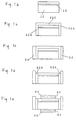
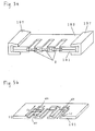
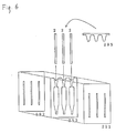
- the bars 2 thus obtained are inserted between masks 191 and 192 as shown in Figure 5a .
- the mask 191 has openings whose inside (i.e., sides in which the bars 2 are inserted) is larger than the outside thereof as shown in Figure 5b .
- the mask 192 also has the same structure as that of the mask 191 . Because of this structure, the masks 191 and 192 can firmly support the bars 2 .
- a step for forming electrodes of the present invention is applied to the production of a long wavelength type laser device having an InP substrate which is similar to that in Example 3.
- electrodes are formed by using an apparatus as shown in Figure 6 .
- the bars 2 so obtained are divided into chips and packaged.
- the bars are raised up so that each front end facet is faced down.
- the bars are placed in contact with each other, and under this condition, an Si 3 N 4 anti-reflection film is formed on each front end facet by the CVD method.
- the bars are inverted, and placed in contact with each other; under this condition, an Si 3 N 4 /Si/Si 3 N 4 /Si 3 N 4 reflection film is formed on each back end facet by the CVD method.
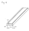
- AuZn electrodes 341 are formed on the top surfaces of the layered structure of the bars 2 .
- the apparatus is inverted and AuGe/Ni electrodes 343 are formed on the reverse surfaces of the bars 2 .
- the apparatus including the bars 2 is subjected to heat treatment at 450°C for 10 minutes. After that, the bars 2 are taken out of the apparatus and divided into chips, followed by being packaged.
- the method for forming the electrodes in the present example even bars with different widths can be produced by using the same apparatus.
- the size of a region where the electrodes are not formed can be almost exactly determined by a difference L between the tip end of the projection C and the tip ends of the projections A and C .
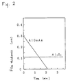
- L is 10 ⁇ m, so that a region with a size of 10 ⁇ m where the electrodes are not formed is provided in the vicinity of each end facet of the bars 2 . Even though such a region where the electrodes are not formed exists, resistance and current-optical output characteristics in semiconductor laser devices are almost the same as those of semiconductor laser devices without regions where the electrodes are not formed.
- This semiconductor laser device oscillates at a wavelength of 0.98 ⁇ m, so that it is suitable for a light source for the oscillation of an Er-doped fiber. Moreover, a semiconductor laser device with a wavelength in the range of 0.9 to 1.1 ⁇ m can be produced by varying a crystal composition ratio and thickness of the InGaAs layer 316 .
- the semiconductor laser device in the present example has a threshold current of 30 mA and a maximum output of 120 mW.
- semiconductor laser devices can be produced in a simplified method with a reduced number of steps by forming the electrodes in the similar step to those in Examples 5 to 8. Moreover, in Examples 5 to 8, the quality of semiconductor laser devices can remarkably be improved by using a method for removing the unwanted growth layer as shown in Examples 1 to 4.
- an unwanted growth layer which is formed in the production of a high output semiconductor laser device with window layers on light-emitting end facets thereof can be removed without increasing the number of steps according to the method of the present invention. Since the unwanted growth layer is removed by an etching technique, it is not required to cover the internal structure growth surface and the reverse surface. Thus, the resulting window layer has a uniform thickness.
Landscapes
- Physics & Mathematics (AREA)
- Condensed Matter Physics & Semiconductors (AREA)
- General Physics & Mathematics (AREA)
- Electromagnetism (AREA)
- Optics & Photonics (AREA)
- Semiconductor Lasers (AREA)
Applications Claiming Priority (7)
| Application Number | Priority Date | Filing Date | Title |
|---|---|---|---|
| JP46975/92 | 1992-03-04 | ||
| JP4697692 | 1992-03-04 | ||
| JP4697592 | 1992-03-04 | ||
| JP46976/92 | 1992-03-04 | ||
| JP4697692A JP2849501B2 (ja) | 1992-03-04 | 1992-03-04 | 半導体レーザの製造方法 |
| JP4046975A JP2849500B2 (ja) | 1992-03-04 | 1992-03-04 | 半導体レーザの製造方法 |
| EP92311823A EP0558856B1 (fr) | 1992-03-04 | 1992-12-24 | Méthode de fabrication d'un dispositif à laser à semi-conducteur |
Related Parent Applications (2)
| Application Number | Title | Priority Date | Filing Date |
|---|---|---|---|
| EP92311823A Division EP0558856B1 (fr) | 1992-03-04 | 1992-12-24 | Méthode de fabrication d'un dispositif à laser à semi-conducteur |
| EP92311823.6 Division | 1992-12-24 |
Publications (3)
| Publication Number | Publication Date |
|---|---|
| EP0789430A2 true EP0789430A2 (fr) | 1997-08-13 |
| EP0789430A3 EP0789430A3 (fr) | 1997-11-05 |
| EP0789430B1 EP0789430B1 (fr) | 2000-02-16 |
Family
ID=26387151
Family Applications (2)
| Application Number | Title | Priority Date | Filing Date |
|---|---|---|---|
| EP92311823A Expired - Lifetime EP0558856B1 (fr) | 1992-03-04 | 1992-12-24 | Méthode de fabrication d'un dispositif à laser à semi-conducteur |
| EP97106425A Expired - Lifetime EP0789430B1 (fr) | 1992-03-04 | 1992-12-24 | Méthode de fabrication d'un dispositif laser à semi-conducteur |
Family Applications Before (1)
| Application Number | Title | Priority Date | Filing Date |
|---|---|---|---|
| EP92311823A Expired - Lifetime EP0558856B1 (fr) | 1992-03-04 | 1992-12-24 | Méthode de fabrication d'un dispositif à laser à semi-conducteur |
Country Status (3)
| Country | Link |
|---|---|
| US (2) | US5413956A (fr) |
| EP (2) | EP0558856B1 (fr) |
| DE (2) | DE69230694T2 (fr) |
Families Citing this family (15)
| Publication number | Priority date | Publication date | Assignee | Title |
|---|---|---|---|---|
| KR0141057B1 (ko) * | 1994-11-19 | 1998-07-15 | 이헌조 | 반도체 레이저 제조방법 |
| JPH0983061A (ja) * | 1995-09-08 | 1997-03-28 | Sharp Corp | 半導体レーザ素子の製造方法および半導体レーザ素子製造装置 |
| DE19536434C2 (de) * | 1995-09-29 | 2001-11-15 | Siemens Ag | Verfahren zum Herstellen eines Halbleiterlaser-Bauelements |
| US5898721A (en) * | 1997-02-14 | 1999-04-27 | Opto Power Corporation | InGaAsP/AlGaAs/GaAs hetero structure diode laser containing indium |
| KR100767658B1 (ko) * | 2000-05-04 | 2007-10-17 | 엘지전자 주식회사 | 질화물 발광소자 제조 방법 |
| US6451120B1 (en) * | 2000-09-21 | 2002-09-17 | Adc Telecommunications, Inc. | Apparatus and method for batch processing semiconductor substrates in making semiconductor lasers |
| DE10048475C2 (de) * | 2000-09-29 | 2003-04-17 | Lumics Gmbh | Passivierung der Resonatorendflächen von Halbleiterlasern auf der Basis von III-V-Halbleitermaterial |
| GB0206482D0 (en) * | 2002-03-19 | 2002-05-01 | Denselight Semiconductors Pte | Method and apparatus for optical in wafer fabrication reactors |
| TWI697133B (zh) * | 2010-02-09 | 2020-06-21 | 晶元光電股份有限公司 | 光電元件 |
| US10205059B2 (en) | 2010-02-09 | 2019-02-12 | Epistar Corporation | Optoelectronic device and the manufacturing method thereof |
| US9640728B2 (en) | 2010-02-09 | 2017-05-02 | Epistar Corporation | Optoelectronic device and the manufacturing method thereof |
| US8483248B2 (en) * | 2010-09-14 | 2013-07-09 | Raytheon Company | Laser crystal components joined with thermal management devices |
| GB201121300D0 (en) | 2011-12-12 | 2012-01-25 | Glaxo Group Ltd | Novel composition |
| US10991547B2 (en) | 2019-09-25 | 2021-04-27 | Applied Materials, Inc. | Method and device for a carrier proximity mask |
| US10957512B1 (en) * | 2019-09-25 | 2021-03-23 | Applied Materials, Inc. | Method and device for a carrier proximity mask |
Family Cites Families (15)
| Publication number | Priority date | Publication date | Assignee | Title |
|---|---|---|---|---|
| JPS5274292A (en) * | 1975-12-17 | 1977-06-22 | Hitachi Ltd | Semiconductor laser element |
| JPS5527474A (en) * | 1978-08-19 | 1980-02-27 | Arata Kogyosho:Kk | Manufacture of spherical head for use of oiler or the like of diesel engine |
| US4230997A (en) * | 1979-01-29 | 1980-10-28 | Bell Telephone Laboratories, Incorporated | Buried double heterostructure laser device |
| US4563368A (en) * | 1983-02-14 | 1986-01-07 | Xerox Corporation | Passivation for surfaces and interfaces of semiconductor laser facets or the like |
| JPS59231885A (ja) * | 1983-06-14 | 1984-12-26 | Hitachi Ltd | 光半導体装置 |
| JPS6085586A (ja) * | 1983-10-17 | 1985-05-15 | Sony Corp | 半導体レ−ザ−の製法 |
| US4839308A (en) * | 1986-07-21 | 1989-06-13 | Gte Laboratories Incorporated | Method of making an external-coupled-cavity diode laser |
| NL8700904A (nl) * | 1987-04-16 | 1988-11-16 | Philips Nv | Halfgeleiderlaserinrichting en werkwijze voor het vervaardigen daarvan. |
| JPS6433987A (en) * | 1987-07-29 | 1989-02-03 | Nec Corp | Semiconductor laser device |
| JPH02123782A (ja) * | 1988-11-02 | 1990-05-11 | Matsushita Electric Ind Co Ltd | 半導体レーザ装置の製造方法 |
| US4910166A (en) * | 1989-01-17 | 1990-03-20 | General Electric Company | Method for partially coating laser diode facets |
| US5026660A (en) * | 1989-09-06 | 1991-06-25 | Codenoll Technology Corporation | Methods for making photodectors |
| JPH0834337B2 (ja) * | 1990-04-02 | 1996-03-29 | シャープ株式会社 | 半導体レーザ素子の製造方法 |
| JP2680917B2 (ja) * | 1990-08-01 | 1997-11-19 | シャープ株式会社 | 半導体レーザ素子の製造方法 |
| US5228047A (en) * | 1990-09-21 | 1993-07-13 | Sharp Kabushiki Kaisha | Semiconductor laser device and a method for producing the same |
-
1992
- 1992-12-22 US US07/995,064 patent/US5413956A/en not_active Expired - Lifetime
- 1992-12-24 DE DE69230694T patent/DE69230694T2/de not_active Expired - Fee Related
- 1992-12-24 EP EP92311823A patent/EP0558856B1/fr not_active Expired - Lifetime
- 1992-12-24 EP EP97106425A patent/EP0789430B1/fr not_active Expired - Lifetime
- 1992-12-24 DE DE69224617T patent/DE69224617T2/de not_active Expired - Fee Related
-
1994
- 1994-09-28 US US08/314,585 patent/US5571750A/en not_active Expired - Fee Related
Also Published As
| Publication number | Publication date |
|---|---|
| EP0558856B1 (fr) | 1998-03-04 |
| EP0789430B1 (fr) | 2000-02-16 |
| US5571750A (en) | 1996-11-05 |
| DE69230694T2 (de) | 2000-07-06 |
| US5413956A (en) | 1995-05-09 |
| EP0558856A2 (fr) | 1993-09-08 |
| DE69224617T2 (de) | 1998-09-10 |
| EP0558856A3 (en) | 1993-12-29 |
| DE69224617D1 (de) | 1998-04-09 |
| EP0789430A3 (fr) | 1997-11-05 |
| DE69230694D1 (de) | 2000-03-23 |
Similar Documents
| Publication | Publication Date | Title |
|---|---|---|
| US6990133B2 (en) | Laser diode and manufacturing method thereof | |
| EP1437809B1 (fr) | Laser à semi-conducteur composé | |
| US5413956A (en) | Method for producing a semiconductor laser device | |
| EP1583187B1 (fr) | Laser à semi-conducteur avec région sans injection de courant à proximité d'une face de résonateur | |
| JP2003258382A (ja) | GaN系レーザ素子 | |
| JP2849500B2 (ja) | 半導体レーザの製造方法 | |
| JP2000196188A (ja) | 半導体レ―ザ素子およびその製造方法 | |
| US6567444B2 (en) | High-power semiconductor laser device in which near-edge portions of active layer are removed | |
| JPH11506273A (ja) | 最高30%のアルミニウムを含む半導体材料又はアルミニウムを含まない半導体材料から成る個別の閉じ込め層を有する放射放出半導体ダイオード | |
| JP2001068789A (ja) | 半導体レーザ | |
| JP3699851B2 (ja) | 半導体発光素子の製造方法 | |
| JP3699842B2 (ja) | 化合物半導体発光素子 | |
| JP4249920B2 (ja) | 端面窓型半導体レーザ装置およびその製造方法 | |
| JP2849501B2 (ja) | 半導体レーザの製造方法 | |
| JP3257662B2 (ja) | 半導体レーザ端面のパッシベーション方法及び治具 | |
| JPH10223978A (ja) | 半導体レーザおよびその製造方法 | |
| JP3410959B2 (ja) | 半導体レーザ装置及びその製造方法 | |
| JP3564918B2 (ja) | 半導体レーザおよびその製造方法 | |
| JP3095582B2 (ja) | 半導体レーザ素子の製造方法 | |
| JPH11121876A (ja) | 半導体発光素子の製造方法 | |
| JP3754822B2 (ja) | 化合物半導体発光素子 | |
| JP2001257423A (ja) | 半導体レーザ | |
| JP2000058960A (ja) | 半導体発光素子及びその製造方法 | |
| JP3699841B2 (ja) | 化合物半導体発光素子 | |
| JPH10223979A (ja) | 半導体レーザ |
Legal Events
| Date | Code | Title | Description |
|---|---|---|---|
| PUAI | Public reference made under article 153(3) epc to a published international application that has entered the european phase |
Free format text: ORIGINAL CODE: 0009012 |
|
| 17P | Request for examination filed |
Effective date: 19970424 |
|
| AC | Divisional application: reference to earlier application |
Ref document number: 558856 Country of ref document: EP |
|
| AK | Designated contracting states |
Kind code of ref document: A2 Designated state(s): DE FR GB |
|
| PUAL | Search report despatched |
Free format text: ORIGINAL CODE: 0009013 |
|
| RIN1 | Information on inventor provided before grant (corrected) |
Inventor name: MATSUMOTO, MITSUHIRO Inventor name: YAMAMOTO, OSAMU Inventor name: SASAKI, KAZUAKI Inventor name: OHBAYASHI, KEN Inventor name: WATANABE,MASANORI |
|
| AK | Designated contracting states |
Kind code of ref document: A3 Designated state(s): DE FR GB |
|
| GRAG | Despatch of communication of intention to grant |
Free format text: ORIGINAL CODE: EPIDOS AGRA |
|
| 17Q | First examination report despatched |
Effective date: 19990407 |
|
| GRAG | Despatch of communication of intention to grant |
Free format text: ORIGINAL CODE: EPIDOS AGRA |
|
| GRAH | Despatch of communication of intention to grant a patent |
Free format text: ORIGINAL CODE: EPIDOS IGRA |
|
| GRAH | Despatch of communication of intention to grant a patent |
Free format text: ORIGINAL CODE: EPIDOS IGRA |
|
| GRAH | Despatch of communication of intention to grant a patent |
Free format text: ORIGINAL CODE: EPIDOS IGRA |
|
| GRAA | (expected) grant |
Free format text: ORIGINAL CODE: 0009210 |
|
| RIC1 | Information provided on ipc code assigned before grant |
Free format text: 7H 01S 5/02 A, 7H 01S 5/10 B |
|
| AC | Divisional application: reference to earlier application |
Ref document number: 558856 Country of ref document: EP |
|
| AK | Designated contracting states |
Kind code of ref document: B1 Designated state(s): DE FR GB |
|
| REF | Corresponds to: |
Ref document number: 69230694 Country of ref document: DE Date of ref document: 20000323 |
|
| ET | Fr: translation filed | ||
| PLBE | No opposition filed within time limit |
Free format text: ORIGINAL CODE: 0009261 |
|
| STAA | Information on the status of an ep patent application or granted ep patent |
Free format text: STATUS: NO OPPOSITION FILED WITHIN TIME LIMIT |
|
| 26N | No opposition filed | ||
| REG | Reference to a national code |
Ref country code: GB Ref legal event code: IF02 |
|
| PGFP | Annual fee paid to national office [announced via postgrant information from national office to epo] |
Ref country code: FR Payment date: 20061208 Year of fee payment: 15 |
|
| PGFP | Annual fee paid to national office [announced via postgrant information from national office to epo] |
Ref country code: GB Payment date: 20061220 Year of fee payment: 15 |
|
| PGFP | Annual fee paid to national office [announced via postgrant information from national office to epo] |
Ref country code: DE Payment date: 20061221 Year of fee payment: 15 |
|
| GBPC | Gb: european patent ceased through non-payment of renewal fee |
Effective date: 20071224 |
|
| PG25 | Lapsed in a contracting state [announced via postgrant information from national office to epo] |
Ref country code: DE Free format text: LAPSE BECAUSE OF NON-PAYMENT OF DUE FEES Effective date: 20080701 |
|
| REG | Reference to a national code |
Ref country code: FR Ref legal event code: ST Effective date: 20081020 |
|
| PG25 | Lapsed in a contracting state [announced via postgrant information from national office to epo] |
Ref country code: GB Free format text: LAPSE BECAUSE OF NON-PAYMENT OF DUE FEES Effective date: 20071224 |
|
| PG25 | Lapsed in a contracting state [announced via postgrant information from national office to epo] |
Ref country code: FR Free format text: LAPSE BECAUSE OF NON-PAYMENT OF DUE FEES Effective date: 20071231 |