EP0790659B1 - Dielektrisches Filter - Google Patents
Dielektrisches Filter Download PDFInfo
- Publication number
- EP0790659B1 EP0790659B1 EP97102363A EP97102363A EP0790659B1 EP 0790659 B1 EP0790659 B1 EP 0790659B1 EP 97102363 A EP97102363 A EP 97102363A EP 97102363 A EP97102363 A EP 97102363A EP 0790659 B1 EP0790659 B1 EP 0790659B1
- Authority
- EP
- European Patent Office
- Prior art keywords
- slot
- dielectric block
- conductor
- dielectric
- input
- Prior art date
- Legal status (The legal status is an assumption and is not a legal conclusion. Google has not performed a legal analysis and makes no representation as to the accuracy of the status listed.)
- Expired - Lifetime
Links
- 239000004020 conductor Substances 0.000 claims description 93
- 238000000034 method Methods 0.000 claims description 28
- 238000005520 cutting process Methods 0.000 claims description 24
- 238000004519 manufacturing process Methods 0.000 claims description 13
- 239000007772 electrode material Substances 0.000 claims description 3
- 238000007772 electroless plating Methods 0.000 claims description 3
- 238000002347 injection Methods 0.000 claims description 3
- 239000007924 injection Substances 0.000 claims description 3
- 238000005488 sandblasting Methods 0.000 claims description 3
- 230000008878 coupling Effects 0.000 description 15
- 238000010168 coupling process Methods 0.000 description 15
- 238000005859 coupling reaction Methods 0.000 description 15
- 238000002955 isolation Methods 0.000 description 9
- 238000012545 processing Methods 0.000 description 8
- 230000000694 effects Effects 0.000 description 5
- 230000005672 electromagnetic field Effects 0.000 description 5
- 238000000465 moulding Methods 0.000 description 4
- 238000007796 conventional method Methods 0.000 description 3
- 238000010304 firing Methods 0.000 description 3
- 238000003780 insertion Methods 0.000 description 3
- 230000037431 insertion Effects 0.000 description 3
- 229910052751 metal Inorganic materials 0.000 description 3
- 239000002184 metal Substances 0.000 description 3
- BQCADISMDOOEFD-UHFFFAOYSA-N Silver Chemical compound [Ag] BQCADISMDOOEFD-UHFFFAOYSA-N 0.000 description 2
- 230000015572 biosynthetic process Effects 0.000 description 2
- 239000007788 liquid Substances 0.000 description 2
- 230000002093 peripheral effect Effects 0.000 description 2
- 229910052709 silver Inorganic materials 0.000 description 2
- 239000004332 silver Substances 0.000 description 2
- 239000000758 substrate Substances 0.000 description 2
- BTFMCMVEUCGQDX-UHFFFAOYSA-N 1-[10-[3-[4-(2-hydroxyethyl)-1-piperidinyl]propyl]-2-phenothiazinyl]ethanone Chemical compound C12=CC(C(=O)C)=CC=C2SC2=CC=CC=C2N1CCCN1CCC(CCO)CC1 BTFMCMVEUCGQDX-UHFFFAOYSA-N 0.000 description 1
- RYGMFSIKBFXOCR-UHFFFAOYSA-N Copper Chemical compound [Cu] RYGMFSIKBFXOCR-UHFFFAOYSA-N 0.000 description 1
- 239000003082 abrasive agent Substances 0.000 description 1
- 230000005540 biological transmission Effects 0.000 description 1
- 238000004891 communication Methods 0.000 description 1
- 229910052802 copper Inorganic materials 0.000 description 1
- 239000010949 copper Substances 0.000 description 1
- 239000003989 dielectric material Substances 0.000 description 1
- 238000007598 dipping method Methods 0.000 description 1
- 239000011344 liquid material Substances 0.000 description 1
- 239000000463 material Substances 0.000 description 1
- 229960004265 piperacetazine Drugs 0.000 description 1
- 238000007747 plating Methods 0.000 description 1
- 239000000843 powder Substances 0.000 description 1
- 238000003825 pressing Methods 0.000 description 1
Images


Classifications
-
- H—ELECTRICITY
- H01—ELECTRIC ELEMENTS
- H01P—WAVEGUIDES; RESONATORS, LINES, OR OTHER DEVICES OF THE WAVEGUIDE TYPE
- H01P1/00—Auxiliary devices
- H01P1/20—Frequency-selective devices, e.g. filters
- H01P1/201—Filters for transverse electromagnetic waves
- H01P1/205—Comb or interdigital filters; Cascaded coaxial cavities
- H01P1/2056—Comb filters or interdigital filters with metallised resonator holes in a dielectric block
Definitions
- the present invention relates to a dielectric filter, and more particularly to a dielectric filter for use as an RF filter in a mobile telephone or other radio communication device or for use as an antenna duplexer.
- Fig. 6 illustrates the structure of a conventional dielectric filter using a dielectric block.
- areas filled with dots represent such areas where the bare surface of the dielectric block is exposed to the outside (without having a conductor coated thereon).
- resonance holes 2, 2 extending through a rectangular dielectric block 1 from its one end face to the opposite end face wherein the inner surface of each resonance hole is covered with an inner conductor 3 serving as a resonance conductor.
- the outer surface of the dielectric block 1 is almost entirely covered with an outer conductor 4 serving as a ground conductor.
- Input/output electrodes 5, 5 are disposed at predetermined locations on the outer conductor 4.
- the input/output electrodes 5, 5 extend to side faces from those areas formed on the bottom surface serving as an attachment surface for mounting. (The dielectric block 1 is placed such that the bottom surface is up in Fig. 6.)
- These input/output electrodes 5, 5 are electrically isolated from the output conductor 4 by outer-conductor-free areas 5a.
- An inner-conductor-free area 3a is formed near one opening end of each resonance hole 2 so that each inner conductor 3 is isolated from the outer conductor 4 by the inner-conductor-free area 3a. At the opposite opening end of each resonance hole 2, the inner conductor 3 is electrically connected to the outer conductor 4.
- the inner-conductor-free area 3a causes the corresponding end of each resonance hole 2 to act as an electrically open end.
- the inner-conductor-free area 3a may be formed by removing the inner conductors 3 formed on the inner surfaces of the resonance holes 2 along the entire circumference with a desired width using a router or the like.
- Each resonance hole 2, 2 forms one resonator stage and thus the dielectric filter includes two resonator stages.
- External coupling capacitance is formed between each input/output electrode 5 and the corresponding inner conductor 3, and each resonator stage is coupled with the corresponding input/output electrode 5 via the external coupling capacitance.
- the external coupling also depends on capacitance which occurs between the outer conductor 4 and the input/output electrodes 5 (hereafter such capacitance will be referred to as input/output electrode-to-outer conductor capacitance).
- each resonator is formed at a location spaced inward from the geometrical end so that leakage of electromagnetic field (magnetic field) from the opening end of the resonance hole is suppressed by the shielding effect provided by the outer conductor 4 present near the opening end.
- the conventional dielectric filter has the problem that it is expensive to form the inner-conductor-free areas and it is difficult to achieve high performance.
- JP 07 288 404 A relates to a dielectric resonator comprising a prismatic molding composed of a dielectric material having an upper and a lower face, a plurality of inner peripheral electrodes formed in said prismatic molding such that said inner peripheral electrodes extend between said upper and said lower faces and a conductor covering said prismatic molding to provide a ground electrode, said dielectric resonator having at least one slit provided to partially cut off the through-holes beyond the through-holes from one side face of the molding to the other side face orthogonally to the direction of the through-holes.
- the slit is provided for forming end-to-end oriented resonators.
- the object underlying the present invention is to provide a low-cost high performance dielectric filter in which an electrically open end is formed with high accuracy.
- a dielectric filter comprising:
- dielectric filter comprising:
- the dielectric filter further comprises an input/output electrode formed using a part of said outer conductor so that said input/output electrode is capacitively coupled with a corresponding inner conductor and so that an outer-conductor-free area surrounding said input/output electrode is connected to said aperture, slot or hole.
- apertures, slots or holes are formed in the dielectric block so as to form inner conductor isolation regions serving as electrically open ends of respective resonators so that the electrically open ends are located spaced inward from the end face of the dielectric block thereby ensuring that leakage of electromagnetic field is suppressed by the shielding effect of the outer conductor on the end face.
- the apertures, slots or holes providing the electrically open ends may be formed by means of cutting or similar processing using a cutting machine such as a dicer or an ultrasonic cutting machine. Since these slots may be formed simultaneously, it is possible to reduce the number of processing steps required to form the electrically open ends and it is also possible to form the slots with desired widths at desired arbitrary locations with desired accuracy. As a result, it is possible to produce a dielectric filter having small variations in characteristics at low cost.
- the gaps formed between the input/output electrodes and the outer conductor cause a reduction in capacitance between the input/output electrodes and the outer conductor, which results in an increase in the external coupling. If the external coupling is allowed to be fixed, it is possible to reduce the areas of the input/output electrodes and the outer-conductor-free areas, which results in an improvement in Qo (unloaded Q). Thus, it is possible to produce a wide-band dielectric filter having a low insertion loss.
- Fig. 1 is a perspective view of a first embodiment of a dielectric filter according to the present invention.
- the dielectric filter has a slot 11 extending across it, in parallel to one end face of a dielectric block 1, from its one side to the opposite side.
- the slot 11 is formed from the surface used as an attachment surface on which input/output electrodes 5, 5 are also formed. Formation of the slot 11 partly removes the inner conductors 3 formed on the inner surface of the resonance holes 2 by cutting the inner conductors 3 all the way through, along the entire circumference thereof, and by partly cutting away the outer-conductor-free areas 5a, 5a surrounding the respective input/output electrodes 5, 5.
- the inner conductor isolation regions 3b, 3b are formed at locations spaced inward from the end face of the dielectric block 1 thereby forming electrically open ends of the resonators.
- the dielectric block 1 is separated by the slot 11 into two parts: a shielding part and a resonator part.
- the other parts are similar to those of the conventional dielectric filter described above with reference to Fig. 6, and thus they are not described in further detail here.
- the slot 11 may be formed for example by a cutting machine such as a dicer.
- the width of the slot 11 is determined by the blade thickness of the dicer.
- the width of the slot 11 can be adjusted to a desired value by properly selecting the thickness of the blade.
- the depth of the slot 11 is determined taking into account the mechanical strength of the shielding part formed at the location directly adjacent to the end face and also taking into account the electrical characteristics to be obtained.
- the electrically open ends of the respective resonators are formed by the slot 11 at locations spaced from the end face of the dielectric block 1. Furthermore, leakage of electromagnetic field is greatly suppressed by the shielding effect provided by the outer conductor 4 present near the end face.
- the slot 11 also serves as an air layer isolating the respective input/output electrodes 5 from the outer conductor 4. This results in a reduction in capacitance between the input/output electrodes and the outer conductor and thus results in an increase in the external coupling. As a result, it becomes possible to achieve sufficient external coupling even if the areas of the input/output electrodes 5 and the outer-conductor-free regions 5a are reduced. This allows Qo and the external coupling to be determined in a more flexible fashion. With the above arrangement, for example, it is possible to expand the passband of a PHS (Personal Handy-Phone System) filter to 240 MHz from 160 MHz which is common in filters according to conventional techniques.
- PHS Personal Handy-Phone System
- Formation of a single slot 11 may cut a plurality of inner conductors 3 simultaneously and it is also possible for a single slot 11 to be formed simultaneously for a plurality of dielectric blocks 1. This allows a great reduction in the number of processing steps required to form the inner conductor isolation regions 3b and also allows improvement in accuracy of the locations and the widths of the inner conductor isolation regions 3b.
- Fig. 2 is a perspective view of a second embodiment of a dielectric filter according to the present invention.
- the dielectric filter has a slot 12 formed at a location near and in parallel to one end face of a dielectric block 1.
- the slot 12 has a small width and has a closed bottom.
- the slot 12 is formed by partially cutting the dielectric block 1 from the attachment surface on which the input/output electrodes 5, 5 are formed such that the outer-conductor-free areas 5a, 5a surrounding the respective input/output electrodes 5, 5 are partially removed and such that the inner conductors 3, 3 are cut along the entire circumference thereof.
- the slot 12 when the slot 12 is formed by partially cutting away the dielectric block together with the inner conductors 3, 3 with a predetermined proper width, the inner conductor isolation regions 3b, 3b are formed at locations spaced inward from the end face of the dielectric block 1 thereby forming electrically open ends of the resonators.
- the slot 12 corresponding to the slot 11 of the first embodiment is formed to obtain the inner conductor isolation regions 3b, 3b.
- the slot 12 may be formed using an ultrasonic cutting machine.
- the shape of the slot 12 is determined by the shape of the tip of the ultrasonic cutting machine.
- the above arrangement allows a great reduction in leakage of electromagnetic field and also a reduction in capacitance between the input/output electrodes and the outer conductor. This allows Qo and the external coupling to be determined in a more flexible fashion.
- the slot 12 may be formed by ultrasonic cutting as opposed to the conventional technique in which the inner-conductor-free areas are formed using a router. This allows a great reduction in the number of processing steps required to form the inner conductor isolation regions 3b. Furthermore, the structure of the dielectric block 1 according to this second embodiment provides an improved mechanical strength compared with the structure according to the first embodiment.
- the slot 12 may also be formed through the dielectric block 1 such that the slot 12 extends from one main surface of the dielectric block 1 to the opposite surface.
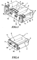
- Fig. 3 is a perspective view of a third embodiment of a dielectric filter according to the present invention.
- the dielectric filter includes two filters formed in a single dielectric block 1 wherein one filter is for reception and the other one is for transmission so that the dielectric filter can be used as an antenna duplexer.
- the dielectric filter includes four resonance holes 2 formed in the dielectric block 1 such that each resonance hole 2 extends from one end face to the opposite end face wherein the inner surface of each resonance hole 2 is covered with an inner conductor. Nearly all of the outer surface of the dielectric block 1 is covered with an outer conductor 4.
- Three input/output electrodes 5 are formed within the outer conductor 4 at proper locations on the outer surface of the dielectric block 1. The input/output electrode 5 located at the center serves as an antenna electrode which is used by both filters.
- Slots 11, 11 are formed on either side at locations near one end face of the dielectric block 1 such that the slots 11, 11 extend through the dielectric block 1 from one main surface thereof to the opposite surface.
- Slots 12, 12 each having a closed bottom are formed in the middle.
- the slots 11, 11 are formed so that the inner conductors 3, 3 of the respective resonance holes 2, 2 located near either side of the dielectric block 1 are separated into two isolated parts.
- the slots 12, 12 are formed so that the inner conductors 3, 3 of the respective resonance holes 2, 2 located in the middle of the dielectric block 1 are separated into two isolated parts.
- inner conductor isolation regions 3b, 3b, 3b, 3b are formed at locations spaced inward from the end face of the dielectric block 1.
- the respective slots 11, 12 also partially remove the outer-conductor-free areas 5a surrounding the input/output electrodes 5.
- the slots 11, 11 may be formed using a cutting machine such as a dicer.
- the slots 12, 12 may be formed using a cutting machine such as an ultrasonic cutting machine.
- a cutting machine such as an ultrasonic cutting machine.
- the slots 11, 11 may be formed using an ultrasonic cutting machine, it is more desirable to form them using a dicer or a similar cutting machine so as to reduce the number of processing steps and thus reduce the production cost.
- the slots 11 are not limited to those employed in the above embodiments.
- the slot 11 may be formed such that it extends inward from the surface opposite to the attachment surface (the lower surface) as shown in Fig. 4.
- the slots 11 are not necessarily required to extend entirely through the dielectric block from one main surface to the opposite surface, and may be formed for example as shown in Fig. 5.
- the slots 11 may be formed using an ultrasonic cutting machine.
- the shapes and locations of the slots may be determined taking into account the required mechanical strength and electrical characteristics and the specifications to be satisfied.
- each resonance hole has an uniform diameter
- the shape of each resonance hole is not limited to that.
- the resonance holes may also be formed in a so-called stepped shape having large-diameter and small-diameter portions.
- the resonance holes are formed in a stepped shape, it is possible to adjust the coupling between adjacent resonators over a wider range. This allows the dielectric filter to have better performance in an expanded variety of characteristics.
- the dielectric filter is assumed to be of a comb line coupling type in which all resonance holes have their electrically open end on the same side
- the dielectric filter may also be formed as an interdigital coupling type in which the electrically open ends are arranged alternately on either side.
- the present invention may also be applied to a dielectric filter in which both ends of resonance holes are electrically open.
- the dielectric filter has resonance holes formed in the dielectric block
- the invention may also be applied to a dielectric filter having no resonance holes but having inner conductors in the shape of plates formed in a dielectric block.
- a dielectric block may be formed by placing a plurality of dielectric substrates one on another and bonding them together, or may be formed in a laminated fashion so that a plurality of inner conductor plates acting as resonance electrodes are disposed on at least one surface of the bonded or laminated dielectric substrates.
- slots are formed in a dielectric block so as to form inner conductor isolation regions serving as electrically open ends of respective resonators so that the electrically open ends are located spaced inward from the end face of the dielectric block thereby ensuring that leakage of electromagnetic field is suppressed by the shielding effect of the outer conductor on the end face.
- the slots providing the electrically open ends may be formed by cutting or similar processing using a cutting machine such as a dicer or an ultrasonic cutting machine. Since these slots may be formed simultaneously, it is possible to reduce the number of processing steps required to form the electrically open ends and it is also possible to form the slots with desired widths at desired arbitrary locations with desired accuracy. As a result, it is possible to produce a dielectric filter having small variations in characteristics at low cost. In particular, if the slots are formed using a dicer, a great reduction in the number of processing steps can be achieved.
- the slots formed between the input/output electrodes and the outer conductor cause a reduction in capacitance between the input/output electrodes and the outer conductor, which results in an increase in the external coupling. Therefore, it is possible to reduce the areas of the input/output electrodes and the outer-conductor-free areas, which results in an improvement in Qo (unloaded Q). Thus, it is possible to produce a wide-band dielectric filter having a low insertion loss.
- Figs. 7 - 9 show three examples of processes for manufacturing a dielectric filter according to embodiments of the invention.
- a dielectric block or unit (or a plurality thereof) is first formed at step P1.
- the dielectric block may be formed by press forming or injection forming, for example, as discussed below in more detail.
- a conductive electrode is formed over the whole unit, providing the outer and inner conductors.
- the input/output electrodes are formed, for example by ultrasonic cutting or sandblasting.
- the inner-conductor-free portion is formed in the dielectric block, for example by dicing.
- the dielectric block is formed at step P1 by press forming, that is, by pressing powder material into a metal mold and then firing. Then the conductive electrode can be formed, so as to form the inner and outer electrodes, by dipping the dielectric block into a metal plating liquid, preferably carrying out an electroless plating process to apply a copper electrode material. Then at step P3, the outer electrode can be partially removed to form the input/output electrode or electrodes.
- the electrode removal step may be carried out by a process such as ultrasonic cutting in an abrasive liquid or, as another example, by a sandblasting process wherein an abrasive material is blown through an electrode pattern, quide or template.
- the inner-conductor-free portions are formed by a dicing process, wherein the desired portions are cut with a circular blade rotating at a high speed.
- the dielectric block may be formed by injection forming, that is, by hardening or conqealing a liquid material poured into a metal mold, and thereafter firing.
- the electrode especially a silver electrode material, my be formed by applying a silver paste to the inside and outside of the dielectric block and thereafter firing.
- the electrode-forming process of Fig. 9 can also be used on the press-formed dielectric block of Fig. 8, or alternatively, the above-described electroless plating process of Fig. 8 can be used on an injection-formed dielectric block formed according to Fig. 9.
- the various process steps described herein can be interchanged and combined in numerous ways that are well-known to those of ordinary skill in the art.
- the input/output electrodes are formed, for example, by one of the methods mentioned above in connection with Fig. 8.
- the inner-conductor-free portions are formed by dicing.
Landscapes
- Physics & Mathematics (AREA)
- Electromagnetism (AREA)
- Control Of Motors That Do Not Use Commutators (AREA)
Claims (24)
- Ein dielektrisches Filter, das folgende Merkmale aufweist:wobei die Eingangs-/Ausgangselektrode (5) mit einem entsprechenden der inneren Leiter (3) kapazitiv gekoppelt ist; undeinen dielektrischen Block (1), der ein Paar von Endflächen aufweist;eine Mehrzahl von inneren Leitern (3), die in dem dielektrischen Block (1) gebildet sind, derart, daß sich die inneren Leiter (3) zwischen dem Paar von Endflächen erstrecken und entsprechende Resonatoren bilden;einen äußeren Leiter (4), der auf einer äußeren Oberfläche des dielektrischen Blocks (1) gebildet ist;mindestens einen einzelnen durchgehenden Schlitz (11, 12), der durch die äußere Oberfläche des dielektrischen Blocks (1) und durch einen entsprechenden inneren Leiter (3) an einem jeweiligen Ort in der Nähe einer entsprechenden der Endflächen des dielektrischen Blocks (1) gebildet ist, so daß der entsprechende innere Leiter (3) durch den Schlitz (11; 12) in zwei Teile geteilt ist, um ein elektrisch offenes Ende des entsprechenden Resonators an dem Ort zu bilden; undeine Eingangs-/Ausgangselektrode (5), die an einem Teil der äußeren Oberfläche des dielektrischen Blocks (1) gebildet und durch einen Äußerer-Leiter-Freien Bereich (5a, 5a), der die Eingangs-/Ausgangselektrode (5) umgibt, von dem äußeren Leiter (4) isoliert ist;
wobei der Äußerer-Leiter-Freie Bereich (5a, 5a), der die Eingangs-/Ausgangselektrode (5) umgibt, teilweise durch den Schlitz (11; 12) definiert ist. - Ein dielektrisches Filter gemäß Anspruch 1, das ferner folgendes Merkmal aufweist:eine Mehrzahl von Resonanzlöchern (2), die jeweils eine mit dem inneren Leiter (3) bedeckte innere Oberfläche aufweisen, wobei die Resonanzlöcher (2) derart in dem dielektrischen Block (1) gebildet sind, daß sich die Resonanzlöcher (2) zwischen dem Paar von Endflächen erstrecken.
- Ein dielektrisches Filter gemäß Anspruch 1 oder 2, bei dem der innere Leiter (3) durch den Schlitz (11; 12) in einen ersten Teil geteilt ist, der einen entsprechenden Resonator bildet, der bei einer Resonanzfrequenz in Resonanz ist, wobei der Schlitz (11; 12) ein elektrisch offenes Ende des Resonators an dem Ort in der Nähe der entsprechenden Endfläche des dielektrischen Blocks (1) bildet und wobei der Schlitz (11; 12) einen zweiten Teil des inneren Leiters (3) bildet, der bei der Resonanzfrequenz im wesentlichen nicht in Resonanz ist.
- Ein dielektrisches Filter gemäß einem der Ansprüche 1 - 3, bei dem der Schlitz eine Luftschicht bereitstellt, die einen Bestandteil des Äußerer-Leiter-Freien Bereichs (5a, 5a) bildet.
- Ein dielektrisches Filter gemäß einem der Ansprüche 1 - 4, bei dem der dielektrische Block eine Mehrzahl von Seitenflächen aufweist, die sich zwischen dem Paar von Endflächen erstrecken, wobei der Schlitz durch lediglich eine der Seitenflächen gebildet ist.
- Ein dielektrisches Filter gemäß einem der Ansprüche 1 - 4, bei dem der dielektrische Block eine Mehrzahl von Seitenflächen aufweist, die sich zwischen dem Paar von Endflächen erstrecken, wobei der Schlitz durch ein Paar der Seitenflächen, die einander gegenüberliegen, gebildet ist.
- Ein dielektrisches Filter gemäß einem der Ansprüche 1 - 6, bei dem der dielektrische Block eine Mehrzahl von Seitenflächen aufweist, die sich zwischen dem Paar von Endflächen erstrecken, wobei die Eingangs/Ausgangselektrode (5) an einer der Seitenflächen gebildet ist und wobei der Schlitz durch lediglich die Seitenfläche gebildet ist, an der die Eingangs/Ausgangselektrode (5) gebildet ist.
- Ein dielektrisches Filter gemäß einem der Ansprüche 1 - 7, bei dem der Schlitz ferner durch einen weiteren inneren Leiter, der zu dem entsprechenden inneren Leiter (3) benachbart ist, gebildet ist.
- Ein Verfahren zum Herstellen eines dielektrischen Filters, das folgende Schritte aufweist:wobei die Eingangs-/Ausgangselektrode (5) mit einem entsprechenden der inneren Leiter (3) kapazitiv gekoppelt ist; undBilden eines dielektrischen Blocks (1), der ein Paar von Endflächen aufweist;Bilden einer Mehrzahl von inneren Leitern (3) in dem dielektrischen Block (1) derart, daß sich die inneren Leiter (3) zwischen dem Paar von Endflächen erstrecken und entsprechende Resonatoren bilden;Bilden eines äußeren Leiters (4) auf einer äußeren Oberfläche des dielektrischen Blocks (1);Bilden mindestens eines einzelnen durchgehenden Schlitzes (11; 12) durch die äußere Oberfläche des dielektrischen Blocks (1) und durch einen entsprechenden inneren Leiter (3) an einem jeweiligen Ort in der Nähe einer entsprechenden der Endflächen des dielektrischen Blocks (1), so daß der entsprechende innere Leiter (3) durch den Schlitz (11; 12) in zwei Teile geteilt ist, um ein elektrisch offenes Ende des entsprechenden Resonators an dem Ort zu bilden; undBilden einer Eingangs-/Ausgangselektrode (5) an einem Teil der äußeren Oberfläche des dielektrischen Blocks (1), die durch einen Äußerer-Leiter-Freien Bereich (5a, 5a), der die Eingangs-/Ausgangselektrode (5) umgibt, von dem äußeren Leiter (4) isoliert ist;
wobei der Äußerer-Leiter-Freie Bereich (5a, 5a), der die Eingangs-/Ausgangselektrode (5) umgibt, teilweise durch den Schlitz (11; 12) definiert ist. - Ein Verfahren zum Herstellen eines dielektrischen Filters gemäß Anspruch 9, bei dem der innere Leiter (3) durch den Schlitz (11; 12) in einen ersten Teil, der einen entsprechenden Resonator bildet, der bei einer Resonanzfrequenz in Resonanz gerät, geteilt ist, wobei der Schlitz (11; 12) ein elektrisch offenes Ende des Resonators an dem Ort in der Nähe der entsprechenden Endfläche des dielektrischen Blocks (1) bildet und der Schlitz (11; 12) einen zweiten Teil des inneren Leiters (3) bildet, der bei der Resonanzfrequenz im wesentlichen nicht in Resonanz gerät.
- Ein Verfahren gemäß Anspruch 9 oder 10, bei dem der dielektrische Block (1) durch ein Preßformen gebildet wird.
- Ein Verfahren gemäß Anspruch 9 oder 10, bei dem der dielektrische Block (1) durch ein Einspritzformen gebildet wird.
- Ein Verfahren gemäß einem der Ansprüche 9 - 12, bei dem die inneren und äußeren Leiter (3, 4) durch eine stromlose Plattierung gebildet werden.
- Ein Verfahren gemäß einem der Ansprüche 9 - 12, bei dem die inneren und äußeren Leiter (3, 4) durch eine Aufbringung von Elektrodenmaterialpaste, auf die ein Brennen folgt, gebildet werden.
- Ein Verfahren gemäß einem der Ansprüche 9 - 14, bei dem der Schlitz (11; 12) durch ein Vereinzeln gebildet wird.
- Ein Verfahren gemäß einem der Ansprüche 9 - 15, bei dem die Eingangs-/Ausgangselektrode (5) durch ein Ultraschall-Schneiden gebildet wird.
- Ein Verfahren gemäß einem der Ansprüche 9 - 15, bei dem die Eingangs-/Ausgangselektrode (5) durch ein Sandstrahlen gebildet wird.
- Ein Verfahren gemäß einem der Ansprüche 9 und 11 - 17, bei dem die inneren Leiter (3) an einer entsprechenden Mehrzahl von Resonanzlöchern (2) gebildet werden, die jeweils eine innere Oberfläche aufweisen, die mit einem entsprechenden inneren Leiter (3) bedeckt ist, wobei die Resonanzlöcher (2) in dem dielektrischen Block (1) gebildet sind, derart, daß sich die Resonanzlöcher (2) zwischen dem Paar von Endflächen erstrecken.
- Ein Verfahren zum Herstellen eines dielektrischen Filters gemäß Anspruch 18, bei dem der Schlitz angeordnet ist, um die Resonatoren, die durch die inneren Leiter gebildet sind, zu verkürzen, derart, daß die Resonatoren bei der gewünschten Resonanzfrequenz in Resonanz sind, wobei der Schlitz (11; 12) ein elektrisch offenes Ende des Resonators an dem Ort in der Nähe der entsprechenden Endfläche des dielektrischen Blocks (1) bildet und wobei der Schlitz (11; 12) ferner einen weiteren Teil des inneren Leiters (3) bildet, der bei der Resonanzfrequenz im wesentlichen nicht in Resonanz ist.
- Ein Verfahren zum Herstellen eines dielektrischen Filters gemäß einem der Ansprüche 9 - 19, bei dem der Schlitz eine Luftschicht bereitstellt, die einen Bestandteil des Äußerer-Leiter-Freien Bereichs (5a, 5a) bildet.
- Ein Verfahren zum Herstellen eines dielektrischen Filters gemäß einem der Ansprüche 9 - 20, bei dem der dielektrische Block eine Mehrzahl von Seitenflächen aufweist, die sich zwischen dem Paar von Endflächen erstrecken, wobei der Schlitz durch lediglich eine einzige der Seitenflächen gebildet ist.
- Ein Verfahren zum Herstellen eines dielektrischen Filters gemäß einem der Ansprüche 9 - 20, bei dem der dielektrische Block eine Mehrzahl von Seitenflächen aufweist, die sich zwischen dem Paar von Endflächen erstrecken, wobei der Schlitz durch ein Paar der Seitenflächen, die einander gegenüberliegen, gebildet ist.
- Ein Verfahren zum Herstellen eines dielektrischen Filters gemäß einem der Ansprüche 9 - 22, bei dem der dielektrische Block eine Mehrzahl von Seitenflächen aufweist, die sich zwischen dem Paar von Endflächen erstrecken, wobei die Eingangs-/Ausgangselektrode (5) an einer der Seitenflächen gebildet ist und wobei der Schlitz durch lediglich die Seitenfläche gebildet ist, an der die Eingangs-/Ausgangselektrode (5) gebildet ist.
- Ein Verfahren zum Herstellen eines dielektrischen Filters gemäß einem der Ansprüche 9 - 23, bei dem der Schlitz ferner durch einen weiteren inneren Leiter, der zu dem entsprechenden inneren Leiter (3) benachbart ist, gebildet ist.
Applications Claiming Priority (3)
| Application Number | Priority Date | Filing Date | Title |
|---|---|---|---|
| JP08029364A JP3125671B2 (ja) | 1996-02-16 | 1996-02-16 | 誘電体フィルタ |
| JP2936496 | 1996-02-16 | ||
| JP29364/96 | 1996-02-16 |
Publications (2)
| Publication Number | Publication Date |
|---|---|
| EP0790659A1 EP0790659A1 (de) | 1997-08-20 |
| EP0790659B1 true EP0790659B1 (de) | 2002-06-05 |
Family
ID=12274130
Family Applications (1)
| Application Number | Title | Priority Date | Filing Date |
|---|---|---|---|
| EP97102363A Expired - Lifetime EP0790659B1 (de) | 1996-02-16 | 1997-02-13 | Dielektrisches Filter |
Country Status (5)
| Country | Link |
|---|---|
| US (1) | US5841331A (de) |
| EP (1) | EP0790659B1 (de) |
| JP (1) | JP3125671B2 (de) |
| KR (1) | KR100268527B1 (de) |
| DE (1) | DE69712938D1 (de) |
Families Citing this family (4)
| Publication number | Priority date | Publication date | Assignee | Title |
|---|---|---|---|---|
| US6123589A (en) * | 1998-04-23 | 2000-09-26 | Murata Manufacturing Co., Ltd. | High-frequency connector with low intermodulation distortion |
| JP3440874B2 (ja) * | 1999-05-13 | 2003-08-25 | 株式会社村田製作所 | 誘電体フィルタおよび通信機 |
| JP2002344204A (ja) * | 2001-03-15 | 2002-11-29 | Murata Mfg Co Ltd | 誘電体フィルタ、誘電体デュプレクサおよび通信装置 |
| JP3329450B1 (ja) * | 2001-09-28 | 2002-09-30 | ティーディーケイ株式会社 | 誘電体装置 |
Family Cites Families (16)
| Publication number | Priority date | Publication date | Assignee | Title |
|---|---|---|---|---|
| JPS61121501A (ja) * | 1984-11-17 | 1986-06-09 | Tdk Corp | 誘電体共振器およびその製造方法 |
| JPH0246082Y2 (de) * | 1985-04-04 | 1990-12-05 | ||
| JPS6240802A (ja) * | 1985-08-16 | 1987-02-21 | Murata Mfg Co Ltd | 誘電体同軸共振器 |
| JPH01112801A (ja) * | 1987-10-26 | 1989-05-01 | Kokusai Electric Co Ltd | 誘電体帯域フィルタ |
| JPH026105A (ja) * | 1988-06-24 | 1990-01-10 | Sumitomo Metal Ind Ltd | プラスチック廃棄物の処理装置 |
| EP0470730B1 (de) * | 1990-08-08 | 1996-04-17 | Oki Electric Industry Co., Ltd. | Ultraschallschleifsystem für keramisches Filter und Verfahren zum Abgleich dafür |
| JPH04103201A (ja) * | 1990-08-22 | 1992-04-06 | Fuji Elelctrochem Co Ltd | 誘電体帯域阻止フィルタ |
| US5214398A (en) * | 1990-10-31 | 1993-05-25 | Ube Industries, Ltd. | Dielectric filter coupling structure having a compact terminal arrangement |
| JP2910807B2 (ja) * | 1991-10-25 | 1999-06-23 | 株式会社村田製作所 | 誘電体共振器装置、誘電体フィルタおよびそれらの製造方法 |
| JP3293200B2 (ja) * | 1992-04-03 | 2002-06-17 | 株式会社村田製作所 | 誘電体共振器 |
| EP0556573B1 (de) * | 1992-01-22 | 1998-09-23 | Murata Manufacturing Co., Ltd. | Dielektrischer Resonator und Verfahren zum Justieren seiner Charakteristik |
| JPH0685503A (ja) * | 1992-08-31 | 1994-03-25 | Sanyo Electric Co Ltd | 誘電体フィルタ |
| JPH06140805A (ja) * | 1992-10-26 | 1994-05-20 | Murata Mfg Co Ltd | 誘電体フィルタおよびその製造方法 |
| US5329687A (en) * | 1992-10-30 | 1994-07-19 | Teledyne Industries, Inc. | Method of forming a filter with integrally formed resonators |
| US5371717A (en) * | 1993-06-15 | 1994-12-06 | Hewlett-Packard Company | Microgrooves for apodization and focussing of wideband clinical ultrasonic transducers |
| JP3517939B2 (ja) * | 1994-04-18 | 2004-04-12 | 松下電器産業株式会社 | 誘電体共振器 |
-
1996
- 1996-02-16 JP JP08029364A patent/JP3125671B2/ja not_active Expired - Fee Related
-
1997
- 1997-01-24 KR KR1019970002103A patent/KR100268527B1/ko not_active Expired - Fee Related
- 1997-02-13 EP EP97102363A patent/EP0790659B1/de not_active Expired - Lifetime
- 1997-02-13 US US08/799,276 patent/US5841331A/en not_active Expired - Fee Related
- 1997-02-13 DE DE69712938T patent/DE69712938D1/de not_active Expired - Lifetime
Also Published As
| Publication number | Publication date |
|---|---|
| JP3125671B2 (ja) | 2001-01-22 |
| KR100268527B1 (ko) | 2000-10-16 |
| KR970063918A (ko) | 1997-09-12 |
| DE69712938D1 (de) | 2002-07-11 |
| EP0790659A1 (de) | 1997-08-20 |
| US5841331A (en) | 1998-11-24 |
| JPH09223904A (ja) | 1997-08-26 |
Similar Documents
| Publication | Publication Date | Title |
|---|---|---|
| US5731751A (en) | Ceramic waveguide filter with stacked resonators having capacitive metallized receptacles | |
| KR100319474B1 (ko) | 유전체 필터, 유전체 듀플렉서 및 통신기 장치 | |
| JP3852598B2 (ja) | 誘電体フィルタ及び分波器 | |
| US6351198B1 (en) | Dielectric filter, duplexer, and communication apparatus | |
| JP3582350B2 (ja) | 誘電体フィルタ、送受共用器および通信機 | |
| EP0790659B1 (de) | Dielektrisches Filter | |
| EP0917231B1 (de) | Dielektrisches Filter, dielektrischer Duplexer und Kommunikationsvorrichtung | |
| KR19980063696A (ko) | 유극형 유전체 필터 및 이를 이용한 유전체 듀플렉서 | |
| JP3801058B2 (ja) | 誘電体フィルタ | |
| JPH03124102A (ja) | 誘電体フィルタ | |
| KR101681899B1 (ko) | 유전체 필터 | |
| US6949987B2 (en) | Dielectric electronic component with attenuation adjustment electrode and method of adjusting attenuation characteristics of the same | |
| JP2001211005A (ja) | 誘電体デュプレクサとその周波数調整方法 | |
| KR20020011949A (ko) | 개량된 유전세라믹필터용 등가회로 | |
| JP3891138B2 (ja) | 誘電体共振部品 | |
| US6281763B1 (en) | Dielectric resonator, dielectric filter, dielectric duplexer, and method for manufacturing dielectric resonator | |
| US6844796B2 (en) | Dielectric filter having increased bandwidth | |
| KR100305577B1 (ko) | 유전체 듀플렉서의 제조방법 | |
| JP2000022405A (ja) | 複合フィルタ、アンテナ共用器及び通信機装置 | |
| KR101670893B1 (ko) | 유전체 필터 | |
| JP2004254005A (ja) | 誘電体電子部品及その共振周波数の調整法 | |
| JPH1197904A (ja) | 誘電体フィルタ及びその製造方法 | |
| JP2004242067A (ja) | 誘電体電子部品及その減衰量の調整方法 | |
| JPH0946108A (ja) | 誘電体共振器及び誘電体フィルタ | |
| JPH09312504A (ja) | 面実装型誘電体フィルタ |
Legal Events
| Date | Code | Title | Description |
|---|---|---|---|
| PUAI | Public reference made under article 153(3) epc to a published international application that has entered the european phase |
Free format text: ORIGINAL CODE: 0009012 |
|
| 17P | Request for examination filed |
Effective date: 19970213 |
|
| AK | Designated contracting states |
Kind code of ref document: A1 Designated state(s): DE FR GB |
|
| 17Q | First examination report despatched |
Effective date: 20000225 |
|
| GRAG | Despatch of communication of intention to grant |
Free format text: ORIGINAL CODE: EPIDOS AGRA |
|
| GRAG | Despatch of communication of intention to grant |
Free format text: ORIGINAL CODE: EPIDOS AGRA |
|
| GRAH | Despatch of communication of intention to grant a patent |
Free format text: ORIGINAL CODE: EPIDOS IGRA |
|
| GRAH | Despatch of communication of intention to grant a patent |
Free format text: ORIGINAL CODE: EPIDOS IGRA |
|
| GRAA | (expected) grant |
Free format text: ORIGINAL CODE: 0009210 |
|
| AK | Designated contracting states |
Kind code of ref document: B1 Designated state(s): DE FR GB |
|
| PG25 | Lapsed in a contracting state [announced via postgrant information from national office to epo] |
Ref country code: FR Free format text: LAPSE BECAUSE OF FAILURE TO SUBMIT A TRANSLATION OF THE DESCRIPTION OR TO PAY THE FEE WITHIN THE PRESCRIBED TIME-LIMIT Effective date: 20020605 |
|
| REG | Reference to a national code |
Ref country code: GB Ref legal event code: FG4D |
|
| REF | Corresponds to: |
Ref document number: 69712938 Country of ref document: DE Date of ref document: 20020711 |
|
| PG25 | Lapsed in a contracting state [announced via postgrant information from national office to epo] |
Ref country code: DE Free format text: LAPSE BECAUSE OF FAILURE TO SUBMIT A TRANSLATION OF THE DESCRIPTION OR TO PAY THE FEE WITHIN THE PRESCRIBED TIME-LIMIT Effective date: 20020906 |
|
| EN | Fr: translation not filed | ||
| PLBE | No opposition filed within time limit |
Free format text: ORIGINAL CODE: 0009261 |
|
| STAA | Information on the status of an ep patent application or granted ep patent |
Free format text: STATUS: NO OPPOSITION FILED WITHIN TIME LIMIT |
|
| 26N | No opposition filed |
Effective date: 20030306 |
|
| PGFP | Annual fee paid to national office [announced via postgrant information from national office to epo] |
Ref country code: GB Payment date: 20080213 Year of fee payment: 12 |
|
| GBPC | Gb: european patent ceased through non-payment of renewal fee |
Effective date: 20090213 |
|
| PG25 | Lapsed in a contracting state [announced via postgrant information from national office to epo] |
Ref country code: GB Free format text: LAPSE BECAUSE OF NON-PAYMENT OF DUE FEES Effective date: 20090213 |