EP0790665A1 - Chipantenne - Google Patents
Chipantenne Download PDFInfo
- Publication number
- EP0790665A1 EP0790665A1 EP97102143A EP97102143A EP0790665A1 EP 0790665 A1 EP0790665 A1 EP 0790665A1 EP 97102143 A EP97102143 A EP 97102143A EP 97102143 A EP97102143 A EP 97102143A EP 0790665 A1 EP0790665 A1 EP 0790665A1
- Authority
- EP
- European Patent Office
- Prior art keywords
- chip antenna
- conductor
- base
- printed circuit
- disposed
- Prior art date
- Legal status (The legal status is an assumption and is not a legal conclusion. Google has not performed a legal analysis and makes no representation as to the accuracy of the status listed.)
- Withdrawn
Links
- 239000004020 conductor Substances 0.000 claims abstract description 79
- 239000011521 glass Substances 0.000 claims abstract description 8
- 239000003822 epoxy resin Substances 0.000 claims abstract description 4
- 229920000647 polyepoxide Polymers 0.000 claims abstract description 4
- RYGMFSIKBFXOCR-UHFFFAOYSA-N Copper Chemical compound [Cu] RYGMFSIKBFXOCR-UHFFFAOYSA-N 0.000 claims abstract description 3
- 229910000881 Cu alloy Inorganic materials 0.000 claims abstract description 3
- 229910052802 copper Inorganic materials 0.000 claims abstract description 3
- 239000010949 copper Substances 0.000 claims abstract description 3
- 230000005855 radiation Effects 0.000 claims description 57
- 238000004804 winding Methods 0.000 claims description 8
- 230000008020 evaporation Effects 0.000 claims description 3
- 238000001704 evaporation Methods 0.000 claims description 3
- 238000007747 plating Methods 0.000 claims description 3
- 239000000470 constituent Substances 0.000 abstract description 3
- 230000001939 inductive effect Effects 0.000 abstract description 3
- 230000004048 modification Effects 0.000 description 7
- 238000012986 modification Methods 0.000 description 7
- 238000010295 mobile communication Methods 0.000 description 3
- 230000003247 decreasing effect Effects 0.000 description 1
- 238000010030 laminating Methods 0.000 description 1
Images



Classifications
-
- H—ELECTRICITY
- H01—ELECTRIC ELEMENTS
- H01Q—ANTENNAS, i.e. RADIO AERIALS
- H01Q1/00—Details of, or arrangements associated with, antennas
- H01Q1/36—Structural form of radiating elements, e.g. cone, spiral, umbrella; Particular materials used therewith
- H01Q1/38—Structural form of radiating elements, e.g. cone, spiral, umbrella; Particular materials used therewith formed by a conductive layer on an insulating support
-
- H—ELECTRICITY
- H01—ELECTRIC ELEMENTS
- H01Q—ANTENNAS, i.e. RADIO AERIALS
- H01Q1/00—Details of, or arrangements associated with, antennas
- H01Q1/36—Structural form of radiating elements, e.g. cone, spiral, umbrella; Particular materials used therewith
- H01Q1/362—Structural form of radiating elements, e.g. cone, spiral, umbrella; Particular materials used therewith for broadside radiating helical antennas
-
- H—ELECTRICITY
- H01—ELECTRIC ELEMENTS
- H01Q—ANTENNAS, i.e. RADIO AERIALS
- H01Q9/00—Electrically-short antennas having dimensions not more than twice the operating wavelength and consisting of conductive active radiating elements
- H01Q9/04—Resonant antennas
- H01Q9/0407—Substantially flat resonant element parallel to ground plane, e.g. patch antenna
- H01Q9/0428—Substantially flat resonant element parallel to ground plane, e.g. patch antenna radiating a circular polarised wave
- H01Q9/0435—Substantially flat resonant element parallel to ground plane, e.g. patch antenna radiating a circular polarised wave using two feed points
Definitions
- the present invention relates to a chip antenna and, more particularly, to a chip antenna for use in mobile communication equipment used for mobile communications and local area networks (LAN).
- LAN local area networks
- a conventional circularly-polarized-wave antenna 50 formed on a printed circuit board is generally structured as shown in Figs. 8A and 8B. More specifically, a radiation conductor 52 made of a square-shaped radiation conductor film, a 901 ⁇ 2 hybrid coupler 53 and two strip lines 54 and 55 are coated onto a printed circuit board 51. A non-reflective terminator 56 is mounted to one of the terminals of the 901 ⁇ 2 hybrid coupler 53, and a matching circuit 57 is inserted between the output side of the 901 ⁇ 2 hybrid coupler 53 and the strip lines 54 and 55. Further, a grounding radiation conductor film 59 is coated on the rear surface of the printed circuit board 51.
- the circularly-polarized-wave antenna 50 when a signal is input from a power feeding terminal 58, two outputs which have an equal amplitude and which are 901 ⁇ 2 out of phase are fed from the 901 ⁇ 2 hybrid coupler 53 through the matching circuit 57 to the strip lines 54 and 55. Since each of the strip lines 54 and 55 is connected to the central portion of the adjacent sides of the radiation conductor 52, electric currents excited by the strip line 54 and the strip line 55 flow intersecting at right angles on the radiation conductor 52, causing a circularly-polarized wave to be excited on the radiation conductor 52.
- a chip antenna comprising a base comprising at least one printed circuit board, at least one radiation conductor formed at least one of on the surface of and inside of the base; and at least one power feeding terminal, formed on the surface of the base, for applying a voltage to the radiation conductor.
- the radiation conductor is wound in the shape of a spiral. Further, the radiation conductor may be formed in a meandering shape having at least one corner.
- Figs. 1 and 2 show, respectively, a perspective view and an exploded, perspective view of a first embodiment of a chip antenna of the present invention.
- the chip antenna 10 comprises a radiation conductor 12 which is wound in the shape of a spiral inside a rectangular-parallelopiped base 11 along the direction of the length of the base 11.
- the base 11 comprises rectangular laminated sheet layers 13a to 13c made of printed circuit boards (specific inductive capacity: about 2 to 6) having a glass epoxy resin or glass fluororesin as their main constituents.
- Rectangular or substantially L-shaped conductive patterns 14a to 14h are formed on the surfaces of the sheet layers 13a and 13b from among the above sheet layers by printing, evaporation, pasting or plating. Further, viaholes 15 are provided at predetermined positions (one end or both ends of each of the conductive patterns 14e to 14h) on the sheet layer 13b along the direction of the thickness of the base.
- the radiation conductor 12 is formed inside the base 11, which radiation conductor has a rectangular- shaped winding cross section which is wound in the shape of a spiral along the direction of the length of the base 11.
- One end (one end of the conductive pattern 14a) of the radiation conductor 12 is extended onto the surface of the base 11, forming a power feeding section 16, and is connected to a power feeding terminal 17 formed on the surface of the base 11 in order to apply a voltage to the radiation conductor 12.
- the other end (one end of the conductive pattern 14h) of the radiation conductor 12 forms a free end 18 inside the base 11.
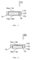
- Figs. 3 and 4 show side views of a first and a second modification of the chip antenna 10. These side views show cases when seen from the direction A in the perspective view of Fig. 1.
- the conductive patterns 14a to 14d are provided on the rear surface of the sheet layer 13a, the conductive patterns 14e to 14h are provided on the obverse surface of the sheet layer 13c, and the conductive patterns 14a to 14h are connected by the viaholes 15, thus forming a part of the radiation conductor 12 on the surface of the base 11.
- a chip antenna 10b which is a second modification of the first embodiment
- the conductive patterns 14a to 14d are provided on the rear surface of the sheet layer 13a
- the conductive patterns 14e to 14h are provided on the obverse surface of the sheet layer 13b
- the conductive patterns 14a to 14h are connected by the viaholes 15, thus forming a part of the radiation conductor 12 on the surface of the base 11.
- the conductive patterns 14a to 14h are provided on the obverse surface of the sheet layer 13a and the obverse surface of the sheet layer 13c in Fig. 2
- a similar chip antenna can be formed.
- Fig. 5 shows a perspective view of a second embodiment of a chip antenna of the present invention.
- the chip antenna 20 differs from the chip antenna 10 in that a radiation conductor 22 is wound in the shape of a spiral along the direction of the height of a base 21. Also in the chip antenna 20, a part of the radiation conductor 22 may be provided on the surface of the base 21 in the same manner as in the chip antenna 10.
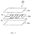
- a chip antenna 30 comprises a radiation conductor 32 formed in a meandering shape having 10 corners inside a rectangular-parallelopiped base 31.
- the base 31 comprises rectangular laminated sheet layers 33a to 33c made of printed circuit boards (specific inductive capacity: about 2 to 6) having a glass epoxy resin or glass fluororesin as their main constituents.
- a radiation conductor 32 made of copper or a copper alloy in a meandering shape is provided on the surface of the sheet layer 13b from among the above sheet layers by printing, evaporation, pasting or plating. Thereafter, the sheet layers 33a to 33c are laminated, and the radiation conductor 32 in a meandering shape is formed inside the base 31.
- the meandering-shaped base 31 is provided from one of the facing sides of the rectangular- parallelopiped base 31 to the other side.
- One end of the radiation conductor 32 is extended onto the surface of the base 31, forming a power feeding section 34, and is connected to a power feeding terminal 35 formed on the surface of the base 31 in order to apply a voltage to the base 31.
- the other end of the radiation conductor 32 forms a free end 36 inside the base 31.
- the first to third embodiments describe a case in which the base of the chip antenna is shaped like a rectangular parallelopiped, other shapes may be possible, for example, a cube, circular cylinder, pyramid, cone or sphere. Although a case utilizing one radiation conductor is described, two or more radiation conductors may be formed. In such a case, it is possible to have a plurality of resonance frequencies. Further, the position of the power feeding terminal shown in the drawings is not an indispensable condition for embodying the present invention.
- the first and second embodiments describe a case in which the entire radiation conductor or a part of the conductor is provided inside the base, the entire radiation conductor may be provided on the surface of the base.
- the shape of the winding cross section intersecting at right angles to the winding axis C of a conductor wound in the shape of a spiral is substantially rectangular, the shape of the winding cross section may have a straight-line portion in at least a part thereof.
- the radiation conductor is responsive principally to polarized waves and intersecting polarized waves from the direction of the winding axis and a direction perpendicular to the winding axis, a non-directional chip antenna can be realized.
- the third embodiment describes a case in which the meandering-shaped radiation conductor is formed from one of the facing sides to the other side, the radiation conductor may be formed in any direction as long as it is formed in a meandering shape.
- a radiation conductor with a meandering shape is provided on one sheet layer
- a radiation conductor in a meandering shape may be formed by providing a radiation conductor pattern on a plurality of sheet layers and by connecting these radiation conductor patterns.
- the entire radiation conductor is provided inside the base, a part of the radiation conductor or the entire radiation conductor may be provided on the surface of the base.
- the number of corners of the radiation conductor in a meandering shape is 10
- a radiation conductor with one or more corners may be formed according to the line length.
- the meandering shape is substantially rectangular, the meandering shape may be substantially wave shaped or saw-tooth shaped.
- the chip antenna of the present invention since the chip antenna is formed of a base made of printed circuit boards and a radiation conductor, a small size can easily be achieved. Further, since a grounding radiation conductor film is not provided on a base made of printed circuit boards, radio waves are not shielded by the grounding radiation conductor film, and thus a non-directional antenna can be obtained. In addition, since the radiation conductor is wound in a spiral form or formed in a meandering shape, it becomes possible to increase the line length of the conductor. Therefore, it is possible to widen the bandwidth without decreasing the gain.
Landscapes
- Details Of Aerials (AREA)
Applications Claiming Priority (2)
| Application Number | Priority Date | Filing Date | Title |
|---|---|---|---|
| JP29361/96 | 1996-02-16 | ||
| JP8029361A JPH09223908A (ja) | 1996-02-16 | 1996-02-16 | チップアンテナ |
Publications (1)
| Publication Number | Publication Date |
|---|---|
| EP0790665A1 true EP0790665A1 (de) | 1997-08-20 |
Family
ID=12274052
Family Applications (1)
| Application Number | Title | Priority Date | Filing Date |
|---|---|---|---|
| EP97102143A Withdrawn EP0790665A1 (de) | 1996-02-16 | 1997-02-11 | Chipantenne |
Country Status (3)
| Country | Link |
|---|---|
| US (1) | US5949385A (de) |
| EP (1) | EP0790665A1 (de) |
| JP (1) | JPH09223908A (de) |
Cited By (3)
| Publication number | Priority date | Publication date | Assignee | Title |
|---|---|---|---|---|
| EP0831546A3 (de) * | 1996-09-20 | 1998-04-01 | Murata Manufacturing Co., Ltd. | Chipantenne und Antennenvorrichtung |
| EP1093183A3 (de) * | 1999-10-13 | 2001-11-14 | Sony Corporation | Antennenausrüstung und Kommunikationsendgerät |
| US6329961B1 (en) | 1996-08-22 | 2001-12-11 | Murata Manufacturing Co., Ltd. | Antenna and resonant-frequency-adjustment method therefor |
Families Citing this family (14)
| Publication number | Priority date | Publication date | Assignee | Title |
|---|---|---|---|---|
| US6353443B1 (en) * | 1998-07-09 | 2002-03-05 | Telefonaktiebolaget Lm Ericsson (Publ) | Miniature printed spiral antenna for mobile terminals |
| US6181298B1 (en) * | 1999-08-19 | 2001-01-30 | Ems Technologies Canada, Ltd. | Top-fed quadrafilar helical antenna |
| US6486853B2 (en) | 2000-05-18 | 2002-11-26 | Matsushita Electric Industrial Co., Ltd. | Chip antenna, radio communications terminal and radio communications system using the same and method for production of the same |
| KR100372869B1 (ko) * | 2000-07-27 | 2003-02-26 | 주식회사 마이크로알에프 | 판형 헬리컬 안테나 |
| US7042418B2 (en) | 2002-11-27 | 2006-05-09 | Matsushita Electric Industrial Co., Ltd. | Chip antenna |
| US6943749B2 (en) * | 2003-01-31 | 2005-09-13 | M&Fc Holding, Llc | Printed circuit board dipole antenna structure with impedance matching trace |
| US6850197B2 (en) * | 2003-01-31 | 2005-02-01 | M&Fc Holding, Llc | Printed circuit board antenna structure |
| EP1593181A2 (de) | 2003-04-10 | 2005-11-09 | Matsushita Electric Industrial Co., Ltd. | Antennenelement, antennenmodul, und damit versehenes elektronisches gerät |
| KR20060119914A (ko) * | 2003-09-01 | 2006-11-24 | 마츠시타 덴끼 산교 가부시키가이샤 | 안테나 모듈 |
| JP2005175757A (ja) * | 2003-12-10 | 2005-06-30 | Matsushita Electric Ind Co Ltd | アンテナモジュール |
| TW200719518A (en) * | 2005-11-15 | 2007-05-16 | Ind Tech Res Inst | An EMC metal-plate antenna and a communication system using the same |
| JP2016053811A (ja) * | 2014-09-03 | 2016-04-14 | 東芝テック株式会社 | Icタグ読取装置 |
| CN115298902B (zh) | 2020-03-16 | 2026-03-27 | 株式会社村田制作所 | 天线模块 |
| KR102844580B1 (ko) * | 2020-10-21 | 2025-08-11 | 타이코에이엠피 주식회사 | 안테나 장치 |
Citations (8)
| Publication number | Priority date | Publication date | Assignee | Title |
|---|---|---|---|---|
| DE3129045A1 (de) * | 1981-04-08 | 1982-10-28 | C. Plath Gmbh Nautisch-Elektronische Technik, 2000 Hamburg | Peilantennensystem |
| US4398199A (en) * | 1980-03-10 | 1983-08-09 | Toshio Makimoto | Circularly polarized microstrip line antenna |
| US4475107A (en) * | 1980-12-12 | 1984-10-02 | Toshio Makimoto | Circularly polarized microstrip line antenna |
| WO1993000721A1 (de) * | 1991-06-27 | 1993-01-07 | Siemens Aktiengesellschaft | Planare mäander-antenne |
| JPH0669057A (ja) * | 1992-08-19 | 1994-03-11 | Taiyo Yuden Co Ltd | 積層チップインダクタの製造方法 |
| EP0743699A1 (de) * | 1995-05-17 | 1996-11-20 | Murata Manufacturing Co., Ltd. | Oberflächenmontierbares Antennensystem |
| EP0759646A1 (de) * | 1995-08-07 | 1997-02-26 | Murata Manufacturing Co., Ltd. | Chip Antenne |
| EP0762539A1 (de) * | 1995-08-17 | 1997-03-12 | Murata Manufacturing Co., Ltd. | Chip Antenne |
Family Cites Families (2)
| Publication number | Priority date | Publication date | Assignee | Title |
|---|---|---|---|---|
| US5450090A (en) * | 1994-07-20 | 1995-09-12 | The Charles Stark Draper Laboratory, Inc. | Multilayer miniaturized microstrip antenna |
| JP3123363B2 (ja) * | 1994-10-04 | 2001-01-09 | 三菱電機株式会社 | 携帯無線機 |
-
1996
- 1996-02-16 JP JP8029361A patent/JPH09223908A/ja active Pending
-
1997
- 1997-02-11 EP EP97102143A patent/EP0790665A1/de not_active Withdrawn
- 1997-02-12 US US08/798,834 patent/US5949385A/en not_active Expired - Lifetime
Patent Citations (8)
| Publication number | Priority date | Publication date | Assignee | Title |
|---|---|---|---|---|
| US4398199A (en) * | 1980-03-10 | 1983-08-09 | Toshio Makimoto | Circularly polarized microstrip line antenna |
| US4475107A (en) * | 1980-12-12 | 1984-10-02 | Toshio Makimoto | Circularly polarized microstrip line antenna |
| DE3129045A1 (de) * | 1981-04-08 | 1982-10-28 | C. Plath Gmbh Nautisch-Elektronische Technik, 2000 Hamburg | Peilantennensystem |
| WO1993000721A1 (de) * | 1991-06-27 | 1993-01-07 | Siemens Aktiengesellschaft | Planare mäander-antenne |
| JPH0669057A (ja) * | 1992-08-19 | 1994-03-11 | Taiyo Yuden Co Ltd | 積層チップインダクタの製造方法 |
| EP0743699A1 (de) * | 1995-05-17 | 1996-11-20 | Murata Manufacturing Co., Ltd. | Oberflächenmontierbares Antennensystem |
| EP0759646A1 (de) * | 1995-08-07 | 1997-02-26 | Murata Manufacturing Co., Ltd. | Chip Antenne |
| EP0762539A1 (de) * | 1995-08-17 | 1997-03-12 | Murata Manufacturing Co., Ltd. | Chip Antenne |
Non-Patent Citations (1)
| Title |
|---|
| PATENT ABSTRACTS OF JAPAN vol. 018, no. 311 (E - 1561) 14 June 1994 (1994-06-14) * |
Cited By (4)
| Publication number | Priority date | Publication date | Assignee | Title |
|---|---|---|---|---|
| US6329961B1 (en) | 1996-08-22 | 2001-12-11 | Murata Manufacturing Co., Ltd. | Antenna and resonant-frequency-adjustment method therefor |
| EP0831546A3 (de) * | 1996-09-20 | 1998-04-01 | Murata Manufacturing Co., Ltd. | Chipantenne und Antennenvorrichtung |
| EP1093183A3 (de) * | 1999-10-13 | 2001-11-14 | Sony Corporation | Antennenausrüstung und Kommunikationsendgerät |
| US6636725B1 (en) | 1999-10-13 | 2003-10-21 | Sony Corporation | Antenna equipment and communication terminal equipment |
Also Published As
| Publication number | Publication date |
|---|---|
| JPH09223908A (ja) | 1997-08-26 |
| US5949385A (en) | 1999-09-07 |
Similar Documents
| Publication | Publication Date | Title |
|---|---|---|
| US6367143B1 (en) | Coil element and method for manufacturing thereof | |
| US5949385A (en) | Antenna integral with printed circuit board | |
| EP0743699B1 (de) | Oberflächenmontierbares Antennensystem | |
| US7026999B2 (en) | Pattern antenna | |
| EP2296228B1 (de) | Antenne, Antenneneinheit und Kommunikationsvorrichtung damit | |
| US4829309A (en) | Planar antenna | |
| EP2418729A2 (de) | Kommunikationsendgerät | |
| JP2001522558A (ja) | 無線通信装置用アンテナ | |
| JP2000022421A (ja) | チップアンテナ及びそれを搭載した無線機器 | |
| JPH09162624A (ja) | チップアンテナ | |
| US7626555B2 (en) | Antenna arrangement and method for making the same | |
| EP0762539A1 (de) | Chip Antenne | |
| US5977927A (en) | Chip antenna | |
| US5900845A (en) | Antenna device | |
| JPH05259724A (ja) | プリントアンテナ | |
| CN112821045A (zh) | 辐射单元及基站天线 | |
| US5909198A (en) | Chip antenna | |
| US6054956A (en) | Antenna unit having power radiation conductor | |
| US10122065B2 (en) | Antenna device, card information medium, electronic apparatus, and method for manufacturing antenna device | |
| KR102493417B1 (ko) | 적층형 패치 안테나 | |
| JP2000183634A (ja) | アンテナ装置及びそれを搭載した無線機器 | |
| JP2002319809A (ja) | アンテナ装置 | |
| JPH0773282A (ja) | 高周波回路装置 | |
| CN111684656A (zh) | 用于与应答器通信的天线 | |
| JP7425554B2 (ja) | アンテナ装置 |
Legal Events
| Date | Code | Title | Description |
|---|---|---|---|
| PUAI | Public reference made under article 153(3) epc to a published international application that has entered the european phase |
Free format text: ORIGINAL CODE: 0009012 |
|
| 17P | Request for examination filed |
Effective date: 19970211 |
|
| AK | Designated contracting states |
Kind code of ref document: A1 Designated state(s): DE FR GB |
|
| 17Q | First examination report despatched |
Effective date: 20000717 |
|
| GRAH | Despatch of communication of intention to grant a patent |
Free format text: ORIGINAL CODE: EPIDOS IGRA |
|
| STAA | Information on the status of an ep patent application or granted ep patent |
Free format text: STATUS: THE APPLICATION HAS BEEN WITHDRAWN |
|
| 18W | Application withdrawn |
Effective date: 20030417 |