EP0792013B1 - Operationsverstärkerschaltung - Google Patents
Operationsverstärkerschaltung Download PDFInfo
- Publication number
- EP0792013B1 EP0792013B1 EP97102413A EP97102413A EP0792013B1 EP 0792013 B1 EP0792013 B1 EP 0792013B1 EP 97102413 A EP97102413 A EP 97102413A EP 97102413 A EP97102413 A EP 97102413A EP 0792013 B1 EP0792013 B1 EP 0792013B1
- Authority
- EP
- European Patent Office
- Prior art keywords
- mos transistor
- channel mos
- voltage
- amplification circuit
- gate
- Prior art date
- Legal status (The legal status is an assumption and is not a legal conclusion. Google has not performed a legal analysis and makes no representation as to the accuracy of the status listed.)
- Expired - Lifetime
Links
- 230000003321 amplification Effects 0.000 title claims description 150
- 238000003199 nucleic acid amplification method Methods 0.000 title claims description 150
- 238000010586 diagram Methods 0.000 description 3
- 239000003990 capacitor Substances 0.000 description 2
- 230000005669 field effect Effects 0.000 description 2
- 229910044991 metal oxide Inorganic materials 0.000 description 2
- 150000004706 metal oxides Chemical class 0.000 description 2
- 238000000034 method Methods 0.000 description 2
- 239000004065 semiconductor Substances 0.000 description 2
- 230000010355 oscillation Effects 0.000 description 1
Images


Classifications
-
- H—ELECTRICITY
- H03—ELECTRONIC CIRCUITRY
- H03F—AMPLIFIERS
- H03F3/00—Amplifiers with only discharge tubes or only semiconductor devices as amplifying elements
- H03F3/30—Single-ended push-pull [SEPP] amplifiers; Phase-splitters therefor
- H03F3/3001—Single-ended push-pull [SEPP] amplifiers; Phase-splitters therefor with field-effect transistors
-
- H—ELECTRICITY
- H03—ELECTRONIC CIRCUITRY
- H03F—AMPLIFIERS
- H03F1/00—Details of amplifiers with only discharge tubes, only semiconductor devices or only unspecified devices as amplifying elements
- H03F1/32—Modifications of amplifiers to reduce non-linear distortion
- H03F1/3217—Modifications of amplifiers to reduce non-linear distortion in single ended push-pull amplifiers
-
- H—ELECTRICITY
- H03—ELECTRONIC CIRCUITRY
- H03F—AMPLIFIERS
- H03F3/00—Amplifiers with only discharge tubes or only semiconductor devices as amplifying elements
- H03F3/45—Differential amplifiers
- H03F3/45071—Differential amplifiers with semiconductor devices only
- H03F3/45076—Differential amplifiers with semiconductor devices only characterised by the way of implementation of the active amplifying circuit in the differential amplifier
- H03F3/45179—Differential amplifiers with semiconductor devices only characterised by the way of implementation of the active amplifying circuit in the differential amplifier using MOSFET transistors as the active amplifying circuit
- H03F3/4521—Complementary long tailed pairs having parallel inputs and being supplied in parallel
Definitions
- the present invention relates to an operational amplification circuit, and, more particularly, to an operational amplification circuit capable of driving a high load and suitable for an apparatus such as a portable telephone, in which a voice is amplification object.
- an operational amplification circuit 30 consists of a first differential amplification circuit 31, a second amplification circuit 32, and an output amplification circuit 35.
- the operational amplification circuit 30 is also provided with phase compensation circuits 33, 34 each consisting of a capacitor C and a resistance R.
- the phase compensation circuits 33, 34 are implemented to prevent the operational amplification circuit 30 from oscillating and have no relation to an amplification action, so that no explanation is given for these circuits.
- the first differential amplification circuit 31 consists of P channel metal oxide semiconductor field effect transistors (hereinafter, called PMOS) 81, 82 and N channel metal oxide semiconductor field effect transistors (hereinafter, called NMOS) 83-85.
- PMOS P channel metal oxide semiconductor field effect transistors
- NMOS N channel metal oxide semiconductor field effect transistors
- Gates of the NMOSes 83, 84 are connected with an IN1 and an IN2, respectively, which are input terminals of the operational amplification circuit 30.
- Sources of the NMOSes 83, 84 are connected with a drain of the NMOS 85 of which a source is connected with the GND and a gate is supplied with a control signal for setting a bias voltage.
- Drains of the NMOSes 83, 84 are connected with drains of the PMOSes 81, 82, respectively.
- Sources of the PMOSes 81, 82 are connected with the V DD and gates of the PMOSes 81,82 are connected with drain of the PMOS 81.
- an output is obtained from a connection point (node N8) between the drain of the PMOS 82 and the drain of the NMOS 84.
- the differential amplification circuit 31 generates a voltage in accordance with the voltage difference between the IN1 and the IN2 at the node N8. For instance, when the voltage of the IN1 is higher than that of the IN2, a voltage close to the V DD level is outputted from the node N8, and when the voltage of the IN2 is higher than that of the IN1, a voltage close to the GND level is outputted from the node N8.
- the second differential amplification circuit 32 consists of NMOSes 89, 90 and PMOSes 86-88. Gates of the PMOSes 87, 88 are connected with the IN1 and the IN2, respectively. Sources of the PMOSes 87, 88 are connected with a drain of the NMOS 86 of which a source is connected with the V DD and a gate is supplied with a control signal for controlling a bias voltage. Drains of the PMOSes 87, 88 are connected with drains of the NMOSes 89, 90, respectively. Sources of the NMOSes 89, 90 are connected with the GND and gates of the NMOSes 89, 90 are connected with a drain of the NMOS 89. And, an output is obtained from a connection point (node N9) between drain of the NMOS 90 and the drain of the PMOS 88.
- the second differential amplification circuit 32 operates complementally with the first differential amplification circuit 31.
- the second differential amplification circuit 32 when the voltage of the IN1 is higher than that of the IN2, a voltage close to the V DD level is outputted from the node N9, and when the voltage of the IN1 is lower than that of the IN2, a voltage close to the V DD level is outputted from the node N9.
- the output amplification circuit 35 consists of a PMOS 91, a NMOS 92 and a resistance RX.
- a source of the PMOS 91 and a source of the NMOS 92 are connected with the V DD and the GND, respectively.
- a drain of the PMOS 91 is connected with a drain of the NMOS 92, and the connection point therebetween is connected with the output terminal OUT for the operational amplification circuit 30.
- a gate of the PMOS 91 and a gate of the NMOS 92 are connected with the node N8 in the first differential amplification circuit 31 and the node N9 in the second differential amplification circuit 32, respectively.
- a crossover distortion occurs when the both MOSes in the output amplification circuit 35 transit simultaneously between an on-state and an off-state.
- signals are inputted from independent circuits to the gate of the PMOS 91 and the gate of the NMOS 92 in the output amplification circuit 35, respectively.
- the operational amplification circuit 30 is easy to design so as not to occur a crossover distortion.
- the resistance RX is arranged between the gates of the PMOS 91 and the NMOS 92 in the output amplification circuit 35, therefore, when one of the differential amplification circuits 31, 32 stops the operation thereof because a low power voltage is used, an output from an operative differential amplification circuit is supplied to the both MOSes in the output amplification circuit 35. Therefore, the operational amplification circuit 30 is normally operative in that case.
- the operational amplification circuit 30 is provided with a resistance so as to be operative normally under a low power voltage. As the result, there is a problem in that a large area is needed for fabricating the operational amplification circuit 30 . And, when the operational amplification circuit 30 drives a high load under a low power voltage, a current runs through the resistance RX, so that there is another problem in that a consumption power increase.
- a comparator circuit which includes first and second differential amplifier input stages to which applied the same differential input signals with each state being powered by first and second operating potentials.
- the output signals of the first and second stages are combined in an OR'circuit to produce an output signal whose amplitude can swing over the full operating voltage.
- the present invention is achieved in view of the above situation, and it is an object of the present invention to provide an operational amplification circuit, in which no crossover distortion occurs, capable of driving a high load under a power voltage.
- an operational amplification circuit is provided with a first differential amplification circuit, a second differential amplification circuit, a first level shift circuit, a second level shift circuit, a first current source, a second current source and an output circuit.
- the first differential amplification circuit has a N-channel MOS transistor of which a gate is connected with a first input terminal and a N-channel MOS transistor of which a gate is connected with a second input terminal and outputs a voltage in accordance with a voltage difference between the first input terminal and the second input terminal.
- the second differential amplification circuit has a P-channel MOS transistor of which a gate is connected with the first input terminal and a P-channel MOS transistor of which a gate is connected with the second input terminal and outputs a voltage in accordance with the voltage difference between the first input terminal and the second input terminal.
- the first level shift circuit has a P-channel MOS transistor of which a gate is applied with the voltage outputted from the first differential amplification circuit and a N-channel MOS transistor and outputs a voltage obtained by shifting a level of the voltage applied to the P-channel MOS transistor.
- the second level shift circuit has a N-channel MOS transistor of which a gate is applied with the voltage outputted from the second differential amplification circuit and a P-channel MOS transistor and outputs a voltage obtained by shifting a level of the voltage applied to the N-channel MOS transistor.
- the first current source supplies a first predetermined level current to the N-channel MOS transistor in the first level shift circuit.
- the second current source supplies second predetermined level current to the P-channel MOS transistor in the second level shift circuit.
- the output circuit has a P-channel MOS transistor of which a gate is applied with the voltage outputted from the first level shift circuit and a N-channel MOS transistor of which a gate is applied with the voltage outputted from the second level shift circuit and outputs a voltage in accordance with states of the both transistors.
- the voltage, which is outputted from the first differential amplification circuit for controlling the N-channel MOS transistor is converted to a voltage for controlling the P-channel MOS transistor by the first level shift circuit.
- the first current source is operative to define an upper limit value for the converted voltage.
- the voltage, which is outputted from the second differential amplification circuit for controlling the P-channel MOS transistor is converted to a voltage for controlling the P-channel MOS transistor by the second level shift circuit.
- the second current source is operative to define a lower limit value for the converted voltage.
- this operational amplification circuit structured as above, it is easy to design in a manner that the both MOSes in the output circuit transit non-simultaneously between the on-state and the off-state, that is, no crossover distortion occurs. And, when one of the differential amplification circuit stops the operation thereof because a low power voltage is used, a constant voltage is applied to a gate of the MOS corresponding to the no-operation differential amplification circuit in the output circuit. As the result, this operational amplification circuit also operates normally in that case.
- an operational amplification circuit is provided with a first differential amplification circuit, a second differential amplification circuit, a level shift circuit, a current source and an output circuit.
- the first differential amplification circuit has a N-channel MOS transistor of which a gate is connected with a first input terminal and a N-channel MOS transistor of which a gate is connected with a second input terminal and outputs a voltage with a same phase as a voltage difference between the first input terminal and the second input terminal in accordance with the voltage difference.
- the second differential amplification circuit has a N-channel MOS transistor of which a gate is connected with the first input terminal and a N-channel MOS transistor of which a gate is connected with the second input terminal and outputs a voltage with an opposite phase to the voltage difference between the first input terminal and the second input terminal in accordance with the voltage difference.
- the level shift circuit has a P-channel MOS transistor of which a gate is applied with the voltage outputted from the first differential amplification circuit and a N-channel MOS transistor and outputs a voltage obtained by shifting a level of the voltage applied to the P-channel MOS transistor.
- the current source supplies a predetermined level current to the N-channel MOS transistor in the level shift circuit.
- the output circuit has a P-channel MOS transistor of which a gate is applied with the voltage outputted from the second differential amplification circuit and a N-channel MOS transistor of which a gate is applied with the voltage outputted from the level shift circuit and outputs a voltage in accordance with states of the both transistors.
- the voltage, which is outputted from the first differential amplification circuit for controlling the N-channel MOS transistor is converted to a voltage for controlling the N-channel MOS transistor in the output circuit by the level shift circuit.
- the current source is operative to define an upper limit value for the converted voltage.
- the output from the second differential amplification circuit is directly used for controlling the P-channel MOS transistor in the output circuit.
- this operational amplification circuit structured as above, it is easy to design in a manner that the both MOSes in the output circuit transit non-simultaneously between the on-state and the off-state, that is, no crossover distortion occurs. And, when the first differential amplification circuit stops the operation thereof because a low power voltage is used, a constant voltage is applied to a gate of the N-channel MOS transistor. As the result, this operational amplification circuit also operates normally in that case.
- an operational amplification circuit according to the first or the second embodiment is fabricated, it is desirable to add a power-down circuit which applies a voltage to a gate of the N-channel MOS transistor for controlling the N-channel MOS transistor in the output circuit so as to be in an off-state and applies a voltage to a gate of the P-channel MOS transistor for controlling the P-channel MOS transistor in the output circuit so as to be in an off-state when a predetermined control signal is input.
- a operational amplification circuit is structured as above, whereby a consumption power can be reduced during an unused time.
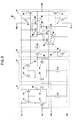
- FIG. 1 shows a structure of an operational amplification circuit according to the first embodiment of the present invention.
- the explanation will be given of the structure and the operation of the operational amplification circuit 10 with reference to FIG. 1.
- the operational amplification circuit 10 of the first embodiment is provided with a first differential amplification circuit 11, a second differential amplification circuit 12, a first level shift circuit 13, a second level shift circuit 14, a first current source I1, a second current source I2 and an output circuit 15.
- the second differential amplification circuit 12 is equivalent to the second differential amplification circuit 32. That is, the first differential amplification circuit 31 varies level of an output voltage from the node N1 in accordance with the voltage difference between the IN1 and the IN2.
- the second differential amplification circuit 32 varies level of an output voltage from the node N2 in accordance with the voltage difference between the IN1 and the IN2 though ranges of the output voltages are different.
- the node N1 of the first differential amplification circuit 11 and the node N2 of the second differential amplification circuit 12 are connected with the first level shift circuit 13 and the second level shift circuit 14, respectively.
- the first level shift circuit 13 consists of a PMOS 59 and a NMOS 60.
- the node N1 in the first differential amplification circuit 11 is connected with a gate of the PMOS 59 of which a source is connected with the V DD .
- a drain of the PMOS 59 is connected with a drain and a gate of the NMOS 60 of which a source is connected with the GND.
- the second level shift circuit 14 consists of a PMOS 61 and a NMOS 62.
- the node N2 of the second differential amplification circuit 12 is connected with a gate of the NMOS 62 of which a source is connected with the GND.
- a drain of the NMOS 62 is connected with a drain and a gate of the PMOS 61 of which a source is connected with the V DD .
- the output circuit 15 consists of a PMOS 63 and a NMOS 64.
- a source of the PMOS 63 and a source of the NMOS 64 are connected with the V DD and the GND, respectively.
- a gate of the NMOS 64 is connected with a connection point (node N3) between drains of the PMOS 59 and the NMOS 60 in the first level shift circuit 13, and a gate of the PMOS 63 is connected with a connection point (node N4) between drains of the PMOS 61 and the NMOS 62 in the second level shift circuit 14.
- a drain of the PMOS 63 is connected with a drain of the NMOS 64, and an output of the operational amplification circuit 10 is delivered from this connection point.
- the current source I1 is provided between the node N3 connected with the gate of the NMOS 64 and the V DD .
- the current source I2 is arranged between the node N4 and the GND.
- the first level shift circuit 13 in this operational amplification circuit independently, outputs a voltage of a level close to the V DD level to the gate of the NMOS 64 when a voltage close to the GND is applied to the gate of the PMOS 59, and outputs a voltage with a level close to the GND level to the gate of the NMOS 64 when a voltage close to the GND is applied to the gate of the PMOS 59.
- the current source I1 is provided between the node N3 and the V DD , so that a voltage, corresponding to a current value of the current source I1, is produced on the node N3 when the PMOS 59 in the first level shift circuit 13 becomes completely off. That is, in the operational amplification circuit 10, there is no case that a voltage of the GND level is applied to the gate of the NMOS 64 though the PMOS 59 is controlled to be in the off-state by the output of the first differential amplification circuit 11.
- the second level shift circuit 14 outputs a voltage of a level close to the GND level from the node N4 when a voltage of a level close to the V DD level is applied to the gate of the NMOSes 62, and outputs a voltage of a level close to the V DD level from the node N4 when a voltage of a level close to the GND level is applied to the gate of the NMOS 62.
- the current source I2 is provided between the node N4 and the GND, so that there is no case in that a voltage of the V DD level, that is, a voltage to control the PMOS 63 to be in an off-state is applied to the node N4.
- the operational amplification circuit 10 operates normally in this case.
- FIG. 2 shows a structure of an operational amplification circuit according to the second embodiment of the present invention.
- the explanation will be given of the structure and the operation of the operational amplification circuit 20 with reference to FIG. 2.
- the operational amplification circuit 20 is provided with a first differential amplification circuit 21, a second differential amplification circuit 22, a level shift circuit 23, a output circuit 24 and a current source I5.
- the first differential amplification circuit 21 has the same structure as the first differential operational circuit 11 in the first embodiment.
- the second differential amplification circuit 22 also has the same structure as the first differential amplification circuit 11 in the first embodiment. However, a gate of the NMOS 54' in the second differential amplification circuit 22, which is a transistor corresponding to the NMOS 54 in the first differential amplification circuit 21 of the first embodiment, is supplied with a signal from not the IN2 but the IN1. And, a gate of the NMOS 53' in the second differential amplification circuit 22, which is a transistor corresponding to the NMOS 53 in the first differential amplification circuit 21, is supplied with a signal from not the IN1 but the IN2.
- the second differential amplification circuit 22 outputs a voltage of a level close to the GND level is generated at the node N6 when a voltage with a level close to the V DD level is generated at the node N5 in the first differential amplification circuit 21. And, the second differential amplification circuit 22 outputs a voltage with a level close to the V DD level is generated at the node N6 when a voltage with a level close to the GND level is generated at the node N5 in the first differential amplification circuit 21.
- the node N5 of the first differential amplification circuit 21 is connected with a gate of the PMOS 59 in the level shift circuit 23 which has the same structure as the first level circuit 13 of the first embodiment.
- a connection point (node N7) between drains of the PMOS 59 and the NMOS 60 in the level shift circuit 23 is connected with a gate of the NMOS 64 in the output circuit 24. Then, the current source I5 is provided between the node N7 connected with the gate of the NMOS 64 and the V DD .
- the node N6 of the second differential amplification circuit 22 is connected with the gate of the PMOS 63 in the output circuit 24.
- the PMOS 63 which is one MOS in the output circuit 24 is controlled directly by the output of the second differential amplification circuit 22, and the NMOS 64 which is the other MOS is controlled by the voltage at the node N7, namely, by the converted output of the first differential amplification circuit 21 with the level shift circuit 23 and the current source I5.
- the operational amplification circuit 20 is structured so as to set a voltage range applied to the gate of the NMOS 64 by a current value of the current source I5.
- the operational amplification circuit 20 is easy to design in a manner that the two MOSes are controlled not to be in the off-state together, similarly to the operational amplification circuit 10.
- the operational amplification circuit 20 also operates normally in this case.
- the second operational amplification circuit 20 is provided with a first phase compensation circuit 25, a second phase compensation circuit 26, a PMOS 61 and a NMOS 71.
- the first phase compensation circuit 25 consists of a capacitor C1 and three MOSes (NMOSes 68, 69, a PMOS 70) which function as resistance elements, and is provided between the node N6 of the second differential amplification circuit 22 and the output terminal OUT.
- the second phase compensation circuit 26 has the same structure as the first phase compensation circuit 25, and is provided between the node N 5 of the first differential amplification circuit 21 and the output terminal OUT.
- the operational amplification circuit 20 can perform an amplification without an oscillation because these phase compensation circuits 25, 26 are provided.
- the PMOS 61 and the NMOS 71 are provided to stop the operation of the operational amplification circuit 20 when the operational amplification circuit 20 is not used. As shown in FIG. 2, a source and a drain of the PMOS 61 are connected with the V DD and the gate of the PMOS 63, respectively. And, a source and a drain of the NMOS 71 are connected with the GND and the gate of the NMOS 64, respectively.
- Signals PDN, PD are supplied to the gates of the PMOS 61 and the NMOS 71 from outer circuits not shown, respectively.
- the PMOS 61 and the NMOS 71 are controlled to be in the off-state together by these signals when the operational amplification circuit 20 operates.
- the PMOS 61 and the NMOS 71 are controlled to be in the on-state together by theses signals.
- the PMOS 63 and the NMOS 64 in the output circuit 24 become the off-state together, and the operation of the operational amplification circuit 20 is stopped.
- the operational amplification circuit 20 is provided with a circuit for stopping the operation of the output circuit 24, so that if an apparatus which has a long time unnecessary to operate, such as an apparatus related to communications is structured with the operational amplification circuit 20, an apparatus with a low consumption power can be obtained.
Landscapes
- Engineering & Computer Science (AREA)
- Power Engineering (AREA)
- Physics & Mathematics (AREA)
- Nonlinear Science (AREA)
- Amplifiers (AREA)
Claims (4)
- Operationsverstärkerschaltung (10), die folgendes aufweist:eine erste Differentialverstärkerschaltung (11), die einen ersten N-Kanal-MOS-Transistor (53) hat, von welchem ein Gateanschluß mit einem ersten Eingangsanschluß verbunden ist, und einen zweiten N-Kanal-MOS-Transistor (54), von welchem ein Gateanschluß mit einem zweiten Eingangsanschluß verbunden ist, und die eine Spannung gemäß einer Spannungsdifferenz zwischen dem ersten Eingangsanschluß und dem zweiten Eingangsanschluß ausgibt;eine zweite Differentialverstärkerschaltung (12), die einen ersten P-Kanal-MOS-Transistor (55) hat, von welchem ein Gateanschluß mit dem ersten Eingangsanschluß verbunden ist, und einen zweiten P-Kanal-MOS-Transistor (56), von welchem ein Gateanschluß mit dem zweiten Eingangsanschluß verbunden ist, und die eine Spannung gemäß der Spannungsdifferenz zwischen dem ersten Eingangsanschluß und dem zweiten Eingangsanschluß ausgibt;eine erste Pegelverschiebungsschaltung (13), die einen dritten P-Kanal-MOS-Transistor (59) hat, von welchem ein Gateanschluß mit der Spannung versorgt wird, die von der ersten Differentialverstärkerschaltung ausgegeben wird, und einen dritten N-Kanal-MOS-Transistor (60), und die eine Spannung ausgibt, die durch Verschieben eines Pegels der an den dritten P-Kanal-MOS-Transistor (59) angelegten Spannung erhalten wird;eine zweite Pegelverschiebungsschaltung (14), die einen vierten N-Kanal-MOS-Transistor (62) hat, von welchem ein Gateanschluß mit der Spannung versorgt wird, die von der zweiten Differentialverstärkerschaltung ausgegeben wird, und einen vierten P-Kanal-MOS-Transistor (61), und die eine Spannung ausgibt, die durch Verschieben eines Pegels der an den vierten N-Kanal-MOS-Transistor (62) angelegten Spannung erhalten wird;eine erste Stromquelle, die einen ersten Strom mit vorbestimmtem Pegel zum dritten N-Kanal-MOS-Transistor (60) in der ersten Pegelverschiebungsschaltung (13) zuführt, und wobei die erste Stromquelle zum dritten P-Kanal-MOS-Transistor (59) parallelgeschaltet ist;eine zweite Stromquelle, die einen zweiten Strom mit vorbestimmtem Pegel zum vierten P-Kanal-MOS-Transistor (61) in der zweiten Pegelverschiebungsschaltung (14) zuführt, und wobei die zweite Stromquelle zum vierten N-Kanal-MOS-Transistor (62) parallelgeschaltet ist; undeine Ausgangsschaltung (15), die einen fünften P-Kanal-MOS-Transistor (63) hat, von welchem ein Gateanschluß mit der Spannung versorgt wird, die von der zweiten Pegelverschiebungsschaltung (14) ausgegeben wird, und einen fünften N-Kanal-MOS-Transistor (64), von welchem ein Gateanschluß mit der Spannung versorgt wird, die von der ersten Pegelverschiebungsschaltung (13) ausgegeben wird, und die eine Spannung gemäß Zuständen des fünften P-Kanal-MOS-Transistors (63) und des fünften N-Kanal-MOS-Transistors (64) ausgibt.
- Operationsverstärkerschaltung (20), die folgendes aufweist:eine erste Differentialverstärkerschaltung (21), die einen ersten N-Kanal-MOS-Transistor (53) hat, von welchem ein Gateanschluß mit einem ersten Eingangsanschluß verbunden ist, und einen zweiten N-Kanal-MOS-Transistor (54), von welchem ein Gateanschluß mit einem zweiten Eingangsanschluß verbunden ist, und die eine Spannung, die eine selbe Phase wie eine Spannungsdifferenz zwischen dem ersten Eingangsanschluß und dem zweiten Eingangsanschluß hat, gemäß der Spannungsdifferenz ausgibt;eine zweite Differentialverstärkerschaltung (22), die einen dritten N-Kanal-MOS-Transistor (54') hat, von welchem ein Gateanschluß mit dem ersten Eingangsanschluß verbunden ist, und einen vierten N-Kanal-MOS-Transistor (53'), von welchem ein Gateanschluß mit dem zweiten Eingangsanschluß verbunden ist, und die eine Spannung, die eine entgegengesetzte Phase zur Spannungsdifferenz zwischen dem ersten Eingangsanschluß und dem zweiten Eingangsanschluß hat, gemäß der Spannungsdifferenz ausgibt;eine Pegelverschiebungsschaltung (23), die einen ersten P-Kanal-MOS-Transistor (59) hat, von welchem ein Gateanschluß mit der Spannung versorgt wird, die von der ersten Differentialverstärkerschaltung (21) ausgegeben wird, und einen fünften N-Kanal-MOS-Transistor (60), und die eine Spannung ausgibt, die durch Verschieben eines Pegels der an den ersten P-Kanal-MOS-Transistor (59) angelegten Spannung erhalten wird;eine Stromquelle, die einen Strom mit vorbestimmtem Pegel zum fünften N-Kanal-MOS-Transistor (60) in der Pegelverschiebungsschaltung (23) zuführt, wobei die Stromquelle zum ersten P-Kanal-MOS-Transistor (59) parallelgeschaltet ist; undeine Ausgangsschaltung (24), die einen zweiten P-Kanal-MOS-Transistor (63) hat, von welchem ein Gateanschluß mit der Spannung versorgt wird, die von der zweiten Differentialverstärkerschaltung (22) ausgegeben wird, und einen sechsten N-Kanal-MOS-Transistor (64), von welchem ein Gateanschluß mit der Spannung versorgt wird, die von der Pegelverschiebungsschaltung (23) ausgegeben wird, und die eine Spannung gemäß Zuständen des zweiten P-Kanal-MOS-Transistors (63) und des sechsten N-Kanal-MOS-Transistors (64) ausgibt.
- Operationsverstärkerschaltung (10) nach Anspruch 1, die weiterhin folgendes aufweist:
eine Abschaltschaltung zum Steuern des fünften N-Kanal-MOS-Transistors (64) in der Ausgangsschaltung (15), um in einem Aus-Zustand zu sein, indem eine Spannung variiert wird, die an einen Gateanschluß des fünften N-Kanal-MOS-Transistors (64) angelegt ist, und zum Steuern des fünften P-Kanal-MOS-Transistors (63) in der Ausgangsschaltung (15), um in einem Aus-Zustand zu sein, indem eine Spannung variiert wird, die an einen Gateanschluß des fünften P-Kanal-MOS-Transistors (63) angelegt ist, wenn ein vorbestimmtes Steuersignal eingegeben wird. - Operationsverstärkerschaltung (20) nach Anspruch 2, die weiterhin folgendes aufweist:
eine Abschaltschaltung zum Steuern des sechsten N-Kanal-MOS-Transistors (64) in der Ausgangsschaltung (24), um in einem Auf-Zustand zu sein, indem eine Spannung variiert wird, die an einen Gateanschluß des sechsten N-Kanal-MOS-Transistors (64) angelegt ist, und zum Steuern des zweiten P-Kanal-MOS-Transistors (63) in der Ausgangsschaltung (24), um in einem Aus-Zustand zu sein, indem eine Spannung variiert wird, die an einen Gateanschluß des zweiten P-Kanal-MOS-Transistors (63) angelegt ist, wenn ein vorbestimmtes Steuersignal eingegeben wird.
Applications Claiming Priority (3)
| Application Number | Priority Date | Filing Date | Title |
|---|---|---|---|
| JP8036190A JPH09232883A (ja) | 1996-02-23 | 1996-02-23 | 演算増幅回路 |
| JP3619096 | 1996-02-23 | ||
| JP36190/96 | 1996-02-23 |
Publications (2)
| Publication Number | Publication Date |
|---|---|
| EP0792013A1 EP0792013A1 (de) | 1997-08-27 |
| EP0792013B1 true EP0792013B1 (de) | 2001-08-08 |
Family
ID=12462814
Family Applications (1)
| Application Number | Title | Priority Date | Filing Date |
|---|---|---|---|
| EP97102413A Expired - Lifetime EP0792013B1 (de) | 1996-02-23 | 1997-02-14 | Operationsverstärkerschaltung |
Country Status (6)
| Country | Link |
|---|---|
| US (1) | US5907259A (de) |
| EP (1) | EP0792013B1 (de) |
| JP (1) | JPH09232883A (de) |
| KR (1) | KR970063901A (de) |
| CN (1) | CN1084085C (de) |
| DE (1) | DE69705977T2 (de) |
Families Citing this family (36)
| Publication number | Priority date | Publication date | Assignee | Title |
|---|---|---|---|---|
| JP3435309B2 (ja) * | 1997-06-04 | 2003-08-11 | 株式会社東芝 | バッファアンプ |
| KR100474994B1 (ko) * | 1997-08-13 | 2005-06-17 | 삼성전자주식회사 | 레일 연산 증폭 출력 장치 |
| JP3416479B2 (ja) * | 1997-09-03 | 2003-06-16 | キヤノン株式会社 | 演算増幅器 |
| IT1296028B1 (it) * | 1997-09-25 | 1999-06-04 | Sgs Thomson Microelectronics | Stadio di uscita a basso offset per comparatori di precisione |
| JP4158214B2 (ja) * | 1997-10-31 | 2008-10-01 | 沖電気工業株式会社 | 半導体集積回路 |
| JP3875392B2 (ja) * | 1998-02-23 | 2007-01-31 | 株式会社東芝 | 演算増幅器 |
| SE9801117D0 (sv) * | 1998-03-30 | 1998-03-30 | Astra Ab | Electrical device |
| US6259316B1 (en) * | 1998-05-29 | 2001-07-10 | Texas Instruments Incorporated | Low voltage buffer amplifier for high speed sample and hold applications |
| US6069532A (en) * | 1998-07-20 | 2000-05-30 | Lucent Technologies Inc. | Technique for designing a bias circuit for an amplifier in an integrated circuit device |
| US6166592A (en) * | 1998-07-31 | 2000-12-26 | Lucent Technologies Inc. | Linear CMOS transconductor with rail-to-rail compliance |
| US6107883A (en) * | 1998-09-10 | 2000-08-22 | Seiko Epson Corporation | High gain, high speed rail-to-rail amplifier |
| US6066985A (en) * | 1998-09-10 | 2000-05-23 | Seiko Epson Corporation | Large swing input/output analog buffer |
| US6127891A (en) * | 1999-04-05 | 2000-10-03 | National Semiconductor Corporation | Low voltage class AB amplifier with gain boosting |
| US6236269B1 (en) * | 1999-10-07 | 2001-05-22 | National Semiconductor Corporation | Complementary CMOS differential amplifier circuit |
| US6362665B1 (en) | 1999-11-19 | 2002-03-26 | Intersil Americas Inc. | Backwards drivable MOS output driver |
| JP2002076800A (ja) * | 2000-08-30 | 2002-03-15 | Nec Corp | 電圧減算・加算回路及びそれを実現するmos差動増幅回路 |
| US6433637B1 (en) * | 2001-03-23 | 2002-08-13 | National Semiconductor Corporation | Single cell rail-to-rail input/output operational amplifier |
| US6600363B2 (en) | 2001-04-05 | 2003-07-29 | Cornell Research Foundation, Inc. | Folded floating-gate differential pair amplifier |
| KR100542685B1 (ko) * | 2001-06-18 | 2006-01-16 | 매그나칩 반도체 유한회사 | 출력버퍼용 연산 트랜스컨덕턴스 증폭기 |
| US6384685B1 (en) * | 2001-06-28 | 2002-05-07 | Sunplus Technology Co., Ltd. | Complementary metal oxide semiconductor class AB amplifier |
| US6566952B1 (en) * | 2001-07-27 | 2003-05-20 | Cypress Semiconductor Corp. | Operational amplifier with extended output voltage range |
| JP3847241B2 (ja) | 2002-10-01 | 2006-11-22 | Necエレクトロニクス株式会社 | 演算増幅器 |
| CN100525086C (zh) * | 2002-11-26 | 2009-08-05 | 三菱电机株式会社 | 驱动电路 |
| JP2004222015A (ja) * | 2003-01-16 | 2004-08-05 | Fuji Electric Device Technology Co Ltd | 増幅回路 |
| EP1441439A1 (de) * | 2003-01-23 | 2004-07-28 | Infineon Technologies AG | Analogverstärker mit Multiplexierungsfähigkeit |
| JP2004317857A (ja) * | 2003-04-17 | 2004-11-11 | Nec Yamagata Ltd | 駆動回路及び表示装置 |
| US6933781B2 (en) * | 2003-04-30 | 2005-08-23 | Intel Corporation | Large gain-bandwidth amplifier, method, and system |
| KR100620662B1 (ko) | 2003-09-26 | 2006-09-19 | 엔이씨 일렉트로닉스 가부시키가이샤 | 차동 에이비 클래스 증폭 회로 및 이를 이용한 구동 회로 |
| TWI307212B (en) * | 2005-05-06 | 2009-03-01 | Novatek Microelectronics Corp | Amplfier device and transformation device thereof |
| JP4861791B2 (ja) * | 2006-10-27 | 2012-01-25 | ルネサスエレクトロニクス株式会社 | 演算増幅器及び表示装置 |
| TWI321901B (en) * | 2006-11-10 | 2010-03-11 | Orise Technology Co Ltd | Rail-to-rail class-ab operational amplifier |
| US7859338B2 (en) * | 2007-07-26 | 2010-12-28 | Broadcom Corporation | Compact low-power class AB amplifier |
| CN101471634B (zh) * | 2007-12-29 | 2011-05-11 | 瑞昱半导体股份有限公司 | 输出级电路以及使用其的运算放大器 |
| TWI360944B (en) * | 2008-12-29 | 2012-03-21 | Princeton Technology Corp | Operational amplifier and method for reducing offs |
| CN101800519B (zh) * | 2009-02-09 | 2015-02-04 | 普诚科技股份有限公司 | 运算放大器及降低运算放大器的偏移电压的方法 |
| US9007096B1 (en) * | 2014-07-07 | 2015-04-14 | Xilinx, Inc. | High-speed analog comparator |
Family Cites Families (6)
| Publication number | Priority date | Publication date | Assignee | Title |
|---|---|---|---|---|
| JP2543872B2 (ja) * | 1986-08-13 | 1996-10-16 | 株式会社東芝 | 増幅回路 |
| US5083051A (en) * | 1990-02-26 | 1992-01-21 | Motorola, Inc. | Output driver circuit with improved output stage biasing |
| JPH04310006A (ja) * | 1991-04-08 | 1992-11-02 | Nippon Telegr & Teleph Corp <Ntt> | 演算増幅回路 |
| US5142244A (en) * | 1991-05-06 | 1992-08-25 | Harris Corporation | Full range input/output comparator |
| JP3320434B2 (ja) * | 1991-11-28 | 2002-09-03 | 沖電気工業株式会社 | 演算増幅回路 |
| US5194824A (en) * | 1992-01-23 | 1993-03-16 | Intel Corporation | 5V Rail-rail unity gain amplifier driving high capacitive load |
-
1996
- 1996-02-23 JP JP8036190A patent/JPH09232883A/ja active Pending
-
1997
- 1997-02-14 EP EP97102413A patent/EP0792013B1/de not_active Expired - Lifetime
- 1997-02-14 DE DE69705977T patent/DE69705977T2/de not_active Expired - Fee Related
- 1997-02-21 US US08/804,259 patent/US5907259A/en not_active Expired - Lifetime
- 1997-02-21 KR KR1019970005369A patent/KR970063901A/ko not_active Withdrawn
- 1997-02-22 CN CN97102818A patent/CN1084085C/zh not_active Expired - Fee Related
Also Published As
| Publication number | Publication date |
|---|---|
| CN1084085C (zh) | 2002-05-01 |
| DE69705977T2 (de) | 2002-04-04 |
| US5907259A (en) | 1999-05-25 |
| JPH09232883A (ja) | 1997-09-05 |
| CN1165427A (zh) | 1997-11-19 |
| EP0792013A1 (de) | 1997-08-27 |
| KR970063901A (ko) | 1997-09-12 |
| DE69705977D1 (de) | 2001-09-13 |
Similar Documents
| Publication | Publication Date | Title |
|---|---|---|
| EP0792013B1 (de) | Operationsverstärkerschaltung | |
| US4554515A (en) | CMOS Operational amplifier | |
| US5754078A (en) | Operational amplifier for class B amplification | |
| US4484148A (en) | Current source frequency compensation for a CMOS amplifier | |
| US5177450A (en) | Cmos power amplifier | |
| JP3320434B2 (ja) | 演算増幅回路 | |
| KR19990083306A (ko) | 연산증폭방법및연산증폭기 | |
| US7116172B2 (en) | High-swing folded cascode having a novel gain-boost amplifier | |
| US7999617B2 (en) | Amplifier circuit | |
| US7098736B2 (en) | Amplifier circuit | |
| CA1158727A (en) | Driver circuit having reduced cross-over distortion | |
| US7521994B2 (en) | Three-stage amplifier | |
| US20050200411A1 (en) | Differential amplifier without common mode feedback | |
| US5424681A (en) | Wide range operational amplifier | |
| US7755428B2 (en) | Amplifying circuit | |
| JPH11510672A (ja) | 能動ブートストラップ式利得向上技術を適用した増幅器 | |
| US20060012429A1 (en) | Self biased differential amplifier | |
| US6937100B2 (en) | Amplifier circuit with common mode feedback | |
| US6496066B2 (en) | Fully differential operational amplifier of the folded cascode type | |
| JPWO2006132315A1 (ja) | バッファ回路 | |
| US4970471A (en) | Gallium arsenide class AB output stage | |
| JP2000278058A (ja) | 増幅回路 | |
| US7012465B2 (en) | Low-voltage class-AB output stage amplifier | |
| JP3341945B2 (ja) | 演算増幅器 | |
| KR20050073755A (ko) | 차동증폭기 |
Legal Events
| Date | Code | Title | Description |
|---|---|---|---|
| PUAI | Public reference made under article 153(3) epc to a published international application that has entered the european phase |
Free format text: ORIGINAL CODE: 0009012 |
|
| AK | Designated contracting states |
Kind code of ref document: A1 Designated state(s): DE FR GB NL |
|
| 17P | Request for examination filed |
Effective date: 19970922 |
|
| 17Q | First examination report despatched |
Effective date: 19991202 |
|
| GRAG | Despatch of communication of intention to grant |
Free format text: ORIGINAL CODE: EPIDOS AGRA |
|
| GRAG | Despatch of communication of intention to grant |
Free format text: ORIGINAL CODE: EPIDOS AGRA |
|
| GRAH | Despatch of communication of intention to grant a patent |
Free format text: ORIGINAL CODE: EPIDOS IGRA |
|
| GRAH | Despatch of communication of intention to grant a patent |
Free format text: ORIGINAL CODE: EPIDOS IGRA |
|
| GRAA | (expected) grant |
Free format text: ORIGINAL CODE: 0009210 |
|
| AK | Designated contracting states |
Kind code of ref document: B1 Designated state(s): DE FR GB NL |
|
| REF | Corresponds to: |
Ref document number: 69705977 Country of ref document: DE Date of ref document: 20010913 |
|
| ET | Fr: translation filed | ||
| PGFP | Annual fee paid to national office [announced via postgrant information from national office to epo] |
Ref country code: FR Payment date: 20011130 Year of fee payment: 6 |
|
| REG | Reference to a national code |
Ref country code: GB Ref legal event code: IF02 |
|
| PLBE | No opposition filed within time limit |
Free format text: ORIGINAL CODE: 0009261 |
|
| STAA | Information on the status of an ep patent application or granted ep patent |
Free format text: STATUS: NO OPPOSITION FILED WITHIN TIME LIMIT |
|
| 26N | No opposition filed | ||
| PGFP | Annual fee paid to national office [announced via postgrant information from national office to epo] |
Ref country code: GB Payment date: 20030212 Year of fee payment: 7 |
|
| PGFP | Annual fee paid to national office [announced via postgrant information from national office to epo] |
Ref country code: NL Payment date: 20030226 Year of fee payment: 7 |
|
| PGFP | Annual fee paid to national office [announced via postgrant information from national office to epo] |
Ref country code: DE Payment date: 20030227 Year of fee payment: 7 |
|
| PG25 | Lapsed in a contracting state [announced via postgrant information from national office to epo] |
Ref country code: GB Free format text: LAPSE BECAUSE OF NON-PAYMENT OF DUE FEES Effective date: 20040214 |
|
| PG25 | Lapsed in a contracting state [announced via postgrant information from national office to epo] |
Ref country code: NL Free format text: LAPSE BECAUSE OF NON-PAYMENT OF DUE FEES Effective date: 20040901 Ref country code: DE Free format text: LAPSE BECAUSE OF NON-PAYMENT OF DUE FEES Effective date: 20040901 |
|
| GBPC | Gb: european patent ceased through non-payment of renewal fee |
Effective date: 20040214 |
|
| PG25 | Lapsed in a contracting state [announced via postgrant information from national office to epo] |
Ref country code: FR Free format text: LAPSE BECAUSE OF NON-PAYMENT OF DUE FEES Effective date: 20041029 |
|
| NLV4 | Nl: lapsed or anulled due to non-payment of the annual fee |
Effective date: 20040901 |
|
| REG | Reference to a national code |
Ref country code: FR Ref legal event code: ST |
|
| PG25 | Lapsed in a contracting state [announced via postgrant information from national office to epo] |
Ref country code: FR Free format text: LAPSE BECAUSE OF NON-PAYMENT OF DUE FEES Effective date: 20030228 |