EP0793103A2 - Halbleiter-Beschleunigungssensor - Google Patents
Halbleiter-Beschleunigungssensor Download PDFInfo
- Publication number
- EP0793103A2 EP0793103A2 EP97301298A EP97301298A EP0793103A2 EP 0793103 A2 EP0793103 A2 EP 0793103A2 EP 97301298 A EP97301298 A EP 97301298A EP 97301298 A EP97301298 A EP 97301298A EP 0793103 A2 EP0793103 A2 EP 0793103A2
- Authority
- EP
- European Patent Office
- Prior art keywords
- semiconductor
- semiconductor wafer
- strain sensitive
- sensitive section
- diffused resistors
- Prior art date
- Legal status (The legal status is an assumption and is not a legal conclusion. Google has not performed a legal analysis and makes no representation as to the accuracy of the status listed.)
- Withdrawn
Links
Images


Classifications
-
- B—PERFORMING OPERATIONS; TRANSPORTING
- B81—MICROSTRUCTURAL TECHNOLOGY
- B81B—MICROSTRUCTURAL DEVICES OR SYSTEMS, e.g. MICROMECHANICAL DEVICES
- B81B7/00—Microstructural systems; Auxiliary parts of microstructural devices or systems
- B81B7/0032—Packages or encapsulation
- B81B7/0077—Other packages not provided for in groups B81B7/0035 - B81B7/0074
-
- G—PHYSICS
- G01—MEASURING; TESTING
- G01P—MEASURING LINEAR OR ANGULAR SPEED, ACCELERATION, DECELERATION, OR SHOCK; INDICATING PRESENCE, ABSENCE, OR DIRECTION, OF MOVEMENT
- G01P1/00—Details of instruments
- G01P1/02—Housings
- G01P1/023—Housings for acceleration measuring devices
-
- G—PHYSICS
- G01—MEASURING; TESTING
- G01P—MEASURING LINEAR OR ANGULAR SPEED, ACCELERATION, DECELERATION, OR SHOCK; INDICATING PRESENCE, ABSENCE, OR DIRECTION, OF MOVEMENT
- G01P15/00—Measuring acceleration; Measuring deceleration; Measuring shock, i.e. sudden change of acceleration
- G01P15/02—Measuring acceleration; Measuring deceleration; Measuring shock, i.e. sudden change of acceleration by making use of inertia forces using solid seismic masses
- G01P15/08—Measuring acceleration; Measuring deceleration; Measuring shock, i.e. sudden change of acceleration by making use of inertia forces using solid seismic masses with conversion into electric or magnetic values
- G01P15/12—Measuring acceleration; Measuring deceleration; Measuring shock, i.e. sudden change of acceleration by making use of inertia forces using solid seismic masses with conversion into electric or magnetic values by alteration of electrical resistance
- G01P15/123—Measuring acceleration; Measuring deceleration; Measuring shock, i.e. sudden change of acceleration by making use of inertia forces using solid seismic masses with conversion into electric or magnetic values by alteration of electrical resistance by piezo-resistive elements, e.g. semiconductor strain gauges
-
- G—PHYSICS
- G01—MEASURING; TESTING
- G01P—MEASURING LINEAR OR ANGULAR SPEED, ACCELERATION, DECELERATION, OR SHOCK; INDICATING PRESENCE, ABSENCE, OR DIRECTION, OF MOVEMENT
- G01P15/00—Measuring acceleration; Measuring deceleration; Measuring shock, i.e. sudden change of acceleration
- G01P15/02—Measuring acceleration; Measuring deceleration; Measuring shock, i.e. sudden change of acceleration by making use of inertia forces using solid seismic masses
- G01P15/08—Measuring acceleration; Measuring deceleration; Measuring shock, i.e. sudden change of acceleration by making use of inertia forces using solid seismic masses with conversion into electric or magnetic values
- G01P2015/0805—Measuring acceleration; Measuring deceleration; Measuring shock, i.e. sudden change of acceleration by making use of inertia forces using solid seismic masses with conversion into electric or magnetic values being provided with a particular type of spring-mass-system for defining the displacement of a seismic mass due to an external acceleration
- G01P2015/0822—Measuring acceleration; Measuring deceleration; Measuring shock, i.e. sudden change of acceleration by making use of inertia forces using solid seismic masses with conversion into electric or magnetic values being provided with a particular type of spring-mass-system for defining the displacement of a seismic mass due to an external acceleration for defining out-of-plane movement of the mass
- G01P2015/0825—Measuring acceleration; Measuring deceleration; Measuring shock, i.e. sudden change of acceleration by making use of inertia forces using solid seismic masses with conversion into electric or magnetic values being provided with a particular type of spring-mass-system for defining the displacement of a seismic mass due to an external acceleration for defining out-of-plane movement of the mass for one single degree of freedom of movement of the mass
- G01P2015/0828—Measuring acceleration; Measuring deceleration; Measuring shock, i.e. sudden change of acceleration by making use of inertia forces using solid seismic masses with conversion into electric or magnetic values being provided with a particular type of spring-mass-system for defining the displacement of a seismic mass due to an external acceleration for defining out-of-plane movement of the mass for one single degree of freedom of movement of the mass the mass being of the paddle type being suspended at one of its longitudinal ends
Definitions
- the present invention particularly relates to an acceleration sensor and a pressure sensor in a semiconductor device for converting a displacement into electric signals by utilising piezoresistance effect inherent to a semiconductor crystal such as silicon.
- a semiconductor acceleration sensor has been manufactured by means of film formation or etching on a semiconductor wafer (See IEEE Transactions on Electron Devices, Vol ED-26, No. 12, Dec 1979, for example).
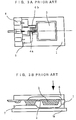
- Fig. 4A is a view showing a semiconductor acceleration sensor according to micro machining disclosed in Japanese patent laid-open publication No. 1-302167, wherein a groove portion 35 is formed in the vicinity of a supporting body 9 of the cantilever 2 by etching to provide a thin portion 36.
- Diffused resistors 4c, 4d, 4e and 4f are provided on the top face of the sensor to constitute a bridge circuit 50.
- the diffused resistors 4c and 4f function as reference resistors and are provided on the top face of the supporting body 9.
- the diffused resistors 4d and 4e function as variable resistors for detecting a quantity of deformation of the thin portion 36 and are provided at positions orthogonal to the reference resistors.
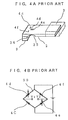
- Fig. 4B shows a detection circuit of the device shown in Fig. 4A.
- the thin portion 36 shown in Fig. 4A must be formed in order to improve detection sensitivity, thereby deteriorating the overall mechanical strength.
- the thickness of the thin portion 36 relates to detection sensitivity, and conditions for composition, temperature and stirring of etchant must be strictly managed in order to obtain an uniform thickness when forming the thin portion 36 by etching, increasing manufacturing steps such as masking pattern formation.
- an area of the top surface of the acceleration sensor becomes large, a number of sensors taken out from, e.g., one silicon substrate is limited and the manufacturing cost is hard to be reduced because the diffused resistors 4a and 4b are provided on the top surface of the acceleration sensor and the dead-weight 3 is formed as shown in Fig. 3A.
- a predetermined value is required for a width of the cantilever 2, ie, the width from the front side to the other side in the drawing in order to maintain the strength of the thin portion 36 in the acceleration sensor in Fig. 4A. Therefore, an area of the top face of the sensor can not be reduced as in the acceleration sensor shown in Fig. 3A to limit a number of sensors taken out from the semiconductor wafer, and the cost down is difficult.
- the diffused resistors 4 for detecting the acceleration are provided on a surface to which acceleration of the acceleration sensor is applied, the diffused resistors 4 must be so disposed as to enlarge a difference in resistance value between the reference resistors and the variable resistors provided on the top face of the supporting body 9.
- an object of the present invention is to obtain inexpensive semiconductor acceleration sensor and pressure sensor with which manufacturing is facilitated and a large number of sensors can be produced from one semiconductor wafer.
- diffused resistors 4 are provided on the side surface of a sensor in order to produce a large number of sensors from one semiconductor wafer.
- provision of a detection means for detecting a quantity of displacement on the side surface of the sensor can obtain a highly-accurate inexpensive sensor with the reduced number of processing steps using no etching process.
- a semiconductor device which has a good yield and a semiconductor acceleration sensor can be supplied.
- a semiconductor substrate 11 has a rectangular parallelepiped shape, having upper and lower opposing surfaces joined by four side edges 100, and diffused resistors 4 and output terminals 8 electrically connected with the diffused resistors 4 are disposed on a side edge surface 100 that is one surface of the semiconductor substrate 11.
- An amplification circuit, a temperature compensation circuit or a filter circuit may be provided on the side surface 100 in the semiconductor substrate 11. Also, they may be provided on any other form of the device.
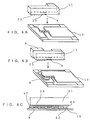
- Fig. 2A is a top plan view of the semiconductor acceleration sensor and Fig. 2B is a side view of the same.
- the semiconductor substrate 11 can be formed into various shapes, it is effective when formed into a rectangular parallelepiped because it can be easily taken out from the semiconductor wafer 12. Moreover, if the thickness Z of the semiconductor substrate 11 is made smaller than the width W of the semiconductor substrate 11, the detection sensitivity can be increased. Note that a portion L2 at which the supporting body 9 and the semiconductor substrate 11 are fixed is a supporting portion and a portion Ll at which these members are not fixed and oscillation is possible is a sensor portion, and these names will be used hereinbelow.
- the configuration made up of the semiconductor substrate 11, the supporting body 9 and the dead-weight 3 shown in Figs. 2 will be referred to as a semiconductor acceleration sensor device.
- a second embodiment comprises a plurality of bridge circuits arranged on a rectangular parallelepiped type structure on a surface having strain sensing portions.
- the strain sensing portions are a portion on which diffused resistors or the like whose resistance values vary in response to strain or stress are formed. According to the structure of this embodiment, a function as a pressure sensor can be obtained by fixing the both ends.
- an end of the supporting body 9 is placed at a position indicated by a in the drawing because sensitivity must be improved. Since a length L of the sensor portion becomes long, sensitivity is thereby increased.
- Positions of diffused resistors are selected in accordance with applications for high acceleration and low acceleration. After selection, wires of any other diffused resistors are not necessary and thereby cut.
- the mounting process can not be easily attained if the thin portion is formed by the conventional etching method. Even if mounting is successfully made, provision of the thin portion having the unnecessary diffused resistors may cause a problem of damage.
- the structure is shaped into a rectangular parallelepiped in the present invention, handling can be readily attained and recognition of right and left sides is unnecessary, facilitating mass production of the device.
- a pressure reference chamber is produced as a structure to detect a difference in pressure using the pressure reference chamber.
- the bridge circuits constituted by the diffused resistors 4 and the output terminals 8 are provided symmetrically with respect to the center of the side surface 100 of the semiconductor substrate 11 in the longitudinal direction. A displacement of the pressure is detected using the diffused resistors 4 by producing the pressure reference chamber on one side of the semiconductor substrate 11.
- the diffused resistors 4 may be arranged in the vicinity of the fixed end at which the stress becomes maximum.
- Fig. 15 shows a fourth embodiment in which the diffused resistors are arranged in the center of the semiconductor substrate 11.
- the diffused resistors are arranged in the center, the right and left sides can not be mistaken in the mounting process to improve the yield and simplify the facility.
- wires electrically connecting between the MOS transistors constituting the electric circuit or the aluminum wires electrically connecting the MOS transistors and polysilicon forming the resistor portion are formed outside the MOS transistors and the polysilicon resistor portion. With this arrangement, wires are formed in the detailed portions.
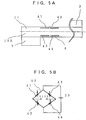
- the diffused resistors 4 are provided at the peripheral portion of the side surface 100 to improve sensitivity. Each wire is therefore disposed inside the diffused resistors 4 constituting the bridge circuit 50.
- Fig. 5B shows the bridge circuit 50 having this configuration.
- the largest characteristic of the bridge circuit according to the present invention is that four diffused resistors are variable.
- the electric circuit according to the invention is twice as powerful as the prior art circuit. Therefore, in the arrangement of the diffused resistors 4 according to the present invention, the diffused resistors 4 are so disposed as to improve sensitivity by utilizing the tensile stress and compressive stress.
- dicing may be enabled for cutting the semiconductor wafer 12. Dicing is carried out in such a manner that a line for scribing is provided to the outer portion of the semiconductor substrate 11 and the semiconductor wafer is cut by dicing with the line for scribing as a reference.
- the acceleration sensor semiconductor devices 101 are arranged in the semiconductor wafer 12.
- the low acceleration device is produced.
- the acceleration sensor for low acceleration is applied for detecting earthquake or virtual reality. Further, it functions as a shock sensor for detecting the drop impact.
- Fig. 7B shows the cut-out surface.
- the semiconductor substrate 11 can be cut out in the dicing method using water as regular cutting liquid, the semiconductor substrate 11 is cut out in the following manner to improve accuracy in this embodiment.
- the electrophoresis phenomenon of the superfine abrasive grain is utilized.
- the superfine silica abrasive grain is used in the cutting liquid.
- the superfine silica abrasive grain is charged negative in the alkali liquid. If the electric field has an effect, the silica therefore migrates toward an anode 13. It does not migrate toward a cathode 14. This phenomenon is shown in Fig. 8.
- the superfine silica abrasive grains are provided at the charged electrode of the anode 13.
- the silica particles 15 of colloidal silica electrically causes absorption phenomenon on the surface of the electrode.
- the absorption layer is continuously formed on the surface of the electrode.
- the absorption layers of the superfine silica abrasive grains can be readily formed by producing the electric field to a blade 16, thus enabling machining with the cutting resistance reduced.
- the structure of the device used in this embodiment is shown in Fig. 9.
- the device is constituted by providing a mechanism for supplying abrasive material to a dicing blade 16 and a power supply 17 for subjecting the dicing blade 16 to electrolysis on the dicing apparatus which is normally used.
- the blade is fixed by a flange 19.
- Colloidal silica that is cutting material is supplied to the blade 16 and the blade 16 is subjected to electrolysis by the direct current power supply 17 to form a silica layer on the blade 16.
- the semiconductor wafer 12 is installed on a chuck 18 and cut by the dicing apparatus.
- the dicing blade 16 moves down on the fixed semiconductor wafer 12 to be brought into contact with the semiconductor wafer 12.
- superfine silica abrasive grains are supplied to the blade as abrasive material.
- the silica particles 15 are adhered to the blade 16.
- the superfine silica abrasive grain has a particle size of 10 nm to 20 nm, and silica having this particle size is charged on the anode 13 and adhered to the dicing blade 16.
- This adhesive layer cuts the semiconductor wafer 12 that is a work to demonstrate an effect, which leads to excellent machining.
- the stable device with the good yield can be supplied without cutting the wires or damaging the diffused layer.
- cast iron is used as bonding material 32 and the dicing blade 16 having diamond particles 31 is used to subject the dicing blade 16 to electrolysis.
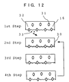
- a non-conductive coat 30 is formed on a surface of the abrasive wheel by electrolysis. The process will be described with reference to Fig. 12.
- the blade 16 is subjected to electrolysis. Cast iron of the bonding material of the blade 16 eludes. It eludes as iron ions 33. Oxidation is started and the non-conductive coat 30 is formed on a surface of the blade 16 by electrolysis. The diamond particles 31 protrude from the blade 16. In this state, cutting is started.
- the apparatus is composed of the structure for subjecting the dicing blade 16 to electrolysis, a cathode attachment 14 provided in the vicinity of the dicing blade 16 and the structure for subjecting the blade 16 to electrolysis using the direct current power supply 17. With this configuration, the semiconductor wafer 12 is cut.
- a dicing tape for fixation which weakens adhesive power by irradiation of ultraviolet rays is used as a means for fixing the semiconductor wafer 12 that is a work, which facilitates detachment and realizes assured fixation.
- the device can be taken out with reduced chipping and layers deformed during machining by cutting in the dicing apparatus.
- the similar characteristics can be obtained by polishing the semiconductor substrate 11.
- layers deformed during machining can be advantageously eliminated by the superfine polishing method such as float polishing.
- the side surface 100 can be uniformly polished from the both sides thereof equalizing distances to the diffused resistors.
- a dead-weight 3 is provided to one end of the semiconductor substrate 11 in order to improve detection sensitivity of the acceleration sensor, as shown in Fig. 7C.
- the dead-weight 3 metal or silicon can be used.
- the dead-weight 3 and the supporting body 9 are fixed to the semiconductor substrate 11.
- the supporting body 9 may be previously fixed to a supporting board 10.
- adhesive is applied to the central position of the dead-weight 3 in advance so that the center of the dead-weight 3 can be set at the position of the center of gravity.
- the adhesive is applied to the center of the dead-weight 3, this process is carried out according to the self-alignment method by which the central position of the dead weight 3 can be easily obtained. Further, the adhesive or any material which can be easily matched with the adhesive may be applied or a film of such material may be formed at a part of the semiconductor board 11 on which the dead-weight 3 is mounted.
- the dead-weight is an important element for obtaining sensitivity. If the sensor itself receives the gravity by the average partial load, the resistance values of the diffused resistor rarely show changes, thus obtaining no output. The dead-weight is therefore required. In addition, it is important to mount the dead-weight at the center of gravity of the sensor. As described above, although the adhesive can be used for guiding, a groove may be previously formed to the dead-weight itself so that the groove of the dead-weight is used for guiding the center of gravity.
- the shape may be a cube or a circular cylinder. If a circular cylinder is selected, there occurs no problem during rotation when fixation is carried out. That is very convenient.
- the present invention it is effective to fix the dead-weight 3 along the side face 100 because the diffused resistors 4 are provided on the side surface 100.
- the dead-weight 3 may have a through hole 55.
- the damping effect is changed by the through hole 55 and the frequency characteristic as the acceleration sensor also varies. This is a good means for obtaining a desired cut-off frequency.
- the through hole 55 is effected from the following reasons.
- silicon oil 48 for improving impact resistance is put in the package, the generated air bank is attached to the acceleration sensor.
- the air bank is attached to the dead-weight 3, it greatly affects on the output sensitivity. If the through hole 55 is provided to the dead-weight 3, such attachment can be avoided.
- the air bank can be easily detached along the tapered shape, and this shape is thus effective.
- the dead-weight 3 was provided to the tip of the semiconductor substrate 11 in such a manner that the semiconductor substrate 11 is dipped in and lifted up from melt using a chuck 86 in a dead-weight manufacturing apparatus 87.
- Fig. 19A shows the structure of this apparatus. According to this method, the dead-weights 3 having a uniform weight can be easily provided.
- Fig. 19B is an enlarged view showing the apparatus. The semiconductor substrate 11 having the supporting body 9 is handled using a chuck 86.
- the dead-weight was formed into any desired shape by using a container for forming the shape of the dead-weight 3.
- Melt was put in the container, and the semiconductor substrate 11 was inserted into a dead-weight mold 88 by the chuck 86 and lifted up after coagulation, thereby forming the dead-weight having a desired shape.
- the melt may be metal or polymeric substance. Note that use of material which matches with the material of the dead-weight 3 for the semiconductor substrate 11 involves formation of the dead-weight 3 having a desired shape at any desired position.
- a package case 89 is used to dip a part which is to be the dead-weight 3 into the above-mentioned melt 85 shown in Figs. 19.
- the melt is contracted by being coagulated, and a gap is produced between the melt and the package case 89. This gap can be displaced when the semiconductor substrate receives the acceleration and suppress the excessive displacement using the package case 89 when the excessive acceleration is applied, thereby preventing damage.
- FIG. 21 an L-shaped wiring board that is orthogonal to the supporting board 10 is provided to the board 10 for supporting the semiconductor substrate 11.
- Figs. 21 show the mounting process using the board 10 having the L-shaped wiring board.
- the second step of Fig. 21 shows the board 10 having the L-shaped wiring board 60.
- the board is formed into the L shape because the semiconductor substrate 11 can be accurately positioned. That is, the semiconductor substrate 11 is fixed via adhesive 62 with the L-shaped wiring board 10 as a guide.
- the L-shaped wiring board 60 has wires on a surface orthogonal to the surface of the board 10. Gold bumps 25 of the semiconductor substrate 11 are connected with the wires to attain electrical connection between the semiconductor substrate 11 and the board 10. Bumps may be produced by solder.
- the supporting board 10 is manufactured. Ceramics is used for the supporting board 10 in this embodiment. The ceramics is optimum in applications in which high reliability is desired because its transferability of the high frequency is excellent. Note that a glass epoxy board may be also used in such applications.
- the supporting board 10 has the L-shaped wiring board 60 as mentioned above. Gold is used for wiring material.
- silver paste is used as the adhesive 62 to be applied to the gold bumps 25 of the semiconductor substrate 11, and the semiconductor substrate 11 is mounted on a supporting portion of the supporting board 10 to be heated and adhered. Adherence is completed in a few seconds.
- a cover 61 is mounted on the supporting board 10 and thermally adhered using soldering, and silicon oil is injected to improve impact resistance. Oil is injected by applying pressure. Sealing is attained using the adhesive. With the process described so far, the function as the sensor can be obtained. Although the silicon oil is injected by applying the pressure, the package may be evacuated to inject the oil therein.
- Fig. 6A shows the case where the semiconductor substrate 1] is directly fixed to the supporting board 10 to simultaneously assure conductivity.
- Bumps 25 are formed to the output terminals 8 of the semiconductor substrate 11.
- the bumps 25 are opposed to the supporting board so that the bumps 25 of the semiconductor substrate 11 are brought into contact with the terminals of the supporting board 10.
- the bumps 25 are melted by reflow process to be fixed to the supporting board 10. It is preferable to manufacture bumps for fixation in the vicinity of the diffused resistors 4 and fixed to the supporting board 10 in order to obtain the improved sensitivity.
- the bumps 25 come into contact with the supporting board 10 and melted to be fixed as shown in the drawing. It is necessary to attain assured fixation in the vicinity of the diffused resistors, the bump 26 for fixation was used for a purpose other than obtaining conductivity.
- the supporting body 9 was previously fixed and the supporting body 9 and the supporting board 10 were fixed to obtain conductivity using the bumps of the semiconductor substrate 11.
- the silver paste is transferred to the bumps 25 of the semiconductor substrate 11 in advance.
- the silver paste attached to the bumps 25 of the semiconductor substrate 11 and the terminals of the supporting board 10 are connected with each other to obtain conductivity.
- Fig. 6C shows the bonding method using an anisotropic conductive film 40.
- the anisotropic conductive film 40 has small conductive particles 47 dispersed in the adhesive 62. As shown in Fig. 6C, particles are sandwiched between electrodes by thermocompression bonding to attain electrical conductivity, insulation between adjacent electrodes is maintained, and mechanical bonding is achieved by curing of the adhesive 62. Conductivity is established between the bumps 25 and the output terminals 8 through the conductive particles according to this system.
- the cost of the supporting board 10 can be thus reduced.
- the semiconductor substrate 11 may be fixed to the supporting board 9 by anode bonding.
- glass is used for the supporting board.
- the multiaxis sensitivity was 2% of the full-scale value. This good multiaxis sensitivity is due to the configuration of the semiconductor substrate 11.
- the length of the sensor portion is 6 mm and the width thereof is 0.6 mm that is a thickness of the semiconductor wafer 12. It was determined that the thickness of the sensor portion is a feed pitch distance of the dicing apparatus, i.e., 0.1 mm.
- the pitch distance of 0.1 mm is a value obtained by taking into account the yield such as outgoing of the device caused by dicing.
- the thickness of the semiconductor substrate 11 is 0.1 mm that is approximately 1/6 of the width of the semiconductor substrate 11, i.e., 0.6 mm. With this configuration the device which has no sensitivity with respect to multiple axes was realized.
- the diffused resistors 4 are disposed on only one side surface, but the diffused resistors 4 may be provided on the both side surfaces.
- the semiconductor substrate 11 having the diffused resistors is fixed to the supporting body 9 and then covered with the package.
- the semiconductor substrate 11 since the semiconductor substrate 11 is very thin, it must be prevented from being damaged.
- the acceleration sensor according to the present invention is shaped into a rectangular parallelepiped and is impact resistant as compared with the prior art acceleration sensor, the protection measure was taken for improving reliability.
- a gel type substance 70 is injected to the joint portion at which the semiconductor substrate I is fixed to the supporting body 9.
- the gel type substance 70 is a material superior in vibration proofing and impact insulating effects. In addition, it is a material superior in adiabatic effect.
- the gel 70 demonstrates the effect in prevention of damage at the resonance point or improvement of the frequency characteristic because it eliminates the high frequency component.
- a gap at the engagement portion is preferably a few m. If the gap becomes large, the sensitivity is lowered or the frequency characteristic is deteriorated.
- the silicon gel may be injected into the engagement portion, or oil or gel may be sealed in the package.
- Fig. 24 shows the frequency characteristic obtained when the gel 70 is injected into the engagement portion.
- a line d indicates the case where the supporting body 9 is connected with the semiconductor substrate 11 without using the gel 70 at the engagement portion.
- the resonance point can be observed with the approximately 400 Hz. This characteristic may disadvantageously cause damage with the frequency at the resonance point.
- the characteristic represented by a line e was obtained by using the silicon gel 70. With the characteristic indicated by the line e, portions having the high transferability were eliminated and the frequency characteristic with which impact resistance can be achieved was obtained.
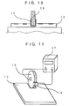
- Figs. 23 show the buffering method by which the overall sensor is covered with the gel 70.
- Fig. 23A is a top plan view
- Fig. 23B is a cross-sectional view.
- the sensor is mounted on a portion that is a supporting board of the lead frame 71, and the gel type substance is supplied by a dispenser.
- the gel 70 drips to cover the sensor.
- the gel may have viscosity so as to cover the overall sensor.
- the resin mold is obtained by injection-molding such material 120 and then packaged in Fig. 23C.
- the sensor is impact resistant because it is covered with the gel 70.
- the package used in this embodiment is of a dip type and corresponds to a regular IC package, a user can easily use this package.
- Fig. 23C shows the side view of the sensor when molded.
- Alcohol having a high flash point may be similarly used besides the silicon oil 48. As different from the oil, the alcohol can eliminate such a problem as that the peripheral portion is viscous and hard to be sealed when sealing.
- the structure in which the semiconductor substrate 11 that can be a sensor, the dead-weight 3 and the supporting body 9 are mounted on the supporting board was obtained (the acceleration sensor semiconductor device 101).
- the structure is installed in the package and a means for weaken the impact resistance is applied thereto to obtain a sensor.
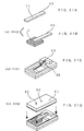
- Fig. 25 shows this embodiment.
- Two holes 81, 82 are formed to the cover to function as an oil injection hole and an exhaust hole in Fig. 25A.
- the silicon oil 48 is injected by using a dispenser 75 in Fig. 25B.
- it is preferable not to inject a full amount of the silicon oil so as to make an air bank with taking into consideration expansion of the oil due to a change in temperature.
- a means such that a sponge is set in the package to prevent the silicon oil 48 from oscillating.
- Fig. 25C shows the state where the oil is injected.
- lumps of indium 76 are used as plugs for the package in Fig. 25D.
- Indium is a material apt to be deformed and used for maintaining air tightness, it is hence excellent for sealing. Any other material can be also used if it is suitable for sealing. Sealing is achieved by putting lumps of indium on the injection hole 81 and the exhaust hole 82 and applying pressure on these lamps in Fig. 25E. The sealing method by which pressure is applied to deform the material such as indium is easy and very convenient.
- the through holes are formed on the upper portion of the package in this embodiment, through holes may be formed to the supporting board 10. Note that a narrow portion must be provided as shown in Fig. 5D to prevent the sealing material from dropping because the straight shape of the through hole involves the sealing material to fall.
- gold is provided around the holes by gold plating.
- the holes may be sealed by dropping the solder to these holes.
- ultrasonic waves may be used to achieve sealing.
- the engagement portion is heated and bonded when the ultrasonic waves are used. This method is very convenient. Note that boding can be easily made by friction heat if plastic is used to the package. Incidentally, soldering was used to achieve bonding in this embodiment.
- the package is one of most important elements for maintaining the characteristic of the present sensor.
- the characteristic When the sensor is mounted in a vehicle, the characteristic must be compensated at the temperature of not more than 125°
- This problem can be usually solved by mounting a temperature compensating circuit, but the effect can be obtained by using heat insulating material to the package in this embodiment.
- the semiconductor device having an adjustment function is provided in the vicinity of the sensor device as a device different from that having the sensor function.
- the semiconductor device having the adjustment function is called the Signal processing IC.
- the signal processing IC may includes a temperature compensating circuit, a trimming circuit for the offset adjustment or the like, an amplification circuit, a filter circuit and other circuits.
- a trimming circuit has functions of sensitivity adjustment, offset adjustment and temperature compensation. Further, another chip resistor may be used to the filter circuit.
- Figs. 26 show the trimming circuit.
- a circuit such as shown in Fig. 26B may be used.
- it is very convenient because trimming can be carried out in accordance with each resistor.
- a laser beam is used and the wire is cut to function the resistors.
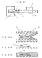
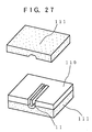
- Fig. 27 shows a regular microcomputer chip 110, and a central portion of the microcomputer chip is cut out by a cutting process such as dicing and cutting is stopped in the vicinity of the diffused resistors without performing full cut.
- the acceleration sensor in which the portion near the diffused resistors is fixed can be produced by this method.
- the diffused resistors are provided on the illustrated-top face. In this method, the microcomputer chip and the stoppers 111 are also fixed after cutting as shown in the drawing.
- the semiconductor substrate 11 is brought into contact with a wall surface and stops even if an excessive acceleration is applied, it is hence impact resistant.
- Parts other than the sensor portion were constituted by the microcomputer chip 110, and E2PROM and EPROM having the self-trimming function were used. Note that the dead-weight 3 may be provide on the side surface 100.
- the acceleration sensor Since the microcomputer chip is included, the acceleration sensor has a programmable function and is used as a programmable acceleration sensor. If temperature information and others are stored in a memory, the temperature compensation function can be established by the self-trimming function.
- setting a programmable filter (analog) in the microcomputer chip can improve the frequency characteristic without using the silicon oil.
- the acceleration sensor including the microcomputer chip can be readily manufactured.
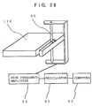
- the plasma can be used.
- a metal wire electrode 90 To a metal wire electrode 90 are connected a high frequency amplifier 91, an oscillator 92, and a computer 93.
- the plasma is produced around the metal wire electrode 90 to feed and control a piece to be machined.
- elimination reaction occurs only in the vicinity of the wire electrode, and the area to be machined is small. Further, since layers that are deformed in the machining are not generated, it is very effective.
- the plasma may be therefore used for taking out the rectangular parallelepiped type- semiconductor substrate 11 according to the present invention.
- atoms having large electronegativity such as halogen are induced in a high frequency plasma which locally exist in the high pressure atmosphere and turned to neutral radical having higher reactivity to be reacted with the piece to be machined and converted into volatile substance for elimination processing.
- the excellent machined surface can be obtained because this is a method for carrying out machining in accordance with each atom.
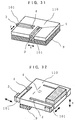
- a biaxial sensor can be realized by cutting the two-directional sensing at several positions.
- two-directional sensor can be easily produced by the above-described method utilizing the plasma.
- two-directional acceleration can be detected by machining four sides of the sensor when a microcomputer chip 110 larger than that shown in Figs. 29 and 30.
- the supporting body 9 is processed under the machined microcomputer chip as shown in the drawing so that the parts near the diffused resistors 4 are fixed and detection by the acceleration sensor device 101 is enabled.
- the dead-weight is required and may be provided at a position of the center of gravity of the acceleration sensor device 101 from the outside as shown in Figs. 29 and 30.
- the dead-weight may be provided at a tip of the acceleration sensor device 101.
- a triaxial acceleration sensor is possible when the present invention is applied.
- One side of sensor is further machined in addition to the above-described biaxial sensor, and the displacement control is performed with respect to the vertical acceleration in the drawing.
- the displacement in the Z axis in the drawing is detected. Detection of the triaxial acceleration was enabled with this configuration.
- the semiconductor device having the semiconductor acceleration sensor according to the present invention demonstrates the very excellent characteristic in impact resistance because it has the detection portion that is not thin and has no narrow part as in the prior art.
- the semiconductor device having the semiconductor acceleration sensor according to the present invention was used as an air bag operation sensor that is mounted on a vehicle to save life from collision of a vehicle, a predetermined characteristic was obtained and the device can be thus sufficiently used.
- the semiconductor acceleration sensor according to the present invention can be manufactured at a low price and has various applications. For example in case of a pager or a portable telephone, it is general to inform an incoming call using sound or inform to turn off the switch by transmitting vibration to a human body, but impact is given by tapping on the pager or the portable telephone when the semiconductor acceleration sensor according to the present invention is used.
- the semiconductor acceleration sensor detects impact to turn off the switch of the device. With such a structure, the device can be easily stopped without manually turning off the switch.
- the switch may be also turned on. For example, a desk lamp may be turned on when tapped.
- the present invention has the following advantages with the above-mentioned structure.
Landscapes
- Engineering & Computer Science (AREA)
- Microelectronics & Electronic Packaging (AREA)
- Physics & Mathematics (AREA)
- General Physics & Mathematics (AREA)
- Computer Hardware Design (AREA)
- Pressure Sensors (AREA)
Applications Claiming Priority (4)
| Application Number | Priority Date | Filing Date | Title |
|---|---|---|---|
| JP8040128A JP2800111B2 (ja) | 1996-02-27 | 1996-02-27 | 半導体装置 |
| JP40128/96 | 1996-02-27 | ||
| JP8041933A JP2800112B2 (ja) | 1996-02-28 | 1996-02-28 | 半導体装置 |
| JP41933/96 | 1996-02-28 |
Publications (2)
| Publication Number | Publication Date |
|---|---|
| EP0793103A2 true EP0793103A2 (de) | 1997-09-03 |
| EP0793103A3 EP0793103A3 (de) | 1998-10-07 |
Family
ID=26379567
Family Applications (1)
| Application Number | Title | Priority Date | Filing Date |
|---|---|---|---|
| EP97301298A Withdrawn EP0793103A3 (de) | 1996-02-27 | 1997-02-27 | Halbleiter-Beschleunigungssensor |
Country Status (1)
| Country | Link |
|---|---|
| EP (1) | EP0793103A3 (de) |
Cited By (3)
| Publication number | Priority date | Publication date | Assignee | Title |
|---|---|---|---|---|
| WO2001060736A3 (en) * | 2000-02-18 | 2002-03-21 | Motorola Inc | Methods and apparatus for a vertically-integrated sensor structure |
| US8487389B2 (en) | 2009-07-10 | 2013-07-16 | Yamaha Corporation | Uniaxial acceleration sensor |
| EP3342749A2 (de) * | 2016-12-30 | 2018-07-04 | Sonion Nederland B.V. | Mikroelektromechanischer wandler |
Family Cites Families (12)
| Publication number | Priority date | Publication date | Assignee | Title |
|---|---|---|---|---|
| EP0454190A3 (en) * | 1986-09-22 | 1992-01-08 | Nippondenso Co., Ltd. | Semiconductor accelerometer |
| JPH077012B2 (ja) * | 1987-08-18 | 1995-01-30 | 富士通株式会社 | 加速度センサ |
| EP0340476B1 (de) * | 1988-04-11 | 1993-06-16 | Nippondenso Co., Ltd. | Beschleunigungsaufnehmer |
| US5081867A (en) * | 1988-09-30 | 1992-01-21 | Nec Corporation | Semiconductor sensor |
| US4969359A (en) * | 1989-04-06 | 1990-11-13 | Ford Motor Company | Silicon accelerometer responsive to three orthogonal force components and method for fabricating |
| FR2650895B1 (fr) * | 1989-08-08 | 1991-10-11 | Onera (Off Nat Aerospatiale) | Capteur accelerometrique a poutres vibrant en flexion |
| JP2580807B2 (ja) * | 1989-11-28 | 1997-02-12 | 三菱マテリアル株式会社 | 電解ドレッシング方法および装置 |
| EP0459723B1 (de) * | 1990-05-30 | 1996-01-17 | Hitachi, Ltd. | Halbleiterbeschleunigungsmesser und Kraftfahrzeugsteuerungssystem mit einem solchen |
| US5178015A (en) * | 1991-07-22 | 1993-01-12 | Monolithic Sensors Inc. | Silicon-on-silicon differential input sensors |
| JPH07122759A (ja) * | 1993-10-27 | 1995-05-12 | Mitsubishi Electric Corp | 半導体加速度センサ |
| EP0675363A3 (de) * | 1994-03-31 | 1997-03-05 | Delco Electronics Corp | Beschleunigungsmessanordnung. |
| JP3114006B2 (ja) * | 1994-08-29 | 2000-12-04 | セイコーインスツルメンツ株式会社 | 半導体装置、及び、その製造方法 |
-
1997
- 1997-02-27 EP EP97301298A patent/EP0793103A3/de not_active Withdrawn
Cited By (5)
| Publication number | Priority date | Publication date | Assignee | Title |
|---|---|---|---|---|
| WO2001060736A3 (en) * | 2000-02-18 | 2002-03-21 | Motorola Inc | Methods and apparatus for a vertically-integrated sensor structure |
| US8487389B2 (en) | 2009-07-10 | 2013-07-16 | Yamaha Corporation | Uniaxial acceleration sensor |
| EP3342749A2 (de) * | 2016-12-30 | 2018-07-04 | Sonion Nederland B.V. | Mikroelektromechanischer wandler |
| US11358859B2 (en) | 2016-12-30 | 2022-06-14 | Sonion Nederland B.V. | Micro-electromechanical transducer |
| US11760624B2 (en) | 2016-12-30 | 2023-09-19 | Sonion Nederland B.V. | Micro-electromechanical transducer |
Also Published As
| Publication number | Publication date |
|---|---|
| EP0793103A3 (de) | 1998-10-07 |
Similar Documents
| Publication | Publication Date | Title |
|---|---|---|
| US6158283A (en) | Semiconductor acceleration sensor | |
| US5559290A (en) | Capacitance type accelerometer | |
| US6405592B1 (en) | Hermetically-sealed sensor with a movable microstructure | |
| US6391742B2 (en) | Small size electronic part and a method for manufacturing the same, and a method for forming a via hole for use in the same | |
| US6848306B2 (en) | Semiconductor dynamic sensor | |
| JP2009241164A (ja) | 半導体センサー装置およびその製造方法 | |
| US5828116A (en) | Semiconductor device with bonded wires | |
| US5535626A (en) | Sensor having direct-mounted sensing element | |
| US5608153A (en) | Semiconductor acceleration sensor and testing method thereof | |
| JP5052459B2 (ja) | 半導体センサー装置 | |
| JP2728237B2 (ja) | 静電容量式加速度センサ | |
| US20040263186A1 (en) | Capacitance type dynamic quantity sensor | |
| US11659664B2 (en) | Electronic device | |
| EP0793103A2 (de) | Halbleiter-Beschleunigungssensor | |
| US6006606A (en) | Semiconductor acceleration sensor | |
| US7037805B2 (en) | Methods and apparatus for attaching a die to a substrate | |
| JP2800111B2 (ja) | 半導体装置 | |
| JP2001311675A (ja) | 圧力センサモジュール | |
| JP2018132311A (ja) | 物理量検出装置および電子機器 | |
| JPH0447271A (ja) | 加速度センサ及びその出力電圧調整方法 | |
| US20250172393A1 (en) | Vibrator Device And Method For Manufacturing Vibrator Device | |
| JPH0926371A (ja) | 半導体式圧力センサ | |
| JPH10209469A (ja) | 半導体圧力センサ | |
| US12584741B2 (en) | Inertial measurement device and method for manufacturing inertial measurement device | |
| US20250155466A1 (en) | Method For Manufacturing Electronic Device |
Legal Events
| Date | Code | Title | Description |
|---|---|---|---|
| PUAI | Public reference made under article 153(3) epc to a published international application that has entered the european phase |
Free format text: ORIGINAL CODE: 0009012 |
|
| AK | Designated contracting states |
Kind code of ref document: A2 Designated state(s): DE FR IT |
|
| PUAL | Search report despatched |
Free format text: ORIGINAL CODE: 0009013 |
|
| AK | Designated contracting states |
Kind code of ref document: A3 Designated state(s): DE FR IT |
|
| STAA | Information on the status of an ep patent application or granted ep patent |
Free format text: STATUS: THE APPLICATION IS DEEMED TO BE WITHDRAWN |
|
| 18D | Application deemed to be withdrawn |
Effective date: 19990408 |