EP0793267A2 - Verbesserte Maskierungsverfahren bei der Herstellung einer Halbleiteranordnung - Google Patents
Verbesserte Maskierungsverfahren bei der Herstellung einer Halbleiteranordnung Download PDFInfo
- Publication number
- EP0793267A2 EP0793267A2 EP97102587A EP97102587A EP0793267A2 EP 0793267 A2 EP0793267 A2 EP 0793267A2 EP 97102587 A EP97102587 A EP 97102587A EP 97102587 A EP97102587 A EP 97102587A EP 0793267 A2 EP0793267 A2 EP 0793267A2
- Authority
- EP
- European Patent Office
- Prior art keywords
- mask
- semiconductor devices
- substrate
- during fabrication
- surfaces during
- Prior art date
- Legal status (The legal status is an assumption and is not a legal conclusion. Google has not performed a legal analysis and makes no representation as to the accuracy of the status listed.)
- Withdrawn
Links
Images
Classifications
-
- H—ELECTRICITY
- H10—SEMICONDUCTOR DEVICES; ELECTRIC SOLID-STATE DEVICES NOT OTHERWISE PROVIDED FOR
- H10P—GENERIC PROCESSES OR APPARATUS FOR THE MANUFACTURE OR TREATMENT OF DEVICES COVERED BY CLASS H10
- H10P50/00—Etching of wafers, substrates or parts of devices
- H10P50/69—Etching of wafers, substrates or parts of devices using masks for semiconductor materials
- H10P50/691—Etching of wafers, substrates or parts of devices using masks for semiconductor materials for Group V materials or Group III-V materials
- H10P50/693—Etching of wafers, substrates or parts of devices using masks for semiconductor materials for Group V materials or Group III-V materials characterised by their size, orientation, disposition, behaviour or shape, in horizontal or vertical plane
- H10P50/695—Etching of wafers, substrates or parts of devices using masks for semiconductor materials for Group V materials or Group III-V materials characterised by their size, orientation, disposition, behaviour or shape, in horizontal or vertical plane characterised by the process involved to create the mask, e.g. lift-off masks or sidewalls or to modify the mask
Definitions
- the present invention pertains to the fabrication of semiconductor devices and more specifically to improved masking techniques during semiconductor device fabrication.
- masking material e.g. nitride/oxide or the like
- semiconductor material is grown over masked and unmasked areas.
- the material on the masked areas is then removed by etching and lift-off.
- material is selectively grown in unmasked areas and the masking material is then removed.
- a photoresist mask is used to define and develop a hard mask, i.e. a metal mask, a nitride mask, etc.
- etching is required to remove unwanted material and masks are removed by etching, solvent, or the like.
- the material of the semiconductor device has a high likelihood of being contaminated by the etchant, which contamination greatly reduces the life of the device, the operating characteristics of the device, and the reliability of the device.
- the etching process severely damages semiconductor material adjacent the etched areas which further reduces life, operating characteristics, and reliability.
- etching processes are very time consuming and difficult to perform.
- the above problems and others are at least partially solved and the above purposes and others are realized in a method of masking surfaces during fabrication of semiconductor devices which includes providing a gallium arsenide substrate, or other III-V compounds, with or without a layer of native oxide thereon.
- a metal mask is positioned on the surface so as to define a growth area and an unmasked portion on the surface.
- Ultraviolet light is directed at the unmasked area, by exposing the surface to a bright light, so as to grow an oxide film on the unmasked portion of the surface.
- the metal mask is removed and the oxide film then serves as a mask for further operations and can be easily removed in situ by heating or dry etching. If native oxide is included, it can be removed in situ by heating the substrate to a lower temperature than is required to desorb the oxide mask.
- the mask positioned on the surface is a hard mask, such as a chrome mask or the like.
- a bright light is used, such as that present in an aligner or stepper, which bright light preferably includes deep ultraviolet light.
- the substrate is then introduced into a growth chamber and may be heated to a first temperature to desorb any native oxide that is present.
- a crystalline material is selectively grown on the exposed growth area and the substrate is heated to a second higher temperature to desorb the oxide layer in the growth chamber.
- semiconductor devices are grown and the mask is removed without taking the substrate from the growth chamber.
- the oxide layer can be used as an etch mask or for any other semiconductor processes that require masking.
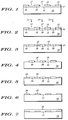
- FIGS. 1 - 4 illustrate several steps in a method of masking a gallium arsenide substrate 10, in accordance with the present invention, for the fabrication of semiconductor devices.
- gallium arsenide substrate 10 is utilized herein for purposes of this description but other III-V compounds and other semiconductor materials may be utilized in other applications.
- FIG. 1 a simplified sectional view of gallium arsenide substrate 10 having a surface 11 is illustrated.
- substrate 10 might simply be a supporting structure, such as a wafer or the like, or it might include various layers formed on or in the supporting structure.
- Surface 11 of gallium arsenide substrate 10 has a film 12 (generally 20 angstroms or less) of a native oxide which, as is well known in the art, forms generally instantaneously upon exposure to air.
- a native oxide is not always necessary to the present invention and is only illustrated because it is generally present and requires special procedures to prevent.
- various types of passivation may be used, to prevent the formation of film 12, in which case such passivation may have to be removed before the present procedure can be performed. It has been found that the present technique will operate generally as described with the surface simply being clean (i.e. no foreign matter).
- a mask 15 is positioned adjacent to surface 11 of substrate 10 for patterning surface 11, as will be explained presently.
- Mask 15 generally is a shadow or metal mask but, in some special applications, it can be formed in the well known manner with photolithography as in an aligner or stepper (generally includes a projected image from a mask). As will become apparent presently, one of the major advantages of the present technique is that photolithography and the like are not necessary for the described masking operations.
- mask 15 is a mask plate with metal lines and other features, for example, a chrome mask. In any case, mask 15 is positioned adjacent surface 11 so as to define one or more growth areas 16 on surface 11 beneath mask 15 and one or more unmasked portions 17 on surface 11 of substrate 10.
- Unmasked portions 17 of surface 11 are exposed to a bright light preferably including deep ultraviolet, represented by arrows 21 in FIG. 2.
- the bright light may be, for example, the type typically used in aligners, steppers, or E-beam devices in the semiconductor industry.
- the term "deep ultraviolet” refers to light in the ultraviolet range, generally with a wavelength in the range of 180 to 250 nanometers. In the present specific example, it is believed that the 185 nm light generates ozone due to optical excitation. Therefore, excitation wavelength that is most suitable for efficient ozone generation is also the most efficient to use, although virtually any ultraviolet light will produce the desired result.
- exposure to other wavelenghts modifies the composition of the surface oxide by forming a different kind of oxide or complex oxide molecules that are more stable than the native oxide.
- the exposure to light can be performed under a lamp.
- sharp features can be defined in unmasked portion 17.
- a gallium arsenide wafer with a layer of native oxide on the surface was provided.
- oxide film 20 is grown, mask 15 is removed to expose growth areas 16, as illustrated in FIG. 3.
- Oxide film 20 then serves as a mask for further process operations, such as growth, etching, and so on, and can be easily removed in situ by heating, if necessary.
- substrate 10 is then introduced into a growth chamber (not shown) and heated to a temperature of approximately 580°C to desorb any native oxide that may still be present in growth areas 16.
- substrate 10 with native oxide-free growth areas 16 is illustrated in FIG. 4.
- selective growth of crystalline, or semiconductor, material 25 in growth areas 16 is performed, as illustrated in FIG. 5.
- oxide film 20 in place as a mask for further growth, a predetermined amount of crystalline material 25 is selectively grown in area (or areas) 16.
- selective growth or “selectively grown” is defined as growing only in the specific or designated area.
- selective InAs was selectively grown using trimethyl indium and arsine in a chemical beam epitaxy.
- material 25 grows only in growth areas 16.
- material 25 generally grows in a crystalline form so that growth rates and shapes are crystallographic dependent, i.e. the rate and shape of growth are dependent upon the type of material 25 being utilized.
- substrate 10 is heated to a higher temperature (approximately, 640°C) in the growth chamber to desorb oxide film 20, resulting in the structure illustrated in FIG. 6.
- a higher temperature approximately, 640°C
- the mask utilized for patterned growth of material 25 is desorbed, or removed, in situ, i.e. without the need to remove substrate 10 from the growth chamber.
- oxide film 20 can be incorporated into and retained as a portion of some types of semiconductor devices.
- oxide film 20 can be used as a gate oxide in some insulated gate field effect transistors. In which case oxide film 20 is grown as described above and is then masked to define the gate area, after which a metal layer is formed thereon to define the gate electrode.
- an improved masking processes which provides a new and improved method of masking gallium arsenide substrates during semiconductor device fabrication.
- the new and improved method of masking gallium arsenide substrates includes a simplified method of masking silicon without requiring photoresists, nitride/oxide, and the like.
- the absence of resist in the process improves resolution limits previously defined by resist thickness.
- the new process eliminates a number of process steps and, hence, is cheaper, cleaner, improves yield, can result in better resolution and therefore smaller lines, and makes the fabrication process vacuum compatible.
- the oxide layer can be used as an etch mask or for any other semiconductor processes that require masking.
- the new and improved method of masking gallium arsenide substrates does not require the introduction and removal of wafers or substrates from processing chambers several times in sequence during the fabrication of semiconductor devices, the fabrication process is much simpler and includes less chance of contamination of the devices.
- the present novel process allows selective growth and further re-growth, all in-situ, without exposure to air and contamination during the intermediate processing steps between epitaxy, etc. By eliminating air and other contaminant exposure between steps, the novel process ensures good quality in subsequent epitaxial steps
Landscapes
- Formation Of Insulating Films (AREA)
- Local Oxidation Of Silicon (AREA)
Applications Claiming Priority (2)
| Application Number | Priority Date | Filing Date | Title |
|---|---|---|---|
| US08/609,704 US5709744A (en) | 1996-03-01 | 1996-03-01 | Masking methods during semiconductor device fabrication |
| US609704 | 1996-03-01 |
Publications (2)
| Publication Number | Publication Date |
|---|---|
| EP0793267A2 true EP0793267A2 (de) | 1997-09-03 |
| EP0793267A3 EP0793267A3 (de) | 1997-11-12 |
Family
ID=24441971
Family Applications (1)
| Application Number | Title | Priority Date | Filing Date |
|---|---|---|---|
| EP97102587A Withdrawn EP0793267A3 (de) | 1996-03-01 | 1997-02-17 | Verbesserte Maskierungsverfahren bei der Herstellung einer Halbleiteranordnung |
Country Status (3)
| Country | Link |
|---|---|
| US (1) | US5709744A (de) |
| EP (1) | EP0793267A3 (de) |
| JP (1) | JPH09246266A (de) |
Citations (1)
| Publication number | Priority date | Publication date | Assignee | Title |
|---|---|---|---|---|
| EP0657924A2 (de) * | 1993-12-09 | 1995-06-14 | Kabushiki Kaisha Toshiba | Methode zur Analyse von Oberflächen verunreinigungen auf Halbleitersubstraten |
Family Cites Families (3)
| Publication number | Priority date | Publication date | Assignee | Title |
|---|---|---|---|---|
| US4717681A (en) * | 1986-05-19 | 1988-01-05 | Texas Instruments Incorporated | Method of making a heterojunction bipolar transistor with SIPOS |
| US4994140A (en) * | 1989-01-10 | 1991-02-19 | Optoelectronics Technology Research Corporation | Method capable of forming a fine pattern without crystal defects |
| US5730798A (en) * | 1995-08-07 | 1998-03-24 | Motorola | Masking methods during semiconductor device fabrication |
-
1996
- 1996-03-01 US US08/609,704 patent/US5709744A/en not_active Expired - Lifetime
-
1997
- 1997-02-17 EP EP97102587A patent/EP0793267A3/de not_active Withdrawn
- 1997-02-26 JP JP9059789A patent/JPH09246266A/ja active Pending
Patent Citations (1)
| Publication number | Priority date | Publication date | Assignee | Title |
|---|---|---|---|---|
| EP0657924A2 (de) * | 1993-12-09 | 1995-06-14 | Kabushiki Kaisha Toshiba | Methode zur Analyse von Oberflächen verunreinigungen auf Halbleitersubstraten |
Also Published As
| Publication number | Publication date |
|---|---|
| US5709744A (en) | 1998-01-20 |
| EP0793267A3 (de) | 1997-11-12 |
| JPH09246266A (ja) | 1997-09-19 |
Similar Documents
| Publication | Publication Date | Title |
|---|---|---|
| US5700703A (en) | Method of fabricating buried control elements in semiconductor devices | |
| US4637129A (en) | Selective area III-V growth and lift-off using tungsten patterning | |
| US4994140A (en) | Method capable of forming a fine pattern without crystal defects | |
| JPH0734428B2 (ja) | 半導体素子の製造方法 | |
| EP0758143B1 (de) | Verbesserte Maskierungsverfahren während der Herstellung einer Halbleiteranordnung | |
| US5904552A (en) | Method of resistless patterning of a substrate for implantation | |
| EP0783176B1 (de) | Verbesserte Maskierungsverfahren bei der Halbleiterproduktion | |
| JPH0543287B2 (de) | ||
| US5877071A (en) | Masking methods during semiconductor device fabrication | |
| US5709744A (en) | Masking methods during semiconductor device fabrication | |
| US5830801A (en) | Resistless methods of gate formation in MOS devices | |
| JP2003520432A (ja) | シリサイド形成のための半導体基板の製造方法 | |
| US5837560A (en) | Method of masking substrates leaving exposed facets | |
| US5897366A (en) | Method of resistless gate metal etch for fets | |
| US4680087A (en) | Etching of dielectric layers with electrons in the presence of sulfur hexafluoride | |
| US20040067627A1 (en) | Dry lithograpy method and method of forming gate pattern using the same | |
| JP2500443B2 (ja) | 化合物半導体のドライエッチング方法 | |
| JP3080860B2 (ja) | ドライエッチング方法 | |
| US6481119B1 (en) | Apparatus for removing organic antireflection coating | |
| JPH01316926A (ja) | 半導体薄膜結晶の製造方法 | |
| JPH05109702A (ja) | 半導体装置の製造方法 | |
| US6001722A (en) | Selective metallization/deposition for semiconductor devices | |
| US6291135B1 (en) | Ionization technique to reduce defects on next generation lithography mask during exposure | |
| US5733817A (en) | Blanket oxidation for contact isolation | |
| JP2717165B2 (ja) | 化合物半導体の構造形成方法 |
Legal Events
| Date | Code | Title | Description |
|---|---|---|---|
| PUAI | Public reference made under article 153(3) epc to a published international application that has entered the european phase |
Free format text: ORIGINAL CODE: 0009012 |
|
| AK | Designated contracting states |
Kind code of ref document: A2 Designated state(s): DE GB |
|
| PUAL | Search report despatched |
Free format text: ORIGINAL CODE: 0009013 |
|
| RHK1 | Main classification (correction) |
Ipc: H01L 21/316 |
|
| AK | Designated contracting states |
Kind code of ref document: A3 Designated state(s): DE GB |
|
| 17P | Request for examination filed |
Effective date: 19980512 |
|
| 17Q | First examination report despatched |
Effective date: 20010201 |
|
| GRAP | Despatch of communication of intention to grant a patent |
Free format text: ORIGINAL CODE: EPIDOSNIGR1 |
|
| GRAJ | Information related to disapproval of communication of intention to grant by the applicant or resumption of examination proceedings by the epo deleted |
Free format text: ORIGINAL CODE: EPIDOSDIGR1 |
|
| GRAP | Despatch of communication of intention to grant a patent |
Free format text: ORIGINAL CODE: EPIDOSNIGR1 |
|
| STAA | Information on the status of an ep patent application or granted ep patent |
Free format text: STATUS: THE APPLICATION IS DEEMED TO BE WITHDRAWN |
|
| 18D | Application deemed to be withdrawn |
Effective date: 20040210 |