EP0793354A2 - Integrierte Struktur eines Viterbi-Faltungsdekoders - Google Patents
Integrierte Struktur eines Viterbi-Faltungsdekoders Download PDFInfo
- Publication number
- EP0793354A2 EP0793354A2 EP97410024A EP97410024A EP0793354A2 EP 0793354 A2 EP0793354 A2 EP 0793354A2 EP 97410024 A EP97410024 A EP 97410024A EP 97410024 A EP97410024 A EP 97410024A EP 0793354 A2 EP0793354 A2 EP 0793354A2
- Authority
- EP
- European Patent Office
- Prior art keywords
- modules
- state
- acs
- module
- pair
- Prior art date
- Legal status (The legal status is an assumption and is not a legal conclusion. Google has not performed a legal analysis and makes no representation as to the accuracy of the status listed.)
- Granted
Links
Images


Classifications
-
- H—ELECTRICITY
- H03—ELECTRONIC CIRCUITRY
- H03M—CODING; DECODING; CODE CONVERSION IN GENERAL
- H03M13/00—Coding, decoding or code conversion, for error detection or error correction; Coding theory basic assumptions; Coding bounds; Error probability evaluation methods; Channel models; Simulation or testing of codes
- H03M13/65—Purpose and implementation aspects
- H03M13/6502—Reduction of hardware complexity or efficient processing
-
- H—ELECTRICITY
- H03—ELECTRONIC CIRCUITRY
- H03M—CODING; DECODING; CODE CONVERSION IN GENERAL
- H03M13/00—Coding, decoding or code conversion, for error detection or error correction; Coding theory basic assumptions; Coding bounds; Error probability evaluation methods; Channel models; Simulation or testing of codes
- H03M13/37—Decoding methods or techniques, not specific to the particular type of coding provided for in groups H03M13/03 - H03M13/35
- H03M13/39—Sequence estimation, i.e. using statistical methods for the reconstruction of the original codes
- H03M13/41—Sequence estimation, i.e. using statistical methods for the reconstruction of the original codes using the Viterbi algorithm or Viterbi processors
- H03M13/4107—Sequence estimation, i.e. using statistical methods for the reconstruction of the original codes using the Viterbi algorithm or Viterbi processors implementing add, compare, select [ACS] operations
Definitions
- the present invention relates to an integrated circuit structure of a Viterbi convolutional decoder, and more particularly to the integrated structure of the add-comparison-selection modules of the decoder.
- Convolutional coding and decoding are used to decrease errors in digital signal transmissions.
- an addition-comparison-selection (ACS) module is associated with each node of what is called a trellis.
- Each node of the trellis corresponds to a possible state of a shift register used in convolutional coding.
- Figure 1 illustrates a generic trellis used to construct any trellis with N states.
- a 2n state and a 2n + 1 state are both linked to an n state and to an n + N / 2 state.
- the number n is any positive integer and the numbers 2n and 2n + 1 are defined modulo-N.
- the links between states correspond to transitions determined by symbols received by the decoder. In this example, each symbol contains two bits of information.
- the transitions from state n to state 2n and from state n + N / 2 to state 2n + 1 correspond to the reception of a symbol ab, where a is equal to 1 or 0 and b is equal to 1 or 0 depending on the value of 2n.
- the transitions from state n to state 2n + 1 and from state n + N / 2 to state 2n correspond to the reception of the symbol ab ⁇ .
- FIG. 2 represents essential elements of the ACS module associated with state 2n.
- This ACS module (2n) is intended to update an associated path metric PM (2n) in a register 10 and to provide a decision D (2n).
- Each path metric is a 7-bit number, for example.
- the ACS module (2n) comprises an adder 12 which receives the path metric PM (n) from the ACS module associated with the state n and a connection metric BMab associated, in the present example, with the symbol ab.
- a second adder 13 receives the path metric PM (n + N / 2) supplied by the ACS module associated with the state n + N / 2 and a connection metric BM ab ⁇ associated, in this example, with the symbol ab ⁇ .
- a BMx branching metric is a number of five bits, for example, which is all the lower the greater the probability of having received the corresponding symbol x.
- PM path metric
- the decision D (2n) is provided by a comparator 15 receiving the outputs of the adders 12 and 13. It controls a multiplexer 17 in order to select, among the outputs of the adders 12 and 13, the one whose value is the lowest. Thus, the decision D (2n) indicates the most probable previous state among the states n and n + N / 2.
- the output of the multiplexer 17 is stored in the register 10 as a path metric PM (2n) to be used on reception of the following symbol.
- the ACS module associated with the state 2n + 1 is similar to that of FIG. 2, except that the adder 12 receives the BM connection metric ab ⁇ and the adder 13 receives the connection metric BMab.
- the trellis is relatively large, for example 64 states. Then, the interconnections between ACS modules become complex and it is necessary to pay particular care to the placement and routing of these ACS modules on an integrated circuit, in order not to occupy a considerable surface and affect the speed of operation.
- FIG. 3 is intended to illustrate the general principle of placement and routing of Sparso.
- the ACS modules are grouped in pairs into two columns separated by a common routing channel 20. Each pair comprises, juxtaposed in the direction of the width of the corresponding column, the modules associated with the states 2n and 2n + 1 (modulo-N, n being any). These two ACS modules receive the path metric PM provided by the ACS module associated with the n state or with the n + N / 2 state which is, as shown, in a previous close torque, on the far side of the common channel 20. The missing path metric arrives at the ACS modules associated with states 2n and 2n + 1 via common channel 20.
- FIG. 4 schematically illustrates a network structure of ACS modules, obtained using the Sparso method in the example of a 64-state trellis.
- the ACS modules are illustrated by boxes designated by the associated states.
- the Sparso method is optimal when using integration technologies with two layers of metallizations. In more recent technologies, three layers of metallization are available. If we transpose the Sparso method to a technology with three layers of metallization, we do not succeed in significantly reducing the size of the network of ACS modules compared to the same network produced in a technology with two layers of metallization.
- An object of the present invention is to provide an optimal integrated structure of a network of ACS modules in a technology with three layers of metallizations.
- ACS addition-comparison-selection
- the ACS modules are physically grouped in pairs juxtaposed to form two separate parallel columns, each pair comprising two modules associated respectively with states 2n and 2n + 1 modulo-N, and each of which is connected, to receive two path metrics, to the module associated with one of states n and n + N / 2 of a close pair and with the module associated with the other of the states n and n + N / 2 of a distant couple, the space between the two columns constituting a common channel comprising the links between modules of distant couples.
- the structure is made in a three-layer metallization technology and the two ACS modules of each pair are juxtaposed in the height direction of the columns.
- each ACS module of a pair is connected to two among four groups of lines of supply of connection metrics, common to each column.
- each ACS module comprises first to third groups of pads for establishing the connections with the following close torque respectively and the modules associated with states n and n + N / 2, and of the fourth and fifth groups of pads for establishing connections with the two corresponding groups of lines respectively, all the pads being arranged according to a topology common to all the modules.
- the pads of each group of pads are distributed over the width of the corresponding column, the pads associated with most significant bits being on the side remote from the common channel, where a common circuit is integrated to the two modules of the corresponding torque.
- the present invention aims to integrate the addition-comparison-selection (ACS) modules of a Viterbi convolutional decoder optimally in a technology with three layers of metallizations.
- the invention is partially based on the structure of Sparso ( Figures 3 and 4). Sparso's structure is optimal for integration technologies with two layers of metallization. However, by transposing this structure into a technology with three layers of metallization, it turns out that the occupied surface cannot be reduced significantly. In particular, it is not possible to avoid the local routing channels 22 separating the pairs of ACS modules in each column.
- pairs of ACS modules are used which are determined by the Sparso method, but the ACS modules of each pair, instead of being juxtaposed in the direction of the width of the columns, are juxtaposed in the direction of the height .
- Each ACS module is therefore distributed over the width of the corresponding column.
- the connections between the ACS modules of the same torque are very short and vertical. This frees up space for horizontal connections and it is used for connections from ACS modules to path metrics PM of the common channel 20. It is practically possible to delete the local routing channels 22.
- the surface occupied by a network of ACS modules according to the invention is approximately three times less than that of the Sparso structure.
- the reduction in surface area also has the advantage of causing an increase in the operating limit frequency.
- the first ACS module of a pair according to the invention corresponds to a module on the far side of the common channel in the Sparso structure.
- the ACS modules have the same topology.
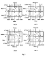
- the invention provides four configurations of pairs of ACS modules which, by juxtaposing them to form a column, establish virtually all of the internal connections to the column.
- a column is formed by choosing the configurations as a function of the couples to be obtained, it practically remains to route only the connections external to the column, in particular those between distant couples which pass through the common channel.
- Each ACS module associated with the state 2n or 2n + 1 of the trellis includes a pad 50 for providing path metric PM; a pad 51 for receiving the path metric PM (n) coming from the module associated with the state n; a pad 52 for receiving the path metric PM (n + N / 2) coming from the module associated with the state n + N / 2; and two pads 53 and 54 to receive respectively the two corresponding BM connection metrics among the four possible connection metrics.
- connection metrics BM00, BM01, BM10, and BM11 are distributed to all the modules of a column by lines extending over the height of the column.
- the connections of the pads 53 and 54 to the connection metric lines are made by vertical lines going up to the outside of the pairs of modules where, in reduced local routing channels, they join the corresponding BM lines horizontally. This is shown for configurations 0 and 1 in which, by way of example, the pads 53 and 54 of the ACS module (2n) respectively receive the metrics BM00 and BM11 and pads 53 and 54 of the ACS module (2n + 1) receive the metrics BM11 and BM00 respectively.
- Each PM path or BM connection metric is a number of several bits to which we associate, in fact, a group of plots which are scattered across the width of the column.
- connections that must be established in the local routing channels is such that the surface occupied by these local channels is negligible (approximately 5% against approximately 30% in the architecture of Sparso).
- the topologies of the ACS modules are identical and the internal assignments of pads 50 to 54 cannot be modified.
- the four configurations are distinguished by the metallizations which connect the studs 50 to 54 to the outside.
- Metallizations are only shown for connections which vary from one configuration to another.
- the modules include other pads, intended in particular to receive supply voltages and control and clock signals.
- the corresponding metallizations, not shown, are the same for the four configurations, and they are provided so that they connect properly by the juxtaposition of the couples.
- the ACS module associated with state 2n is the one which supplies the path metric PM (2n) to the next close torque.
- the two torque modules receive the metric PM (n) of the previous close torque.
- the PM path metric (2n + 1) is supplied to the common channel and the PM path metric (n + N / 2) is received by the common channel.
- the ACS modules are inverted with respect to configuration 0, that is to say that it is the module associated with the state 2n + 1 which provides the path metric PM (2n + 1) to the next close couple.
- configuration 0 is the external assignment of pads 50 to 54 which differentiates the way in which the pair of modules is routed with the outside, as is shown for connections to BM00 and BM11 connection metrics.
- the module associated with state 2n supplies its path metric PM (2n) to the next close pair, and the two modules receive from the close pair preceding the path metric PM (n + N / 2).
- the PM path metric (2n + 1) is supplied to the common channel and the PM path metric (n) is received by the common channel.
- the ACS modules are inverted with respect to configuration 2, that is to say that the module associated with the state 2n + 1 supplies its path metric PM (2n + 1) to the next close torque .
- the only difference with configuration 2 lies in the external assignment of pads 50 to 54.
- the links which are not made by juxtaposition are routed automatically, in particular the links of the common channel 20 and the links to the metric branch lines by the reduced local channels.
- An advantage of the present invention is that certain circuits can, without constraints, be put in common with two modules of each couple. This is particularly the case for a normalization circuit which is intended to control the overflow of the path metric registers 10. These common circuits are located on the side of the most significant bits of the ACS modules, that is to say on the exterior side of the circuit, the least significant bits being located on the side of the central channel 20. This minimizes the length of the links between distant modules, and therefore increases the speed of the circuit.
- a shared normalization circuit should be placed between the two modules of a couple.
- the two modules would then be of symmetrical topologies, since the most significant bits should be on the side of the central normalization circuit. This symmetry would cause an imbalance in length between the least significant lines on the side of the common channel and the least significant lines on the opposite side. This imbalance would cause a decrease in the operating frequency.
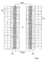
- FIG. 6 schematically illustrates an integrated structure obtained according to the invention from a network of ACS modules in the example of a 64-state trellis.
- the number of the configuration used for each pair is indicated in a box 60 next to each pair, this box representing the circuits common to the two modules of the pair.
Landscapes
- Physics & Mathematics (AREA)
- Probability & Statistics with Applications (AREA)
- Engineering & Computer Science (AREA)
- Theoretical Computer Science (AREA)
- Error Detection And Correction (AREA)
- Detection And Correction Of Errors (AREA)
Applications Claiming Priority (2)
| Application Number | Priority Date | Filing Date | Title |
|---|---|---|---|
| FR9602647A FR2745448B1 (fr) | 1996-02-28 | 1996-02-28 | Structure integree d'un decodeur convolutif de viterbi |
| FR9602647 | 1996-02-28 |
Publications (3)
| Publication Number | Publication Date |
|---|---|
| EP0793354A2 true EP0793354A2 (de) | 1997-09-03 |
| EP0793354A3 EP0793354A3 (de) | 1999-11-10 |
| EP0793354B1 EP0793354B1 (de) | 2003-04-16 |
Family
ID=9489788
Family Applications (1)
| Application Number | Title | Priority Date | Filing Date |
|---|---|---|---|
| EP97410024A Expired - Lifetime EP0793354B1 (de) | 1996-02-28 | 1997-02-25 | Integrierte Struktur eines Viterbi-Faltungsdekoders |
Country Status (5)
| Country | Link |
|---|---|
| US (1) | US5964897A (de) |
| EP (1) | EP0793354B1 (de) |
| JP (1) | JPH1051321A (de) |
| DE (1) | DE69720834D1 (de) |
| FR (1) | FR2745448B1 (de) |
Families Citing this family (2)
| Publication number | Priority date | Publication date | Assignee | Title |
|---|---|---|---|---|
| EP0851591B1 (de) * | 1996-12-24 | 2001-09-12 | Matsushita Electric Industrial Co., Ltd. | Datenprozessor und Verfahren zur Datenverarbeitung |
| CN120185624B (zh) * | 2025-05-21 | 2025-08-05 | 成都中科比智科技有限公司 | 一种高速并行维特比译码方法及系统 |
Family Cites Families (5)
| Publication number | Priority date | Publication date | Assignee | Title |
|---|---|---|---|---|
| US4924492A (en) * | 1988-03-22 | 1990-05-08 | American Telephone And Telegraph Company | Method and apparatus for wideband transmission of digital signals between, for example, a telephone central office and customer premises |
| US5068859A (en) * | 1989-06-19 | 1991-11-26 | California Institute Of Technology | Large constraint length high speed viterbi decoder based on a modular hierarchial decomposition of the deBruijn graph |
| US5134690A (en) * | 1989-06-26 | 1992-07-28 | Samatham Maheswara R | Augumented multiprocessor networks |
| US5491705A (en) * | 1992-06-18 | 1996-02-13 | The United States Of America As Represented By The Secretary Of The Air Force | De bruijn graph based VLSI viterbi decoder |
| US5390198A (en) * | 1993-05-26 | 1995-02-14 | The Boeing Company | Soft decision viterbi decoder for M-ary convolutional codes |
-
1996
- 1996-02-28 FR FR9602647A patent/FR2745448B1/fr not_active Expired - Fee Related
-
1997
- 1997-02-18 US US08/801,479 patent/US5964897A/en not_active Expired - Lifetime
- 1997-02-25 DE DE69720834T patent/DE69720834D1/de not_active Expired - Lifetime
- 1997-02-25 EP EP97410024A patent/EP0793354B1/de not_active Expired - Lifetime
- 1997-02-28 JP JP9060179A patent/JPH1051321A/ja not_active Withdrawn
Also Published As
| Publication number | Publication date |
|---|---|
| EP0793354B1 (de) | 2003-04-16 |
| FR2745448B1 (fr) | 1998-05-15 |
| US5964897A (en) | 1999-10-12 |
| EP0793354A3 (de) | 1999-11-10 |
| JPH1051321A (ja) | 1998-02-20 |
| DE69720834D1 (de) | 2003-05-22 |
| FR2745448A1 (fr) | 1997-08-29 |
Similar Documents
| Publication | Publication Date | Title |
|---|---|---|
| FR2550012A1 (fr) | Dispositif a circuits integres a semi-conducteurs | |
| FR2718571A1 (fr) | Composant hybride semiconducteur. | |
| EP0143039A1 (de) | Herstellungsverfahren einer Anordnung elektronischer Bauteile | |
| EP0553050B1 (de) | Verfahren zur Maximalwahrscheinlichkeitsdekodierung mit unterabgetastetem Dekodierungstrellis und entsprechende Dekodierungsvorrichtung | |
| EP0616479B1 (de) | Verfahren zur Neukonfigurierung eines Maschennetzwerks | |
| EP0090704B1 (de) | Vordiffundierter integrierter Schaltkreis und Verfahren zum Zwischenverbinden der Zellen dieses Schaltkreises | |
| EP1368895A1 (de) | Oberflächenwellenfilter | |
| EP0793354B1 (de) | Integrierte Struktur eines Viterbi-Faltungsdekoders | |
| FR2812988A1 (fr) | Commutateur de signaux optiques | |
| FR3071932A1 (fr) | Commutateurs et reseau d'interconnexion photonique integre dans une puce optoelectronique | |
| EP1499054A2 (de) | Verfahren zur Bestimmung des spektralen Weges in einem optischen Telekommunikationsnetzwerk | |
| EP2363813B1 (de) | Chip und integrierte Schaltung mit einem solchen Chip | |
| FR2735620A1 (fr) | Reseau de commutateurs pour la connexion de canaux redondants | |
| FR2933826A1 (fr) | Reseau logique programmable, commutateur d'interconnexion et unite logique pour un tel reseau | |
| EP0905766A1 (de) | Struktur und Verfahren zum Reparieren einer integrierten Schaltung | |
| EP2647217B1 (de) | Netzwerk aus schaltern und ladung eines telekommunikationssatelliten mit einem netzwerk aus schaltern | |
| EP0341097A1 (de) | Rekursiver Addierer zur Berechnung der Summe zweier Operanden | |
| FR2808148A1 (fr) | Matrice de commutateurs comportant des entrees et des sorties en exces | |
| EP0690636A1 (de) | Erweiterbare Vermittlungsanordnung um ein die Anordnung benutzendes System | |
| FR3074385A1 (fr) | Commutateurs et reseau d'interconnexion photonique integre dans une puce optoelectronique | |
| WO1997001251A1 (fr) | Reseau de commutateurs c pour la connexion de canaux redondants | |
| FR2652679A1 (fr) | Circuit electronique intermediaire prediffuse. | |
| FR2587544A1 (fr) | Procede de fabrication de circuits integres avec options programmables par masque et circuits obtenus par ce procede | |
| EP0426526A1 (de) | Vordiffundierte, integrierte logische Schaltung mit mindestens einem Verstärker | |
| BE894119A (fr) | Matrice reglable a decalage et agencement de plusieurs de ces matrices |
Legal Events
| Date | Code | Title | Description |
|---|---|---|---|
| PUAI | Public reference made under article 153(3) epc to a published international application that has entered the european phase |
Free format text: ORIGINAL CODE: 0009012 |
|
| AK | Designated contracting states |
Kind code of ref document: A2 Designated state(s): DE FR GB IT |
|
| RAP3 | Party data changed (applicant data changed or rights of an application transferred) |
Owner name: STMICROELECTRONICS S.A. |
|
| PUAL | Search report despatched |
Free format text: ORIGINAL CODE: 0009013 |
|
| AK | Designated contracting states |
Kind code of ref document: A3 Designated state(s): DE FR GB IT |
|
| 17P | Request for examination filed |
Effective date: 20000419 |
|
| RAP1 | Party data changed (applicant data changed or rights of an application transferred) |
Owner name: STMICROELECTRONICS S.A. |
|
| GRAH | Despatch of communication of intention to grant a patent |
Free format text: ORIGINAL CODE: EPIDOS IGRA |
|
| GRAH | Despatch of communication of intention to grant a patent |
Free format text: ORIGINAL CODE: EPIDOS IGRA |
|
| GRAA | (expected) grant |
Free format text: ORIGINAL CODE: 0009210 |
|
| AK | Designated contracting states |
Designated state(s): DE FR GB IT |
|
| PG25 | Lapsed in a contracting state [announced via postgrant information from national office to epo] |
Ref country code: IT Free format text: LAPSE BECAUSE OF FAILURE TO SUBMIT A TRANSLATION OF THE DESCRIPTION OR TO PAY THE FEE WITHIN THE PRESCRIBED TIME-LIMIT;WARNING: LAPSES OF ITALIAN PATENTS WITH EFFECTIVE DATE BEFORE 2007 MAY HAVE OCCURRED AT ANY TIME BEFORE 2007. THE CORRECT EFFECTIVE DATE MAY BE DIFFERENT FROM THE ONE RECORDED. Effective date: 20030416 |
|
| REG | Reference to a national code |
Ref country code: GB Ref legal event code: FG4D Free format text: NOT ENGLISH |
|
| REF | Corresponds to: |
Ref document number: 69720834 Country of ref document: DE Date of ref document: 20030522 Kind code of ref document: P |
|
| PG25 | Lapsed in a contracting state [announced via postgrant information from national office to epo] |
Ref country code: DE Free format text: LAPSE BECAUSE OF FAILURE TO SUBMIT A TRANSLATION OF THE DESCRIPTION OR TO PAY THE FEE WITHIN THE PRESCRIBED TIME-LIMIT Effective date: 20030717 |
|
| GBT | Gb: translation of ep patent filed (gb section 77(6)(a)/1977) |
Effective date: 20030715 |
|
| PLBE | No opposition filed within time limit |
Free format text: ORIGINAL CODE: 0009261 |
|
| STAA | Information on the status of an ep patent application or granted ep patent |
Free format text: STATUS: NO OPPOSITION FILED WITHIN TIME LIMIT |
|
| 26N | No opposition filed |
Effective date: 20040119 |
|
| PGFP | Annual fee paid to national office [announced via postgrant information from national office to epo] |
Ref country code: GB Payment date: 20060816 Year of fee payment: 10 |
|
| PGFP | Annual fee paid to national office [announced via postgrant information from national office to epo] |
Ref country code: FR Payment date: 20060830 Year of fee payment: 10 |
|
| GBPC | Gb: european patent ceased through non-payment of renewal fee |
Effective date: 20070225 |
|
| REG | Reference to a national code |
Ref country code: FR Ref legal event code: ST Effective date: 20071030 |
|
| PG25 | Lapsed in a contracting state [announced via postgrant information from national office to epo] |
Ref country code: GB Free format text: LAPSE BECAUSE OF NON-PAYMENT OF DUE FEES Effective date: 20070225 Ref country code: FR Free format text: LAPSE BECAUSE OF NON-PAYMENT OF DUE FEES Effective date: 20070228 |