EP0794460A2 - Procédé de fabrication de dispositif et couche antiréfléchissante à cet effet - Google Patents
Procédé de fabrication de dispositif et couche antiréfléchissante à cet effet Download PDFInfo
- Publication number
- EP0794460A2 EP0794460A2 EP97301211A EP97301211A EP0794460A2 EP 0794460 A2 EP0794460 A2 EP 0794460A2 EP 97301211 A EP97301211 A EP 97301211A EP 97301211 A EP97301211 A EP 97301211A EP 0794460 A2 EP0794460 A2 EP 0794460A2
- Authority
- EP
- European Patent Office
- Prior art keywords
- index
- refraction
- layer
- reflection coating
- energy
- Prior art date
- Legal status (The legal status is an assumption and is not a legal conclusion. Google has not performed a legal analysis and makes no representation as to the accuracy of the status listed.)
- Withdrawn
Links
Images
Classifications
-
- G—PHYSICS
- G03—PHOTOGRAPHY; CINEMATOGRAPHY; ANALOGOUS TECHNIQUES USING WAVES OTHER THAN OPTICAL WAVES; ELECTROGRAPHY; HOLOGRAPHY
- G03F—PHOTOMECHANICAL PRODUCTION OF TEXTURED OR PATTERNED SURFACES, e.g. FOR PRINTING, FOR PROCESSING OF SEMICONDUCTOR DEVICES; MATERIALS THEREFOR; ORIGINALS THEREFOR; APPARATUS SPECIALLY ADAPTED THEREFOR
- G03F7/00—Photomechanical, e.g. photolithographic, production of textured or patterned surfaces, e.g. printing surfaces; Materials therefor, e.g. comprising photoresists; Apparatus specially adapted therefor
- G03F7/004—Photosensitive materials
- G03F7/09—Photosensitive materials characterised by structural details, e.g. supports, auxiliary layers
- G03F7/091—Photosensitive materials characterised by structural details, e.g. supports, auxiliary layers characterised by antireflection means or light filtering or absorbing means, e.g. anti-halation, contrast enhancement
-
- H—ELECTRICITY
- H10—SEMICONDUCTOR DEVICES; ELECTRIC SOLID-STATE DEVICES NOT OTHERWISE PROVIDED FOR
- H10P—GENERIC PROCESSES OR APPARATUS FOR THE MANUFACTURE OR TREATMENT OF DEVICES COVERED BY CLASS H10
- H10P95/00—Generic processes or apparatus for manufacture or treatments not covered by the other groups of this subclass
Definitions
- This invention relates to a lithographic process for device fabrication in which an anti-reflection coating is used to reduce undesirable reflections in an energy-sensitive material formed over a topographic substrate when that energy sensitive material is exposed to radiation.
- the exposing radiation 10 is not completely absorbed by the energy-sensitive resist material 12.
- the unabsorbed radiation is reflected as ray 18 from the interface between the energy-sensitive material 12 and the underlying substrate 14 and back into the energy sensitive material 12.
- a portion of the reflected radiation 18 is again reflected at the top surface of the energy sensitive resist material 12.
- the thickness of a resist layer varies when formed over a topographic, i.e., non-planar, substrate surface. As shown in FIG. 1, resist thickness 20 is thicker than resist thickness 22.
- the amount of radiation available for exposing the resist material varies as a function of resist film thickness which results in what is commonly referred to as the swing effect.
- the amount of energy introduced into the resist overlying features 24 is different from the amount of energy introduced into the resist overlying the spaces 26 between these features because the amount of reflected radiation is a function of resist thickness.
- This variation in exposure results in developed features that have variations in dimensions. Whether the interference is constructive or destructive depends upon the resist thickess due to bulk absorption and standing wave affects as explained in Cuthbert, J. D., et al., "Optical Projection Printing," Solid State Technology, Vol. 20, p. 59 (1977).
- One proposed method incorporates a dye into the energy sensitive material.
- the dye is selected so that it absorbs radiation at the wavelength or wavelengths of the exposing radiation. This attenuates the intensity of the radiation as it passes through the resist and reduces the intensity of the reflected radiation.
- the problem with this solution is that it requires over-exposure of the top portion of the energy-sensitive material in order to ensure that the bottom portion is adequately exposed. This "exposure gradient" causes a slope in the resist profile which increases with increasing dye concentration.
- a second solution is the use of an anti-reflection coating that is applied over the energy sensitive material.
- Lyons, C., et al., "TAR processing for CD control in I-line and 248 nm lithography," SPIE , Vol. 1927, p. 759 (1993) propose using a dyed photoresist with a top anti-reflection coating (TAR) to control the dimensions of the printed features by reducing the amount of radiation that is reflected from the energy-sensitive resist material/TAR interface.
- the TAR shifts the phase of the reflected radiation by one-half wavelength to reduce the variation in reflectivity from the resist/TAR interface.
- this solution requires very precise control of the TAR thickness and refractive index in order to achieve the desired result.
- a third proposed solution is the use of an anti-reflection coating below the resist. This is referred to as a bottom anti-reflection coating (BARC).
- BARC bottom anti-reflection coating
- a BARC eliminates all reflection at the substrate interface by absorbing the radiation that is transmitted through the resist layer.
- the composition and thickness of the anti-reflective coating must be tightly controlled in order to obtain the desired cancellation in reflected light.
- the composition and thickness of the anti-reflective coating must be tailored to accommodate the underlying substrate. Therefore, the BARC described in Ogawa et al. is not universally adaptable to a variety of substrates and resists.
- anti-reflective coatings have proven to be useful in lithographic processes to reduce the amount of unwanted reflections in the patternwise exposure of the energy-sensitive resist material, there is a need for these anti-reflective coatings to be more adaptable to use with different energy sensitive resist materials and with different substrate materials.
- the present invention is directed to a process for device fabrication.
- an anti-reflection coating is formed over a substrate.
- suitable substrates include silicon wafers and silicon wafers with additional layers of material (e.g. SiO 2 ) used to form devices on the wafer.
- the surface of the substrate will be topographic (i.e. non-planar).
- a layer of energy-sensitive resist material is then applied over the anti-reflection coating.
- the anti-reflection coating has a first index of refraction at the interface of the anti-reflection coating and the energy-sensitive material (the top interface hereinafter).
- the anti-reflection coating has a second index of refraction at the interface of the anti-reflection coating and the underlying substrate (the bottom interface hereinafter).
- a pattern is printed in the energy-sensitive resist material via a patternwise exposure to radiation.
- the pattern is developed in the energy-sensitive resist material, and the pattern is transferred into the underlying substrate.
- the expedients used to expose the energy-sensitive resist material, to develop the pattern, and to transfer the pattern into the underlying substrate are conventional expedients well-known to one skilled in the art.
- the anti-reflection coating of the present invention has at least two indices of refraction as previously described.
- the anti-reflection coating has an index gradient throughout the layer that changes from a first value at the top interface to a second value at the bottom interface.
- the anti-reflective coating has at least two layers, each layer having a different index of refraction. The degree of difference in the index of refraction between the layers in the anti-reflection coating is selected so that the reflected intensity at the interface between the layers is small. In this regard, it is advantageous if the difference in the refractive index between two adjacent layers is such that the amount of light reflected due to the index change is less than about 10 percent of the incident light.
- the refractive index of the anti-reflection layer is varied by varying the composition of the layer.
- the anti-reflection layer is made of a silicon-containing oxide.
- the refractive index of the material is varied by varying the amount of silicon in the film relative to the amount of oxygen in the film.
- the flow rates of the gaseous reactants used to form the silicon-containing oxide film are varied as the layer is formed to produce a layer in which the refractive index varies as a function of thickness.
- the deposition conditions for each layer are different from the deposition conditions of the other layers to obtain a multilayer structure in which the composition of each layer is sufficiently different so that each layer has a different index of refraction.
- the anti-reflection coating of the present invention is index matched at the top interface with the overlying resist to reduce the amount to which radiation is reflected at that interface.
- index matched means that the refractive index of the anti-reflective coating at the top interface is sufficiently close to the refractive index of the overlying resist layer so that any reflection that occurs at the top interface is within process tolerances.
- the difference in the refractive index between two adjacent layers is such that the amount of light reflected due to the index change is less than about 10 percent of the incident light.
- the anti-reflective coating has multiple layers, it is advantageous if the difference in the refractive index between any two adjacent layers is within this limit.
- the thickness of the layer or layers of the anti-reflective coating are selected so that the exposing energy is substantially completely absorbed as it is transmitted through the anti-reflective coating. Consequently, the amount of radiation reflected at the bottom of the interface is limited to the amount of radiation that can be reflected without adverse lithographic consequences.
- the layers containing silicon and oxygen are formed by conventional means such as by plasma deposition.
- Silane and nitrous oxide gases are introduced into a chamber with a substrate therein.
- the flow rate of silane gas relative to the nitrous oxide determines the amount of silicon relative to the amount of oxygen in the layer.
- a first layer silicon-containing oxide is formed on the substrate by flowing silane gas at 200 sccm and nitrous oxide at 250 sccm into the chamber.
- the next layer is formed on the first layer by flowing the silane gas into the chamber at 200 sccm and the nitrous oxide at 600 sccm.
- the silicon-containing ARC layer or layers also has an etch resistance that permits the ARC to function as an etch mask during subsequent pattern transfer into the underlying substrate.
- the multilayer embodiment of the anti-reflective coating of the present invention can have more than two layers. If more than two layers are present, each layer has a refractive index that is different from the other layers in the coating.
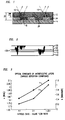
- FIG.1 is an illustration of how a typical lithographic exposure gives rise to unwanted reflections that expose portions of the energy sensitive resist material to radiation that are not desired to be so exposed.
- FIG. 2 is an illustration of the anti-reflection coating of the present invention.
- FIG. 3 illustrates the relationship between the flow rates of the reactant gases used to form the anti-reflection coating of the present invention and the real and imaginary indices of the coating.
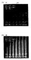
- FIG. 4A is a photograph of lines formed over a topographic substrate without the anti-reflective coating of the present invention.
- FIG. 4B is a photograph of features formed over a topographic substrate with the anti-reflective coating of the present invention formed thereover.
- the present invention is directed to an anti-reflective coating (ARC) for use in lithographic processes for device fabrication.
- the anti-reflective coating of the present invention has at least two different indices of refraction.
- the first index of refraction is at the top interface (previously defined as the interface between the ARC and the overlying layer of energy sensitive resist material).
- the second index of refraction is in a plane intermediate between the top interface and the bottom interface (previously defined as the interface between the ARC and the substrate underlying the ARC) or at the bottom interface.
- the energy transmitted into the ARC is absorbed by the ARC, so that no adverse lithographic consequences result from the reflection of radiation at the bottom interface of the ARC layer. Consequently, the ARC layer is made of a material that absorbs radiation at the wavelength of the exposing radiation. It is advantageous if the material is a silicon-containing oxide, wherein the amount of silicon is greater than the stoichiometric amount relative to the amount of oxide in the film.
- the ARC layer of the present invention prevents the reflection of any significant energy from the substrate surface, back into the energy sensitive resist material.
- "significant energy" means energy that is sufficient to cause adverse lithographic consequences.
- the ARC of the present invention is either a single layer with a first index of refraction and a second index of refraction as previously described, or a plurality of layers, each layer having a different index of refraction. It is advantageous if the index of refraction at the top interface is close to the index of refraction of the overlying photoresist layer. In the context of the present invention, it is advantageous if the refractive index is within about 10 percent of the index of refraction of the overlying photoresist.
- the refractive index referred to above is the real portion of the refractive index at the wavelength of the incident radiation.
- the ARC also has a different absorption at the top interface than at the bottom interface.
- refractive index refers to the real component of the refractive index.
- FIG. 2 illustrates the embodiment of the present invention wherein the ARC has multiple layers of non-stoichiometric silicon oxide.
- the ARC 100 has three layers, 110, 120 and 130.
- the ARC is formed over a substrate 140.
- the surface of the substrate is non-planar, i.e. topographic, because the ARC is used is to correct for problems associated with resist layers formed over topography.
- topography is not illustrated on the surface of the substrate depicted in FIG. 2.
- a layer of energy sensitive resist material 150 is formed over the ARC.
- the resist material is a conventional deep-ultraviolet (248 nm) resist, because these resist materials are easily index matched with silicon-containing oxide materials.
- the resist layer 150 is a conventional deep UV resist such as ARCH 2® which is obtained commercially from Olin Cieby Giegy.
- ARCH 2® is a registered trademark of Olin Cieby Giegy.
- an ARC with a top layer 130 that has a refractive index of about 1.82 + i0.23 is contemplated as suitable.
- Such a layer 130 is formed using conventional apparatus and conditions for forming a silicon-containing oxide film. The desired index is obtained by controlling the flow rate of the nitrous oxide relative to the silane to about 4:1.
- the ARC of the present invention is intended to absorb substantially all of the radiation incident thereon, it must absorb at the relevant wavelength and have a sufficient thickness to attenuate the incident radiation.
- the thickness of the top layer 130 is selected to be 25 nm.
- the thickness of the ARC layer or layers will vary depending upon the absorption of the ARC layer material at the wavelength of the incident radiation.
- the thickness of the ARC layer or layers while largely a matter of design choice, is selected based upon the amount of reflectivity which can be tolerated in the lithographic process and the contstraints imposed by process integration.
- the intermediate ARC layer 120 has a refractive index of 1.95 + i 0.45.
- the real component of the refractive index is sufficiently close to the refractive index of the layer 130 so that the amount of reflection at the interface of layers 120 and 130 is within lithographic tolerances.
- the absorption of layer 120 is greater than the absorption of layer 130, so that layer 120 absorbs more of the incident radiation through its thickness.
- the thickness of layer 120 is also selected to be 25 nm.
- Layer 120 is formed using a flow rate ratio of nitrous oxide to silane of about 2:1.
- the bottom ARC layer 110 has a refractive index of 2.1 + i 1.01.
- the real component of the refractive index is sufficiently close to the refractive index of the layer 120 so that the amount of reflection at the interface of layers 120 and 110 is within lithographic tolerances.
- the absorption of layer 110 is greater than the absorption of layer 120, so that layer 110 absorbs more of the incident radiation through its thickness.
- the thickness of layer 110 is selected to be 30 nm in order to obtain the desired degree of absorption.
- Layer 110 is formed using a flow rate ratio of nitrous oxide to silane of about 1.25:1.
- the index of refraction of the material is varied by varying the composition of the ARC.
- the composition is varied by varying the flow rates of the silane gas relative to the nitrous oxide gas. Since the composition of the film is a function of the flow rates of the nitrous oxide and silane into the chamber, it follows that the refractive index (both the real and imaginary components) is a function of the flow rate of these reactants. This is illustrated in FIG. 3, which is a graph of both the real and imaginary components of the refractive index as a function of the ratio of the flow rates of nitrous oxide and silane.
- FIG. 3 is a graph of both the real and imaginary components of the refractive index as a function of the ratio of the flow rates of nitrous oxide and silane.
- a film with a refractive index of about 1.82 + i0.23 is obtained when the nitrous oxide/silane flow rate ratio is about 4:1.
- a film with a refractive index of about 1.95 + i0.45 was obtained with a nitrous oxide/silane flow rate ratio of about 2:1.
- a film with a refractive index of about 2.1 + i1.01 was obtained with a nitrous oxide/silane flow rate ratio of about 1.25:1.
- a 200 nm thick layer of silicon dioxide was formed on a 5-inch silicon wafer using conventional expedients well known to one skilled in the art.
- a layer of photoresist was formed over the oxide layer and then patternwise exposed using a reticle with a grating that defines 800 nm lines and spaces.
- the pattern was developed using conventional expedients and the pattern was then transferred into the underlying oxide layer, thereby forming a pattern of 800 nm lines and spaces with a step height of 200 nm on the substrate surface.
- a 200 nm-thick layer of polysilicon was then formed on the patterned wafer, again using conventional expedients.
- a trilayer ARC was formed on the lot B wafers by placing each wafer individually in a chamber equipped with supply lines for silane gas and for nitrous oxide.
- a first layer of silicon-containing oxide was formed on the substrate by introducing the silane and nitrous oxide into the chamber of an Applied Materials Model 5000 plasma deposition apparatus at respective flow rates of 200 sccm and 250 sccm.
- the chamber pressure was 2.5 torr and the power was 125 Watts.
- the wafer temperature was about 410°C.
- the plasma susceptor was placed about 350 mils from the wafer. Under these conditions, a 350 ⁇ -thick layer was formed on the substrate in about 2 seconds.
- the composition of the layer was SiO 0.54 .
- the index of refraction of this layer was determined to be 2.127 (real component) + i1.015 (imaginary component). All of the refractive indices reported in this example were measured using ellipsometry at 256 nm.
- a second layer was then formed on the layer described above under the same conditions, except the flow rate of the nitrous oxide was increased to 600 sccm.
- the thickness of the resulting layer was about 250 ⁇ .
- the composition of the resulting layer, determined as described above, was SiO 0.79 .
- the deposition time was 1.8 seconds and the index of refraction of the resulting layer was 1.93 + i0.433.
- a third layer was then formed on the layer described above under the same conditions, except the flow rate of the nitrous oxide was increased to 800 sccm for 1.7 seconds.
- the resulting layer had a thickness of about 300 ⁇ and an index of refraction of 1.852 + i0.265.
- Wafers from lots A (no ARC layer) and B (ARC layer formed thereon) were then coated with a 70 nm thick layer of ARCH II® photoresist.
- the photoresist was then exposed to patterned 248 nm radiation using a deep UV stepper (GCA Model XLS) with a 0.53 numerical aperture.
- the radiation was patterned using a mask defining 250 nm lines and spaces and isolated features aligned perpendicular to the topography.
- the wafers were then baked at 130°C and the patterns were developed using a solution of tetra methyl ammonium hydroxide and deionized water.
- FIG. 4A is a photograph of the lines developed on a wafer in lot A.
- the lines 200 have a variable width.
- the lines have one width where they overly the raised portions of the underlying topography and another width where they do not overly the raised portions of the underlying topography. This indicates that a different amount of radiation was introduced into this portion of the resist than in the other portions of the exposed resist. No such width variations are observed in FIG. 4B, which is a photograph of the lines developed on a wafer in lot B.
Landscapes
- Engineering & Computer Science (AREA)
- Architecture (AREA)
- Structural Engineering (AREA)
- Physics & Mathematics (AREA)
- General Physics & Mathematics (AREA)
- Exposure Of Semiconductors, Excluding Electron Or Ion Beam Exposure (AREA)
- Application Of Or Painting With Fluid Materials (AREA)
- Preparing Plates And Mask In Photomechanical Process (AREA)
Applications Claiming Priority (2)
| Application Number | Priority Date | Filing Date | Title |
|---|---|---|---|
| US61159596A | 1996-03-07 | 1996-03-07 | |
| US611595 | 1996-03-07 |
Publications (2)
| Publication Number | Publication Date |
|---|---|
| EP0794460A2 true EP0794460A2 (fr) | 1997-09-10 |
| EP0794460A3 EP0794460A3 (fr) | 1997-09-24 |
Family
ID=24449655
Family Applications (1)
| Application Number | Title | Priority Date | Filing Date |
|---|---|---|---|
| EP97301211A Withdrawn EP0794460A3 (fr) | 1996-03-07 | 1997-02-25 | Procédé de fabrication de dispositif et couche antiréfléchissante à cet effet |
Country Status (3)
| Country | Link |
|---|---|
| EP (1) | EP0794460A3 (fr) |
| JP (1) | JPH09326360A (fr) |
| KR (1) | KR970067548A (fr) |
Cited By (3)
| Publication number | Priority date | Publication date | Assignee | Title |
|---|---|---|---|---|
| EP0877415A3 (fr) * | 1997-05-07 | 2004-06-16 | Applied Materials, Inc. | Système et méthode pour le dépôt d'un film multicouche |
| CN115172432A (zh) * | 2022-08-09 | 2022-10-11 | 京东方科技集团股份有限公司 | 显示面板及其制备方法、显示装置 |
| WO2024147143A1 (fr) * | 2023-01-08 | 2024-07-11 | B.G. Negev Technologies And Applications Ltd., At Ben-Gurion University | Structure antireflet durcissable aux uv de nano-impression et son procédé de création |
Families Citing this family (2)
| Publication number | Priority date | Publication date | Assignee | Title |
|---|---|---|---|---|
| US6500773B1 (en) * | 2000-11-27 | 2002-12-31 | Applied Materials, Inc. | Method of depositing organosilicate layers |
| CN102904546B (zh) * | 2012-08-30 | 2016-04-13 | 中兴通讯股份有限公司 | 一种温度补偿能力可调节的压电声波谐振器 |
Family Cites Families (2)
| Publication number | Priority date | Publication date | Assignee | Title |
|---|---|---|---|---|
| JPS6054433A (ja) * | 1983-09-05 | 1985-03-28 | Hitachi Ltd | パタ−ン形成法 |
| EP0379924A3 (fr) * | 1989-01-23 | 1990-11-07 | Siemens Aktiengesellschaft | Procédé pour réduire la variation de la grandeur des structures dans une couche de couverture par suite de la réflexion engendrée par la lithographie optique utilisée pour la fabrication d'un circuit intégré |
-
1997
- 1997-02-24 JP JP9038885A patent/JPH09326360A/ja active Pending
- 1997-02-25 EP EP97301211A patent/EP0794460A3/fr not_active Withdrawn
- 1997-03-06 KR KR1019970007444A patent/KR970067548A/ko not_active Withdrawn
Cited By (3)
| Publication number | Priority date | Publication date | Assignee | Title |
|---|---|---|---|---|
| EP0877415A3 (fr) * | 1997-05-07 | 2004-06-16 | Applied Materials, Inc. | Système et méthode pour le dépôt d'un film multicouche |
| CN115172432A (zh) * | 2022-08-09 | 2022-10-11 | 京东方科技集团股份有限公司 | 显示面板及其制备方法、显示装置 |
| WO2024147143A1 (fr) * | 2023-01-08 | 2024-07-11 | B.G. Negev Technologies And Applications Ltd., At Ben-Gurion University | Structure antireflet durcissable aux uv de nano-impression et son procédé de création |
Also Published As
| Publication number | Publication date |
|---|---|
| JPH09326360A (ja) | 1997-12-16 |
| EP0794460A3 (fr) | 1997-09-24 |
| KR970067548A (ko) | 1997-10-13 |
Similar Documents
| Publication | Publication Date | Title |
|---|---|---|
| US5968324A (en) | Method and apparatus for depositing antireflective coating | |
| US5234780A (en) | Exposure mask, method of manufacturing the same, and exposure method using the same | |
| US6514667B2 (en) | Tunable vapor deposited materials as antireflective coatings, hardmasks and as combined antireflective coating/hardmasks and methods of fabrication thereof and applications thereof | |
| US20080118866A1 (en) | Method for forming a tunable deep-ultrviolet dielectric antireflection layer for image transfer processing | |
| US5437961A (en) | Method of manufacturing semiconductor device | |
| US5580701A (en) | Process for elimination of standing wave effect of photoresist | |
| CN1971424A (zh) | 半导体结构及使用其形成光刻胶图形和半导体图形的方法 | |
| US6399481B1 (en) | Method for forming resist pattern | |
| Babich et al. | Hardmask technology for sub-100-nm lithographic imaging | |
| EP0794460A2 (fr) | Procédé de fabrication de dispositif et couche antiréfléchissante à cet effet | |
| Cirelli et al. | A multilayer inorganic antireflective system for use in 248 nm deep ultraviolet lithography | |
| US6200734B1 (en) | Method for fabricating semiconductor devices | |
| US5543252A (en) | Method for manufacturing exposure mask and the exposure mask | |
| JPH1131650A (ja) | 反射防止膜、被処理基板、被処理基板の製造方法、微細パターンの製造方法、および半導体装置の製造方法 | |
| JP3339156B2 (ja) | 微細パターンの製造方法と半導体装置の製造方法 | |
| JP2560773B2 (ja) | パターン形成方法 | |
| US6815367B2 (en) | Elimination of resist footing on tera hardmask | |
| KR100274149B1 (ko) | 금속막 패턴닝 방법 | |
| Xu et al. | Double-layer inorganic antireflective system for KrF lithography | |
| KR0174951B1 (ko) | 미세 패턴 형성 방법 | |
| JP3542334B2 (ja) | 半導体装置の製造方法 | |
| KR100966980B1 (ko) | 반도체 소자의 cd보상 방법 | |
| JPH0697065A (ja) | 微細レジストパターンの形成方法 | |
| Tanaka et al. | Precise pattern delineation by refractive index matching in a trilayer resist system | |
| JPH09180981A (ja) | 反射防止膜及びその形成方法、並びに半導体装置の製造方法 |
Legal Events
| Date | Code | Title | Description |
|---|---|---|---|
| PUAI | Public reference made under article 153(3) epc to a published international application that has entered the european phase |
Free format text: ORIGINAL CODE: 0009012 |
|
| PUAL | Search report despatched |
Free format text: ORIGINAL CODE: 0009013 |
|
| AK | Designated contracting states |
Kind code of ref document: A2 Designated state(s): DE FR GB |
|
| AK | Designated contracting states |
Kind code of ref document: A3 Designated state(s): DE FR GB |
|
| 17P | Request for examination filed |
Effective date: 19980312 |
|
| STAA | Information on the status of an ep patent application or granted ep patent |
Free format text: STATUS: THE APPLICATION IS DEEMED TO BE WITHDRAWN |
|
| 18D | Application deemed to be withdrawn |
Effective date: 20000830 |