EP0794525B1 - Appareil de conversion d'éléments d'image - Google Patents
Appareil de conversion d'éléments d'image Download PDFInfo
- Publication number
- EP0794525B1 EP0794525B1 EP97301375A EP97301375A EP0794525B1 EP 0794525 B1 EP0794525 B1 EP 0794525B1 EP 97301375 A EP97301375 A EP 97301375A EP 97301375 A EP97301375 A EP 97301375A EP 0794525 B1 EP0794525 B1 EP 0794525B1
- Authority
- EP
- European Patent Office
- Prior art keywords
- video signal
- signal
- conversion
- horizontal
- interpolation
- Prior art date
- Legal status (The legal status is an assumption and is not a legal conclusion. Google has not performed a legal analysis and makes no representation as to the accuracy of the status listed.)
- Expired - Lifetime
Links
Images



Classifications
-
- G—PHYSICS
- G09—EDUCATION; CRYPTOGRAPHY; DISPLAY; ADVERTISING; SEALS
- G09G—ARRANGEMENTS OR CIRCUITS FOR CONTROL OF INDICATING DEVICES USING STATIC MEANS TO PRESENT VARIABLE INFORMATION
- G09G3/00—Control arrangements or circuits, of interest only in connection with visual indicators other than cathode-ray tubes
- G09G3/20—Control arrangements or circuits, of interest only in connection with visual indicators other than cathode-ray tubes for presentation of an assembly of a number of characters, e.g. a page, by composing the assembly by combination of individual elements arranged in a matrix no fixed position being assigned to or needed to be assigned to the individual characters or partial characters
- G09G3/34—Control arrangements or circuits, of interest only in connection with visual indicators other than cathode-ray tubes for presentation of an assembly of a number of characters, e.g. a page, by composing the assembly by combination of individual elements arranged in a matrix no fixed position being assigned to or needed to be assigned to the individual characters or partial characters by control of light from an independent source
- G09G3/36—Control arrangements or circuits, of interest only in connection with visual indicators other than cathode-ray tubes for presentation of an assembly of a number of characters, e.g. a page, by composing the assembly by combination of individual elements arranged in a matrix no fixed position being assigned to or needed to be assigned to the individual characters or partial characters by control of light from an independent source using liquid crystals
-
- G—PHYSICS
- G09—EDUCATION; CRYPTOGRAPHY; DISPLAY; ADVERTISING; SEALS
- G09G—ARRANGEMENTS OR CIRCUITS FOR CONTROL OF INDICATING DEVICES USING STATIC MEANS TO PRESENT VARIABLE INFORMATION
- G09G5/00—Control arrangements or circuits for visual indicators common to cathode-ray tube indicators and other visual indicators
- G09G5/003—Details of a display terminal, the details relating to the control arrangement of the display terminal and to the interfaces thereto
- G09G5/005—Adapting incoming signals to the display format of the display terminal
-
- G—PHYSICS
- G09—EDUCATION; CRYPTOGRAPHY; DISPLAY; ADVERTISING; SEALS
- G09G—ARRANGEMENTS OR CIRCUITS FOR CONTROL OF INDICATING DEVICES USING STATIC MEANS TO PRESENT VARIABLE INFORMATION
- G09G3/00—Control arrangements or circuits, of interest only in connection with visual indicators other than cathode-ray tubes
- G09G3/20—Control arrangements or circuits, of interest only in connection with visual indicators other than cathode-ray tubes for presentation of an assembly of a number of characters, e.g. a page, by composing the assembly by combination of individual elements arranged in a matrix no fixed position being assigned to or needed to be assigned to the individual characters or partial characters
- G09G3/34—Control arrangements or circuits, of interest only in connection with visual indicators other than cathode-ray tubes for presentation of an assembly of a number of characters, e.g. a page, by composing the assembly by combination of individual elements arranged in a matrix no fixed position being assigned to or needed to be assigned to the individual characters or partial characters by control of light from an independent source
- G09G3/36—Control arrangements or circuits, of interest only in connection with visual indicators other than cathode-ray tubes for presentation of an assembly of a number of characters, e.g. a page, by composing the assembly by combination of individual elements arranged in a matrix no fixed position being assigned to or needed to be assigned to the individual characters or partial characters by control of light from an independent source using liquid crystals
- G09G3/3611—Control of matrices with row and column drivers
-
- H—ELECTRICITY
- H04—ELECTRIC COMMUNICATION TECHNIQUE
- H04N—PICTORIAL COMMUNICATION, e.g. TELEVISION
- H04N7/00—Television systems
- H04N7/01—Conversion of standards, e.g. involving analogue television standards or digital television standards processed at pixel level
- H04N7/0135—Conversion of standards, e.g. involving analogue television standards or digital television standards processed at pixel level involving interpolation processes
-
- G—PHYSICS
- G09—EDUCATION; CRYPTOGRAPHY; DISPLAY; ADVERTISING; SEALS
- G09G—ARRANGEMENTS OR CIRCUITS FOR CONTROL OF INDICATING DEVICES USING STATIC MEANS TO PRESENT VARIABLE INFORMATION
- G09G2340/00—Aspects of display data processing
- G09G2340/04—Changes in size, position or resolution of an image
- G09G2340/0407—Resolution change, inclusive of the use of different resolutions for different screen areas
- G09G2340/0414—Vertical resolution change
-
- G—PHYSICS
- G09—EDUCATION; CRYPTOGRAPHY; DISPLAY; ADVERTISING; SEALS
- G09G—ARRANGEMENTS OR CIRCUITS FOR CONTROL OF INDICATING DEVICES USING STATIC MEANS TO PRESENT VARIABLE INFORMATION
- G09G2340/00—Aspects of display data processing
- G09G2340/04—Changes in size, position or resolution of an image
- G09G2340/0407—Resolution change, inclusive of the use of different resolutions for different screen areas
- G09G2340/0421—Horizontal resolution change
-
- G—PHYSICS
- G09—EDUCATION; CRYPTOGRAPHY; DISPLAY; ADVERTISING; SEALS
- G09G—ARRANGEMENTS OR CIRCUITS FOR CONTROL OF INDICATING DEVICES USING STATIC MEANS TO PRESENT VARIABLE INFORMATION
- G09G2340/00—Aspects of display data processing
- G09G2340/04—Changes in size, position or resolution of an image
- G09G2340/0442—Handling or displaying different aspect ratios, or changing the aspect ratio
-
- G—PHYSICS
- G09—EDUCATION; CRYPTOGRAPHY; DISPLAY; ADVERTISING; SEALS
- G09G—ARRANGEMENTS OR CIRCUITS FOR CONTROL OF INDICATING DEVICES USING STATIC MEANS TO PRESENT VARIABLE INFORMATION
- G09G5/00—Control arrangements or circuits for visual indicators common to cathode-ray tube indicators and other visual indicators
- G09G5/003—Details of a display terminal, the details relating to the control arrangement of the display terminal and to the interfaces thereto
- G09G5/006—Details of the interface to the display terminal
-
- G—PHYSICS
- G09—EDUCATION; CRYPTOGRAPHY; DISPLAY; ADVERTISING; SEALS
- G09G—ARRANGEMENTS OR CIRCUITS FOR CONTROL OF INDICATING DEVICES USING STATIC MEANS TO PRESENT VARIABLE INFORMATION
- G09G5/00—Control arrangements or circuits for visual indicators common to cathode-ray tube indicators and other visual indicators
- G09G5/18—Timing circuits for raster scan displays
Definitions
- the present invention relates to a pixel conversion apparatus in an electronic equipment field taking a liquid crystal display as a representative. It relates to a pixel conversion apparatus, especially used when the number of pixels of the display area is different from the number of pixels of the input signal.
- a pixel conversion apparatus For displaying a picture on a display device such as a liquid crystal panel having different number of pixels from the pixels of an input signal, a pixel conversion apparatus is used.
- a pixel conversion apparatus in accordance with the prior art is explained below, referring to the drawing, to explain a function of scanning line conversion.
- FIG. 1 is a block diagram of a pixel conversion apparatus in accordance with the prior art in the case of a reduction conversion.
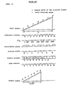
- FIG. 2 is a chart explaining a function of interpolating reduction conversion.
- the block 20 is a reference counter.
- the block 21 is a comparator.
- the block 22 is a register.
- the block 23 is an adder.
- the block 24 is an interpolation circuit.
- the block 25 is a memory.
- the block 26 is an address generator.
- FIG. 2 shows a functional principle at reduction factor is 0.6. In FIG. 2, short vertical lines of input signal express sample values of the original signal and the black dots express the values necessary to be newly made by interpolation.
- a reciprocal of the reduction factor SH (standard picture size) / (size to be reduced) is inputted from, for example a microcomputer.
- the signal SH is applied to a ⁇ SH circuit 27 composed of register 22 and adder 23.
- ⁇ SH circuit 27 integrates the input signal at the output of comparator 21 at every time an incidence pulse appears.
- the integer part of the output signal of ⁇ SH circuit 27 which is an integral output is compared with the output of reference counter 20 and comparator 21 outputs an incidence pulse when the values are equal.
- the incidence pulse indicates a position of a sample point to be interpolated, while the decimal part of the output signal of ⁇ SH circuit 27 is used as an interpolation coefficient at the moment.
- the sample value obtained as a result of interpolation is written in a designated position on the main memory according to a writing address made from the coincidence pulse at the counter.
- a reduced image can be formed on the memory by interpolating new pixel data at a generation of coincidence pulse and writing in a main memory, if it is read at a standard speed and is D/A converted, a reduced analog image signal is obtained.
- An example of a horizontal reduction is described but it is similar in a vertical reduction and in this case, a pulse synchronized with a horizontal sync signal takes a part of the clock signal.
- a signal of 832 horizontal dots and 640 horizontal effective dots is included in a standard decided at VESA (Video Electronics Standards Association).
- VESA Video Electronics Standards Association
- the number is an odd number with a decimal part and a normal display can not be obtained on this panel.
- the number of horizontal dots is larger than 1280 (standard of XGA), a part of image does not fill the specifications of a liquid crystal panel and it is sometimes impossible to display.
- a composition to display on a panel having VGA of 640x480 pixels by doubling the number of scanning lines is generally used.
- a composition to convert the number of scanning lines into double by writing the input signal into a FIFO (first in and first out) and reading a line twice at a double speed of the writing is generally used.
- the composition is simple and there is no need of a field memory and only an FIFO (line memory) is necessary but the vertical resolution deteriorates because it is not interlaced.
- a field memory such as movement adaptive type scanning line interpolation is necessary.
- a plurality of clock signal generation circuits for writing and reading into and from a memory used for a pixel conversion of the prior art is explained below and a plurality of PLL (phase locked loop) circuits having the same composition are merely used for generating each clock signal.
- PLL phase locked loop
- FIG. 3 is a block diagram of a video display apparatus in accordance with the prior art.
- the block 1 is a sync separator.
- the block 2 is a first phase detector.
- the block 3 is a first LPF (low pass filter).
- the block 4 is a first VCO (voltage controlled oscillator).
- the block 5 is a first counter.
- the block 6 is a first PLL composed of first phase detector 2, first LPF 3, first VCO 4 and first counter 5.
- the block 7 is a pixel converter.
- the block 8 is a second phase detector.
- the block 9 is a second LPF.
- the block 10 is a second VCO.
- the block 11 is a second counter.
- the block 12 is a second PLL composed of second phase detector 8, second LPF 9, second VCO 10 and second counter 11.
- the block 13 is a timing signal generator.
- a composite video signal inputted from an outside is supplied to pixel converter 7, an expansion or a reduction is processed by a clock signal from first PLL 6 and a clock signal from second PLL 12. (Clock signals having different frequencies are used between the input and the output.)
- the composite video signal inputted from the outside is also supplied to sync separator 1 at the same time.
- sync separator 1 only a sync signal is extracted from the composite video signal.
- a horizontal sync signal separated at sync separator 1 is supplied to first phase comparator 2.
- the PWM (pulse width modulation) output of first phase comparator 2 is supplied to first LPF 3.
- the response characteristic of first PLL 6 is almost decided at first LPF 3.
- Receiving an output of first LPF 3, first VCO 4 outputs a stable first clock signal.
- This first clock signal is used for driving a front stage of pixel converter 7. Further, the-first clock signal is frequency divided at an arbitrary rate at first counter 5 and is returned to first phase detector 2.
- a phase difference between two input signals is detected at first phase comparator 2.
- the output of first counter 5 is also supplied to second phase comparator 8.
- the response characteristic of second PLL 12 is decided at second LPF 9.
- the numbers of clocks per one horizontal period including a blanking period are not always the same, even if the number of effective display pixels of the two computers are the same.
- the operator of the computer or the software of the computer outputs a signal is quite arbitrary. Therefore, the oscillation frequency range of PLL circuit 42 must be wide and a lot of values must be previously stored for the number of clocks per one horizontal period.
- Qi D(i) x a + D(i+1) x b + D(i+2) x c + D(i+3) x d
- Qi is the i-th data after pixel conversion.
- D(i+1), D(i+2) and D(I+3) are the D(I+1)-th, the D(I+2)-th and the D(I+3)-th data before conversion, respectively.
- the values a, b, c and d of the input signal are decided by a ratio of number of pixels between before and after conversion and is obtained by calculating a contribution factor of the data before conversion against the data after conversion.
- the present invention provides a pixel conversion apparatus as defined in claim 1.
- a pixel conversion apparatus having the features of the preamble of claim 1 is disclosed in EP-A-0479 508.
- the timing generation means discriminates the number of pixels and the effective display area of the input signal. Further, the blanking period of the picture displaying the input signal is calculated from the discrimination result and the picture display area with the horizontal sync signal in the blanking period being made different from the effective picture area.
- the pixel conversion information analysis means discriminates which the input video signal is interlaced or non-interlaced, discriminates which the interlaced signal is in an odd field or in an even field and the interpolation means processes a different interpolation between for an odd field and for an even field according to the discrimination result of odd/even field.
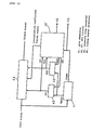
- FIGs. 6-8 An exemplary embodiment of the present invention is explained below referring to FIGs. 6-8.
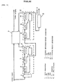
- FIG. 6 is a pixel conversion apparatus in accordance with an exemplary embodiment of the present invention.
- the block 61 is a sync separator.
- the block 62 is a first PLL circuit for generating a first clock signal synchronizing with a horizontal sync signal of the input signal.
- the block 63 is a second PLL circuit for generating a second clock signal synchronizing with a horizontal sync signal of the input signal.
- the block 64 is a scanning line converter for converting the number of scanning lines of the input signal.
- the block 65 is a timing signal generator for generating an interpolation coefficient and an interpolation timing signal to interpolate the sample at scanning line converter 64 and generating a sync signal to drive a display device such as a liquid crystal panel.
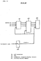
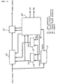
- FIG. 7 is an example of a block diagram of a timing signal generator.
- the block 76 is a first counter for generating a signal HD1 by dividing a first clock signal CK1 at an arbitrary rate.
- the block 77 is a horizontal interpolation circuit for generating an interpolation coefficient and a timing signal used at horizontal interpolation by using first clock signal CK1.
- the block 78 is a second counter for generating a signal HD2 by dividing second clock signal CK2 at an arbitrary rate.
- the block 79 is a vertical interpolation circuit for generating an interpolation coefficient and a timing signal used at vertical interpolation by using second clock signal CK2.
- the block 710 is a first H counter for generating a first horizontal sync signal a by counting second clock signal CK2.
- the block 711 is a second H counter for generating a second horizontal sync signal b by counting second clock signal CK2.
- the block 712 is a selector for selecting the output signal a of first H counter 710 or the output signal b of second H counter 711.
- the block 713 is a V counter for controlling selector 712 by counting a horizontal sync signal c which is an output of selector 712.
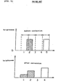
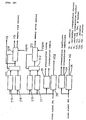
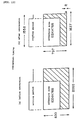
- FIG. 8 shows relations between the number of samples (horizontal) and the number of scanning lines (vertical) for three kinds of video signals.
- first PLL circuit 62 reproduces a first clock signal CK1 from Hsync.
- the frequency of first clock signal CK1 is decided at first PLL circuit 62 by setting a dividing ratio at first counter 76 in timing generator 65.
- a dot clock signal at the signal sending side can be reproduced by setting the dividing ratio 800.
- a clock signal CK2 set at second counter 78 is similarly generated at second PLL circuit 63.
- the dividing ratio of second counter 78 is set to 1280 similarly to XGA standard.
- Horizontal interpolation circuit 77 and vertical interpolation circuit 79 generate an interpolation coefficient and a timing signal converting from a VGA standard to an XGA standard and scanning line converter 64 converts the number of scanning lines.
- the input signal is converted from the relation between the number of samples and the number of scanning lines of CK1 shown in FIG. 8(a) to the relation between the number of samples and the number of scanning lines of CK2 shown in FIG. 8(b). That is, because the number of horizontal dots is converted from 800 dots to 1280 dots (1.6 times), the number of scanning lines in a vertical direction is also converted from 525 lines to 840 lines, that is 1.6 times.
- the number of scanning lines of a standard XGA signal is 806 lines, there is no room in the timing specifications for a picture display device such as a liquid crystal panel and some parts are not displayed for a signal with 840 lines.
- the output signal a of first H counter 710 and the output signal b of second H counter 711 are set 1280 and 2304, respectively and the number of lines is counted at V counter 713 and the output signal a or b is selected at the border of 768 lines.
- the image can be displayed on the liquid crystal panel.
- a timing of the horizontal sync signal is selected by using more than two H counters and a proper display can be obtained.
- composition it is possible to display a picture even on a display device having less room of timing without frame frequency conversion by providing with a plurality of horizontal sync signals during a frame period.
- the number of lines is not converted according to the ratio of the number of horizontal effective dots before conversion to the number of horizontal effective dots after conversion by selecting a horizontal sync signal having a plurality of horizontal frequencies in the same frame, the conversion ratio of a horizontal direction can be made different from that of a vertical direction. As a result, the number of, scanning lines can be converted without any lack of picture on the display area.
- FIG. 9 is a memory.
- FIG. 10 is a block diagram of a timing signal generator 66 shown in FIG. 9.
- the block 715 is a third H counter.
- the block 716 is a fourth H counter.
- the block 717 is a second selector.
- the block 718 is a second V counter.
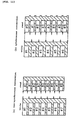
- FIGs. 11 and 12 are charts expressing frame frequency conversion.
- the comparative example although it is general to convert a frame frequency using a memory in the case in which timing specifications of a display device is not satisfied, in this case, if the memory writing and the memory reading are made with non-synchronized clocks as shown in FIG. 11(a), a jumping over of a frame before conversion occurs on the picture. That is, when the reading clock frequency is a little higher than the writing clock frequency, the read address passes over the write address while writing like #1 (the first) frame as shown in FIG. 11(a). Although the first frame is read at reading, on the way it changes to call out a frame signal one frame ahead. It has no problem in a still picture but in a moving picture, the frame jumps over on the effective picture area and it appears as an interference.
- the number of maximum horizontal dots is 1700 and the number of maximum scanning lines is 832 as timing specifications of a liquid crystal panel
- the number of total clocks before conversion m is decided by H counter 710 or 711 and V counter 713 and the number of total clocks after conversion n is decided by H counter 715 or 716 and V counter 718.
- a scanning line conversion is done without frame jumping over or discontinuous displaying.
Landscapes
- Engineering & Computer Science (AREA)
- Theoretical Computer Science (AREA)
- Physics & Mathematics (AREA)
- Computer Hardware Design (AREA)
- General Physics & Mathematics (AREA)
- Crystallography & Structural Chemistry (AREA)
- Chemical & Material Sciences (AREA)
- Multimedia (AREA)
- Signal Processing (AREA)
- Liquid Crystal Display Device Control (AREA)
- Control Of Indicators Other Than Cathode Ray Tubes (AREA)
- Television Systems (AREA)
- Transforming Electric Information Into Light Information (AREA)
- Controls And Circuits For Display Device (AREA)
Claims (2)
- Dispositif de conversion de pixels pour convertir un signal vidéo d'entrée possédant un premier format en un signal vidéo de sortie possédant un second format, qui est différent dudit premier format, le signal vidéo d'entrée et le signal vidéo de sortie possédant des trames ayant deux parties du signal vidéo, comprenant chacune une série de lignes de balayage successives, qui sont délimitées par des signaux de synchronisation horizontale et verticale (Hsync, Vsync), dans lequel la première partie du signal est une partie de signal vidéo effective qui contient l'information d'image, et la seconde partie du signal est une partie de signal vidéo de suppression, qui ne contient aucune information d'image et qui succède dans le temps à la partie effective du signal vidéo, ledit dispositif comprenant :caractérisé en ce que les moyens de production de cadencement (710,711,712,713) sont en outre agencés de manière à délivrer le premier signal de synchronisation horizontale conformément à un premier nombre d'impulsions d'horloge pour chaque ligne de balayage dans la partie effective du signal vidéo et délivrer un second signal de synchronisation horizontale conformément à un second nombre des impulsions d'horloge pour chaque ligne de balayage dans la partie du signal vidéo de suppression; ledit second nombre d'impulsions d'horloge étant différent dudit premier nombre d'impulsions d'horloge, de telle sorte que (i) le nombre de lignes de balayage successives dans la partie effective du signal vidéo après la conversion est égal au nombre de lignes requises pour la partie effective dudit signal vidéo de sortie et de telle sorte que (ii) le nombre total de lignes de balayage successives dans la partie effective du signal vidéo et dans la partie de suppression du signal vidéo après la conversion est sensiblement égal au nombre total de lignes requises pour la partie effective du signal vidéo et la partie de suppression du signal vidéo dans ledit second format.des moyens de séparation de synchronisation (61) pour séparer les signaux de synchronisation horizontale et verticale (Hsync, Vsync) dudit signal vidéo d'entrée;des moyens (62,63,64,76,78) de conversion de pixels pour déterminer comment convertir des signaux de pixels dudit signal vidéo d'entrée en des pixels du signal vidéo de sortie pour délivrer des impulsions d'horloge pour le signal vidéo de sortie, chaque impulsion d'horloge étant associée à un pixel, et pour exécuter ladite conversion de telle sorte que le format des images du signal vidéo de sortie est égal au format de l'image du signal vidéo d'entrée;des moyens d'interpolation (77,79) pour interpoler au moins une partie desdits pixels délivrés par lesdits moyens de conversion de pixels (62,63,64,76,78); etdes moyens de production de cadencement (710, 711,712,713), qui sont agencés de manière à délivrer un premier signal de synchronisation horizontale pour chaque ligne de balayage de la partie effective du signal vidéo conformément au second format sur la base des signaux de sortie des moyens de conversion de pixels (62,63,64,76,78);
- Dispositif de conversion de pixels selon la revendication 1, dans lequel les moyens de conversion de pixels (62,63,64,76,78) comprennent :un premier circuit PLL (62) pour produire un premier signal d'horloge (CK1) réalisant une synchronisation avec les signaux séparés de synchronisation horizontale (HSYNC) délivrés par lesdits moyens de séparation de synchronisation;un second circuit PLL (63) pour produire un second signal d'horloge (CK2) synchronisant le second signal d'horloge (CK2) constituant les impulsions d'horloge avec lesdits signaux séparés de synchronisation horizontale (HSYNC);un circuit (64) de conversion de lignes de balayage pour (i) convertir le nombre de lignes de balayage dudit signal vidéo d'entrée en un autre nombre de lignes de balayage, et pour convertir le nombre de pixels par ligne de balayage en un autre nombre de pixels pour chaque ligne de balayage et pour (ii) délivrer ledit signal vidéo de sortie; etdans lequel les moyens de production de cadencement (710,711,712,713) comprennent en outre lesdits moyens d'interposition (77,79), qui sont agencés de manière à i) produire un signal de cadencement d'interpolation et un coefficient d'interpolation pour une interpolation horizontale dans ledit circuit (44) de conversion de lignes de balayage en réponse au premier signal d'horloge (CK1), et ii) produire un signal de cadencement d'interpolation et un coefficient d'interpolation pour une interpolation musicale dans ledit circuit (64) de conversion de lignes de balayage en réponse au second signal d'horloge (CK2).
Applications Claiming Priority (12)
| Application Number | Priority Date | Filing Date | Title |
|---|---|---|---|
| JP4860596 | 1996-03-06 | ||
| JP48605/96 | 1996-03-06 | ||
| JP8048604A JPH09244586A (ja) | 1996-03-06 | 1996-03-06 | 映像表示装置 |
| JP48604/96 | 1996-03-06 | ||
| JP4860496 | 1996-03-06 | ||
| JP04860596A JP3259627B2 (ja) | 1996-03-06 | 1996-03-06 | 走査線変換装置 |
| JP4993696 | 1996-03-07 | ||
| JP49936/96 | 1996-03-07 | ||
| JP04993696A JP3259628B2 (ja) | 1996-03-07 | 1996-03-07 | 走査線変換装置 |
| JP4993796 | 1996-03-07 | ||
| JP04993796A JP3803414B2 (ja) | 1996-03-07 | 1996-03-07 | 水平画素数変換回路 |
| JP49937/96 | 1996-03-07 |
Publications (3)
| Publication Number | Publication Date |
|---|---|
| EP0794525A2 EP0794525A2 (fr) | 1997-09-10 |
| EP0794525A3 EP0794525A3 (fr) | 1998-03-11 |
| EP0794525B1 true EP0794525B1 (fr) | 2003-07-23 |
Family
ID=27462234
Family Applications (1)
| Application Number | Title | Priority Date | Filing Date |
|---|---|---|---|
| EP97301375A Expired - Lifetime EP0794525B1 (fr) | 1996-03-06 | 1997-03-03 | Appareil de conversion d'éléments d'image |
Country Status (6)
| Country | Link |
|---|---|
| US (1) | US5933196A (fr) |
| EP (1) | EP0794525B1 (fr) |
| KR (1) | KR100246088B1 (fr) |
| CN (1) | CN1112027C (fr) |
| DE (1) | DE69723601T2 (fr) |
| TW (1) | TW322675B (fr) |
Families Citing this family (27)
| Publication number | Priority date | Publication date | Assignee | Title |
|---|---|---|---|---|
| US6380979B1 (en) | 1996-07-02 | 2002-04-30 | Matsushita Electric Industrial Co., Ltd. | Scanning line converting circuit and interpolation coefficient generating circuit |
| KR100225072B1 (ko) * | 1996-12-18 | 1999-10-15 | 윤종용 | 포멧 콘버터 |
| MY119346A (en) * | 1996-12-24 | 2005-05-31 | Sony Corp | Picture processing apparatus and method |
| JPH10198309A (ja) | 1996-12-27 | 1998-07-31 | Matsushita Electric Ind Co Ltd | 水平振幅調整回路と垂直振幅調整回路とその両調整回路を備えた液晶表示装置 |
| JPH10198302A (ja) | 1997-01-10 | 1998-07-31 | Matsushita Electric Ind Co Ltd | マルチスキャン型ディスプレイ装置 |
| US5739867A (en) * | 1997-02-24 | 1998-04-14 | Paradise Electronics, Inc. | Method and apparatus for upscaling an image in both horizontal and vertical directions |
| JP2000023063A (ja) | 1998-06-26 | 2000-01-21 | Sony Corp | 映像再生装置及び再生方法 |
| JP2000059735A (ja) * | 1998-08-04 | 2000-02-25 | Sony Corp | 画像処理装置および方法、並びに提供媒体 |
| EP1001353A1 (fr) * | 1998-11-10 | 2000-05-17 | Sony Corporation | Dispositif et procédés d'interpolation et dispositf d'affichage d'image |
| KR100281885B1 (ko) * | 1998-12-28 | 2001-02-15 | 윤종용 | 디지털 신호 수신장치의 클럭 주파수 변환장치 |
| JP2000305555A (ja) * | 1999-04-19 | 2000-11-02 | Sony Corp | 画像表示装置 |
| JP4686800B2 (ja) * | 1999-09-28 | 2011-05-25 | 三菱電機株式会社 | 画像表示装置 |
| JP3998399B2 (ja) * | 1999-12-03 | 2007-10-24 | 松下電器産業株式会社 | 映像信号変換装置 |
| JP2001175231A (ja) * | 1999-12-17 | 2001-06-29 | Sony Corp | 同期周波数の変換回路 |
| JP2001320680A (ja) * | 2000-05-09 | 2001-11-16 | Sony Corp | 信号処理装置および方法 |
| JP4691812B2 (ja) * | 2001-03-29 | 2011-06-01 | ソニー株式会社 | 係数データの生成装置および生成方法、それを使用した情報信号の処理装置および処理方法 |
| US7071996B2 (en) * | 2002-07-19 | 2006-07-04 | Sun Microsystems, Inc. | Synchronizing video formats with dissimilar timing |
| KR100510550B1 (ko) * | 2003-09-29 | 2005-08-26 | 삼성전자주식회사 | 수평 및 수직 방향으로 영상을 스케일링하는 방법 및 장치 |
| US8542258B2 (en) * | 2004-05-05 | 2013-09-24 | Mstar Semiconductor, Inc. | Apparatus and method for increasing pixel resolution of image using coherent sampling |
| US7239355B2 (en) * | 2004-05-17 | 2007-07-03 | Mstar Semiconductor, Inc. | Method of frame synchronization when scaling video and video scaling apparatus thereof |
| TWI250801B (en) * | 2004-11-17 | 2006-03-01 | Realtek Semiconductor Corp | Method for generating a video clock and an associated target image frame |
| KR20060104811A (ko) * | 2005-03-31 | 2006-10-09 | 엘지전자 주식회사 | 영상표시기기의 화질 조정장치 및 방법 |
| TWI271104B (en) * | 2005-09-19 | 2007-01-11 | Novatek Microelectronics Corp | Device and method for zooming images |
| TWI463865B (zh) * | 2007-11-23 | 2014-12-01 | Mstar Semiconductor Inc | 多切割之水平同步訊號之產生裝置及方法 |
| CN101742081B (zh) * | 2009-12-11 | 2012-11-21 | 华亚微电子(上海)有限公司 | 图像稳定器 |
| JP6703800B2 (ja) * | 2016-04-01 | 2020-06-03 | シャープ株式会社 | 表示装置、表示装置の制御方法、および制御プログラム |
| US10699677B2 (en) * | 2016-09-27 | 2020-06-30 | Intel Corporation | Display controller to prevent visual artifacts with spread spectrum clocking |
Family Cites Families (12)
| Publication number | Priority date | Publication date | Assignee | Title |
|---|---|---|---|---|
| JP2526558B2 (ja) * | 1986-10-21 | 1996-08-21 | ソニー株式会社 | ビデオ信号のスキャンコンバ−タ装置 |
| US4872054A (en) * | 1988-06-30 | 1989-10-03 | Adaptive Video, Inc. | Video interface for capturing an incoming video signal and reformatting the video signal |
| JP2913797B2 (ja) * | 1990-08-10 | 1999-06-28 | ソニー株式会社 | 画像拡縮処理方法 |
| JP2673386B2 (ja) * | 1990-09-29 | 1997-11-05 | シャープ株式会社 | 映像表示装置 |
| US5095280A (en) * | 1990-11-26 | 1992-03-10 | Integrated Circuit Systems, Inc. | Dual dot clock signal generator |
| JP2618156B2 (ja) * | 1992-06-08 | 1997-06-11 | インターナショナル・ビジネス・マシーンズ・コーポレイション | ドット・マトリックス表示パネルの駆動方法、ドット・マトリックス表示パネル用駆動回路、ドット・マトリックス表示装置、及び、ドット・マトリックス表示装置を備えた情報処理システム |
| JP3032382B2 (ja) * | 1992-07-13 | 2000-04-17 | シャープ株式会社 | デジタル信号のサンプリング周波数変換装置 |
| US5331346A (en) * | 1992-10-07 | 1994-07-19 | Panasonic Technologies, Inc. | Approximating sample rate conversion system |
| US5473382A (en) * | 1992-11-04 | 1995-12-05 | Hitachi, Ltd. | Video signal converting apparatus for converting an interlace video signal into a non-interlace video signal for reduction |
| US5335074A (en) * | 1993-02-08 | 1994-08-02 | Panasonic Technologies, Inc. | Phase locked loop synchronizer for a resampling system having incompatible input and output sample rates |
| JPH07199891A (ja) * | 1993-12-28 | 1995-08-04 | Canon Inc | 表示制御装置 |
| DE4423214C2 (de) * | 1994-07-01 | 1998-02-12 | Harris Corp | Multinorm-Dekoder für Videosignale und Verfahren zum Dekodieren von Videosignalen |
-
1997
- 1997-03-03 EP EP97301375A patent/EP0794525B1/fr not_active Expired - Lifetime
- 1997-03-03 DE DE69723601T patent/DE69723601T2/de not_active Expired - Fee Related
- 1997-03-04 US US08/811,504 patent/US5933196A/en not_active Expired - Lifetime
- 1997-03-05 TW TW086102672A patent/TW322675B/zh active
- 1997-03-06 CN CN97103303A patent/CN1112027C/zh not_active Expired - Fee Related
- 1997-03-06 KR KR1019970007404A patent/KR100246088B1/ko not_active Expired - Fee Related
Also Published As
| Publication number | Publication date |
|---|---|
| EP0794525A3 (fr) | 1998-03-11 |
| CN1112027C (zh) | 2003-06-18 |
| KR100246088B1 (ko) | 2000-03-15 |
| US5933196A (en) | 1999-08-03 |
| KR970067077A (ko) | 1997-10-13 |
| EP0794525A2 (fr) | 1997-09-10 |
| CN1167397A (zh) | 1997-12-10 |
| DE69723601D1 (de) | 2003-08-28 |
| DE69723601T2 (de) | 2004-02-19 |
| TW322675B (fr) | 1997-12-11 |
Similar Documents
| Publication | Publication Date | Title |
|---|---|---|
| US5933196A (en) | Pixel conversion apparatus | |
| US5473381A (en) | Apparatus for converting frame format of a television signal to a display format for a high definition television (HDTV) receiver | |
| EP0479508B1 (fr) | Appareil d'affichage vidéo comportant un dispositif de visualisation possédant un agencement fixe bidimensionelle d'éléments d'image | |
| WO1998020670A2 (fr) | Procede et dispositif de conversion de signaux infographiques en signaux video tv avec changement d'echelles verticale et horizontale sans utilisation de tampon de trame | |
| US5029004A (en) | Edge enhancement apparatus useful with liquid crystal displays | |
| EP0821340B1 (fr) | Appareil de traitement de signal vidéo pour la conversion du signal pour l'adapter à un dispositif d'affichage | |
| EP0170869B2 (fr) | Procédé de conversion de balayage et unité de conversion de balayage utilisant ce procédé | |
| JPS6231289A (ja) | テレビジヨン表示方式 | |
| KR20000023800A (ko) | 주사 변환 장치 및 주사 변환 방법 | |
| US6219105B1 (en) | Video signal processing apparatus | |
| EP0746154B1 (fr) | Circuit de compression verticale d'un signal d'image incrustée | |
| US5404177A (en) | Double-picture type television receiver | |
| EP0515155B1 (fr) | Conversion du rythme de balayage | |
| JP3154190B2 (ja) | 汎用走査周期変換装置 | |
| JP3259627B2 (ja) | 走査線変換装置 | |
| US5552834A (en) | Apparatus for displaying an image in a reduced scale by sampling out an interlace video signal uniformly in a vertical direction without sampling out successive lines | |
| JP3259628B2 (ja) | 走査線変換装置 | |
| JP3909965B2 (ja) | 映像信号周波数変換装置 | |
| JP3128034B2 (ja) | 画像合成装置 | |
| EP1111917B1 (fr) | Procédé de calcul dynamique des phases d'interpolation dans un convertisseur de standards vidéo | |
| KR0164255B1 (ko) | 비디오 촬영용 영상신호 변환장치 | |
| KR100196845B1 (ko) | 컴퓨터와텔레비젼의영상신호인터페이스장치 | |
| KR0162346B1 (ko) | 광폭 티브이의 2화면 표시장치 | |
| JPH07134575A (ja) | 映像信号変換装置 | |
| JP3138148B2 (ja) | 映像信号変換装置 |
Legal Events
| Date | Code | Title | Description |
|---|---|---|---|
| PUAI | Public reference made under article 153(3) epc to a published international application that has entered the european phase |
Free format text: ORIGINAL CODE: 0009012 |
|
| AK | Designated contracting states |
Kind code of ref document: A2 Designated state(s): DE FR GB |
|
| PUAL | Search report despatched |
Free format text: ORIGINAL CODE: 0009013 |
|
| AK | Designated contracting states |
Kind code of ref document: A3 Designated state(s): DE FR GB |
|
| 17P | Request for examination filed |
Effective date: 19980518 |
|
| 17Q | First examination report despatched |
Effective date: 20000509 |
|
| GRAH | Despatch of communication of intention to grant a patent |
Free format text: ORIGINAL CODE: EPIDOS IGRA |
|
| GRAH | Despatch of communication of intention to grant a patent |
Free format text: ORIGINAL CODE: EPIDOS IGRA |
|
| GRAA | (expected) grant |
Free format text: ORIGINAL CODE: 0009210 |
|
| AK | Designated contracting states |
Designated state(s): DE FR GB |
|
| REG | Reference to a national code |
Ref country code: GB Ref legal event code: FG4D |
|
| REF | Corresponds to: |
Ref document number: 69723601 Country of ref document: DE Date of ref document: 20030828 Kind code of ref document: P |
|
| ET | Fr: translation filed | ||
| PLBE | No opposition filed within time limit |
Free format text: ORIGINAL CODE: 0009261 |
|
| STAA | Information on the status of an ep patent application or granted ep patent |
Free format text: STATUS: NO OPPOSITION FILED WITHIN TIME LIMIT |
|
| 26N | No opposition filed |
Effective date: 20040426 |
|
| PGFP | Annual fee paid to national office [announced via postgrant information from national office to epo] |
Ref country code: GB Payment date: 20090225 Year of fee payment: 13 |
|
| PGFP | Annual fee paid to national office [announced via postgrant information from national office to epo] |
Ref country code: DE Payment date: 20090226 Year of fee payment: 13 |
|
| PGFP | Annual fee paid to national office [announced via postgrant information from national office to epo] |
Ref country code: FR Payment date: 20090316 Year of fee payment: 13 |
|
| GBPC | Gb: european patent ceased through non-payment of renewal fee |
Effective date: 20100303 |
|
| REG | Reference to a national code |
Ref country code: FR Ref legal event code: ST Effective date: 20101130 |
|
| PG25 | Lapsed in a contracting state [announced via postgrant information from national office to epo] |
Ref country code: FR Free format text: LAPSE BECAUSE OF NON-PAYMENT OF DUE FEES Effective date: 20100331 |
|
| PG25 | Lapsed in a contracting state [announced via postgrant information from national office to epo] |
Ref country code: DE Free format text: LAPSE BECAUSE OF NON-PAYMENT OF DUE FEES Effective date: 20101001 |
|
| PG25 | Lapsed in a contracting state [announced via postgrant information from national office to epo] |
Ref country code: GB Free format text: LAPSE BECAUSE OF NON-PAYMENT OF DUE FEES Effective date: 20100303 |