EP0794567A2 - Verfahren zur Herstellung eines Speicherknotens mit Tiefgrabenstruktur für DRAM - Google Patents
Verfahren zur Herstellung eines Speicherknotens mit Tiefgrabenstruktur für DRAM Download PDFInfo
- Publication number
- EP0794567A2 EP0794567A2 EP97102901A EP97102901A EP0794567A2 EP 0794567 A2 EP0794567 A2 EP 0794567A2 EP 97102901 A EP97102901 A EP 97102901A EP 97102901 A EP97102901 A EP 97102901A EP 0794567 A2 EP0794567 A2 EP 0794567A2
- Authority
- EP
- European Patent Office
- Prior art keywords
- sidewall
- layer
- trench
- oxide
- resist
- Prior art date
- Legal status (The legal status is an assumption and is not a legal conclusion. Google has not performed a legal analysis and makes no representation as to the accuracy of the status listed.)
- Withdrawn
Links
Images

Classifications
-
- H—ELECTRICITY
- H10—SEMICONDUCTOR DEVICES; ELECTRIC SOLID-STATE DEVICES NOT OTHERWISE PROVIDED FOR
- H10B—ELECTRONIC MEMORY DEVICES
- H10B12/00—Dynamic random access memory [DRAM] devices
- H10B12/01—Manufacture or treatment
- H10B12/02—Manufacture or treatment for one transistor one-capacitor [1T-1C] memory cells
- H10B12/03—Making the capacitor or connections thereto
- H10B12/038—Making the capacitor or connections thereto the capacitor being in a trench in the substrate
-
- H—ELECTRICITY
- H10—SEMICONDUCTOR DEVICES; ELECTRIC SOLID-STATE DEVICES NOT OTHERWISE PROVIDED FOR
- H10B—ELECTRONIC MEMORY DEVICES
- H10B12/00—Dynamic random access memory [DRAM] devices
- H10B12/01—Manufacture or treatment
- H10B12/02—Manufacture or treatment for one transistor one-capacitor [1T-1C] memory cells
- H10B12/03—Making the capacitor or connections thereto
- H10B12/038—Making the capacitor or connections thereto the capacitor being in a trench in the substrate
- H10B12/0387—Making the trench
-
- H—ELECTRICITY
- H10—SEMICONDUCTOR DEVICES; ELECTRIC SOLID-STATE DEVICES NOT OTHERWISE PROVIDED FOR
- H10B—ELECTRONIC MEMORY DEVICES
- H10B12/00—Dynamic random access memory [DRAM] devices
- H10B12/30—DRAM devices comprising one-transistor - one-capacitor [1T-1C] memory cells
- H10B12/37—DRAM devices comprising one-transistor - one-capacitor [1T-1C] memory cells the capacitor being at least partially in a trench in the substrate
- H10B12/373—DRAM devices comprising one-transistor - one-capacitor [1T-1C] memory cells the capacitor being at least partially in a trench in the substrate the capacitor extending under or around the transistor
-
- H—ELECTRICITY
- H10—SEMICONDUCTOR DEVICES; ELECTRIC SOLID-STATE DEVICES NOT OTHERWISE PROVIDED FOR
- H10D—INORGANIC ELECTRIC SEMICONDUCTOR DEVICES
- H10D1/00—Resistors, capacitors or inductors
- H10D1/01—Manufacture or treatment
- H10D1/045—Manufacture or treatment of capacitors having potential barriers, e.g. varactors
- H10D1/047—Manufacture or treatment of capacitors having potential barriers, e.g. varactors of conductor-insulator-semiconductor capacitors, e.g. trench capacitors
-
- H—ELECTRICITY
- H10—SEMICONDUCTOR DEVICES; ELECTRIC SOLID-STATE DEVICES NOT OTHERWISE PROVIDED FOR
- H10D—INORGANIC ELECTRIC SEMICONDUCTOR DEVICES
- H10D1/00—Resistors, capacitors or inductors
- H10D1/60—Capacitors
- H10D1/68—Capacitors having no potential barriers
- H10D1/692—Electrodes
- H10D1/711—Electrodes having non-planar surfaces, e.g. formed by texturisation
-
- H—ELECTRICITY
- H10—SEMICONDUCTOR DEVICES; ELECTRIC SOLID-STATE DEVICES NOT OTHERWISE PROVIDED FOR
- H10W—GENERIC PACKAGES, INTERCONNECTIONS, CONNECTORS OR OTHER CONSTRUCTIONAL DETAILS OF DEVICES COVERED BY CLASS H10
- H10W10/00—Isolation regions in semiconductor bodies between components of integrated devices
- H10W10/01—Manufacture or treatment
- H10W10/011—Manufacture or treatment of isolation regions comprising dielectric materials
- H10W10/014—Manufacture or treatment of isolation regions comprising dielectric materials using trench refilling with dielectric materials, e.g. shallow trench isolations
- H10W10/0145—Manufacture or treatment of isolation regions comprising dielectric materials using trench refilling with dielectric materials, e.g. shallow trench isolations of trenches having shapes other than rectangular or V-shape
-
- H—ELECTRICITY
- H10—SEMICONDUCTOR DEVICES; ELECTRIC SOLID-STATE DEVICES NOT OTHERWISE PROVIDED FOR
- H10W—GENERIC PACKAGES, INTERCONNECTIONS, CONNECTORS OR OTHER CONSTRUCTIONAL DETAILS OF DEVICES COVERED BY CLASS H10
- H10W10/00—Isolation regions in semiconductor bodies between components of integrated devices
- H10W10/10—Isolation regions comprising dielectric materials
- H10W10/17—Isolation regions comprising dielectric materials formed using trench refilling with dielectric materials, e.g. shallow trench isolations
-
- Y—GENERAL TAGGING OF NEW TECHNOLOGICAL DEVELOPMENTS; GENERAL TAGGING OF CROSS-SECTIONAL TECHNOLOGIES SPANNING OVER SEVERAL SECTIONS OF THE IPC; TECHNICAL SUBJECTS COVERED BY FORMER USPC CROSS-REFERENCE ART COLLECTIONS [XRACs] AND DIGESTS
- Y10—TECHNICAL SUBJECTS COVERED BY FORMER USPC
- Y10S—TECHNICAL SUBJECTS COVERED BY FORMER USPC CROSS-REFERENCE ART COLLECTIONS [XRACs] AND DIGESTS
- Y10S438/00—Semiconductor device manufacturing: process
- Y10S438/973—Substrate orientation
Definitions
- the present invention relates generally to dynamic random access memories (DRAMs), and more particularly to a method for forming a storage node which utilizes a reduced number of polyfills and chemical-mechanical polishes that provides a smooth transition between the node dielectric and the collar oxide of the storage node.
- DRAMs dynamic random access memories
- Deep trench-based storage devices are commonly used in DRAM cells. Such devices are typically etched 4-8 um deep into the silicon substrate. The process used for forming the deep trench differs between 4 Mb, 16 Mb, 64 Mb, 256 Mb, and 1 GB DRAM cells, however, there are a given number of process steps that are common to each generation of DRAM cell.
- the commonly performed deep trench processing steps which constitute a large portion of the cost of making each of these trench-based DRAM cells, are as follows: the deposition of a node dielectric by low pressure chemical vapor deposition (LPCVD) of SiN, the reoxidation of the node dielectric, the deposition of a first polysilicon fill using LPCVD, the chemical mechanical polish of the first polysilicon fill, the etching of a first recess in the first polysilicon fill using reactive ion etching (RIE), the deposition of a collar oxide, the etching of the collar oxide using RIE, the deposition of a second polysilicon fill using LPCVD, and the chemical mechanical polish the second polysilicon fill.
- LPCVD low pressure chemical vapor deposition
- RIE reactive ion etching
- the connection between the storage trench and its associated array transistor is provided by a third polysilicon fill that is etched 50 nm below the silicon surface.
- This processing step is commonly referred to as the "buried strap formation".
- the buried strap process complicates the deep trench process and makes the deep trench process significantly more costly.
- Another problem associated with the 256 Mb DRAM cell process relates to the vulnerability of the top portion of the SiN node dielectric.
- the node dielectric is etched off the sidewalls of the trench. The depth of the node dielectric etch is determined by the first deep trench recess formed in the first polysilicon fill.
- the top portion of the node dielectric is susceptible to damage by the deep trench recess, the node dielectric etch, and collar oxide etch processes.
- the node dielectric thickness presently used is 6nm, however, the final targeted thickness is even thinner or approximately 5 nm.
- the shorting that occurs between the trenches originates at exposed areas of the deep trench sidewall which are at the top of the node dielectric. An exposed portion of the deep trench sidewall will eventually leave the substrate in contact with the polysilicon fill thus, causing shorts. As the node dielectric is further scaled down to 5 nm, these "extrinsic" fails will become even more ubiquitous.
- an object of the present invention to provide a simplified method for forming a storage node in a deep trench process which reduces the number of polysilicon fills and chemical-mechanical polishes and also provides a smooth transition between the node dielectric and the collar oxide.
- the present invention is a simplified method of fabricating a storage node for a deep trench-based DRAM on a semiconductor substrate.
- the method comprises the etching a trench in a surface of the substrate and then forming a layer of dielectric material on a sidewall of the trench.
- a layer of oxide is grown on the sidewall.
- a portion of the layer of oxide is then removed from the sidewall in order to orient the layer of oxide a predetermined distance from the surface of the substrate.
- the trench is filled with a semiconductive material.
- the present invention describes a method which simplifies the storage node formation portion of the deep trench process by reducing the number of polysilicon fills and chemical-mechanical polishes from three to one and which also provides a smooth transition between the node dielectric and the collar oxide. This is accomplished in the present method by employing a resist fill and a chemical down-steam etching (CDE) technique to etch the node dielectric off the top portion of each of the deep trenches, and a self-defined, thermally-grown collar oxide that is formed during the node reoxidation of the SiN node dielectric.
- CDE chemical down-steam etching
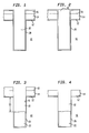
- FIG. 1 a cross-sectional view through one of the deep trenches 18 etched in a silicon substrate 10 is shown.
- the method of the present invention is implemented after a first resist fill for buried plate formation (not shown) and node dielectric 20 of SiN has been deposited in the deep trench 18 using conventional LPCVD techniques.
- the deep trench 18 is formed using conventional RIE techniques.
- a pad oxide layer 12, a SiN pad layer 14, and a deep trench mask layer 16 of TEOS have been deposited on the surface of the substrate 10.
- a second resist fill 22 of for example, AZ 7500 is deposited (without baking) in the deep trench 18 as shown in FIG. 2.
- a second CDE is used to etch the resist fill 22 to a depth D1 of approximately 1.5 um, this being the depth of a previously defined arsenosilicate glass (ASG)/buried plate (not shown).
- ASG arsenosilicate glass
- additional silicon on the order of approximately 10 nm can be removed from the upper portion of the deep trench sidewall 19 in order enlarge the deep trench 18 to account for the later growing of an oxide at the upper portion of the deep trench sidewall 19 which could hinder the proper filling of the deep trench 18 with polysilicon.
- the entire deep trench mask layer 16 of TEOS that was used for forming the deep trench 18 has been stripped away using a 7:1 BHF etch for 520s. As shown, the etching is performed without undercutting the pad films 14 and 12.
- a node reoxidation process is performed. As shown in FIG. 5, the node reoxidation process oxidizes the node dielectric 20 remaining in the deep trench 18 and grows a collar oxide 24.
- the node reoxidation process uses a thermal wet oxidation performed at approximately 900°C at 10 m wet O 2 , to grow the collar oxide 24 along the deep trench sidewall 19 to a thickness of approximately 50 nm.
- the deep trench 18 has been filled once again with a third resist fill 26 and subsequently recessed using a CDE process down to a depth D2 of between 100 and 150 nm below the surface 11 of the silicon substrate 10.
- a short duration wet etch using a 40:1 BHF (approximately 3 - 4 minutes) or alternatively a 7:1 BHF (approximately 30 - 40 seconds), has been used to remove the collar oxide 24 off the deep trench sidewall 19.
- the wet etch is used to form the lower portion of a buried strap 28.
- the resist fill 26 is cleaned from the deep trench 18.
- the deep trench 18 has been filled with an arsenic-doped polysilicon 30 which covers the pad SiN 14.
- the polysilicon fill 30 is subsequently planarized down to the pad SiN 14 using a chemical-mechanical polish as shown in FIG. 9.
- the polysilicon fill and planarization steps described above are performed only once in the method of the present invention as compared to the 3 polysilicon fills and chemical-mechanical polishes of prior art techniques.
- a buried strap recess process is performed along with the remaining process steps for a 256 Mb DRAM.
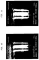
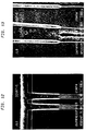
- FIGS. 12 and 13 are SEM micrographs of deep trenches that have proceeded through the following processing steps: 1) CDE to form the second recess, 2) 7:1 - 520 s BHF etch (mask TEOS strip), 3) resist clean, 4) node reoxidation (900°C - 10 m wet), and 5) intrinsic polyfill.
- FIGS. 12 and 13 show an oxide, approximately 50 nm thick, along the deep trench sidewall.
- the "bird-beak” shaped structure is important as it provides a smooth transition between the reoxidized node dielectric and the collar oxide. Thus, the probability of deep trench-substrate shorts are greatly reduced.
- the voids which can be observed in the polysilicon fill underneath the collar oxide can be minimized by slightly recessing the deep trench sidewalls as described earlier, by using the CDE after the resist/node dielectric etch, to etch off the top portion of the deep trench.
- a TEOS mask strip of approximately 9 minutes long can be implemented after performing the second CDE due to the presence of the SiN node dielectric present within the undercut region of the pad oxide.
- This undercut region is formed during the removal of the ASG which forms the buried plate.
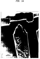
- the undercut region can vary in length from the cross-section TEMs of the pad oxide undercut, thus, the undercut region has been observed to vary as much as 70 nm.
- the node dielectric is deposited and "plugs" up the undercut region entirely.
- FIG 14 is a cross-section TEM micrograph which shows a 70nm undercut region that is, for the most part, filled entirely with the node dielectric. The presence of this node dielectric protects the pad oxide from being fully undercut and allows for further oxide etches, namely the mask TEOS etch and the collar oxide etch to define the bottom of the buried strap.
- the primary benefits of the method of the present invention are lower cost and reduced process time. In particular a cost savings of approximately 11% and a process time savings achieved through an approximately 49% reduction in the number of processing steps, are realized over the present DT processing methods.
- the method of the present invention does not require any unique tools or tool development.
- the elimination of the first and second polysilicon fills substantially avoids the possibility of oxide residuals from either incomplete collar etching, or interfacial oxide buildup of the first As-doped polysilicon fill (e.g. formed during the waiting period between the first and second polysilicon fills).
- the corresponding reduction from three DT poly CMPs to one DT poly CMP substantial overcomes or reduces the problem of pad SiN erosion due to the multiple CMPs.
- the presence of a thermally-grown oxide for the collar oxide avoids the diffusion of oxygen into the collar oxide and generally reduces the formation of the vertical bird's beak of the collar oxide. This, in turn, should reduce the tendency of trench-induced dislocations from forming in the array. Still further DT-substrate shorts are generally eliminated since the present invention produces a smooth transition from the thermally grown collar oxide to the node dielectric. Finally, the metals that are typically present in reactive ion etching (RIE) during polyfill recess processes which could adversely affect the storage capacity of the DT are substantially eliminated.
- RIE reactive ion etching
Landscapes
- Engineering & Computer Science (AREA)
- Manufacturing & Machinery (AREA)
- Semiconductor Memories (AREA)
- Semiconductor Integrated Circuits (AREA)
Applications Claiming Priority (2)
| Application Number | Priority Date | Filing Date | Title |
|---|---|---|---|
| US08/610,912 US5656535A (en) | 1996-03-04 | 1996-03-04 | Storage node process for deep trench-based DRAM |
| US610912 | 1996-03-04 |
Publications (2)
| Publication Number | Publication Date |
|---|---|
| EP0794567A2 true EP0794567A2 (de) | 1997-09-10 |
| EP0794567A3 EP0794567A3 (de) | 2000-01-12 |
Family
ID=24446904
Family Applications (1)
| Application Number | Title | Priority Date | Filing Date |
|---|---|---|---|
| EP97102901A Withdrawn EP0794567A3 (de) | 1996-03-04 | 1997-02-21 | Verfahren zur Herstellung eines Speicherknotens mit Tiefgrabenstruktur für DRAM |
Country Status (5)
| Country | Link |
|---|---|
| US (3) | US5656535A (de) |
| EP (1) | EP0794567A3 (de) |
| JP (1) | JPH09246498A (de) |
| KR (1) | KR970067886A (de) |
| TW (1) | TW375793B (de) |
Cited By (4)
| Publication number | Priority date | Publication date | Assignee | Title |
|---|---|---|---|---|
| DE19852763A1 (de) * | 1998-09-04 | 2000-05-25 | Mosel Vitelic Inc | Verfahren zur Herstellung von Graben-Kondensatoren für DRAM-Zellen |
| US9443730B2 (en) | 2014-07-18 | 2016-09-13 | Asm Ip Holding B.V. | Process for forming silicon-filled openings with a reduced occurrence of voids |
| US9837271B2 (en) | 2014-07-18 | 2017-12-05 | Asm Ip Holding B.V. | Process for forming silicon-filled openings with a reduced occurrence of voids |
| US10460932B2 (en) | 2017-03-31 | 2019-10-29 | Asm Ip Holding B.V. | Semiconductor device with amorphous silicon filled gaps and methods for forming |
Families Citing this family (56)
| Publication number | Priority date | Publication date | Assignee | Title |
|---|---|---|---|---|
| US5656535A (en) * | 1996-03-04 | 1997-08-12 | Siemens Aktiengesellschaft | Storage node process for deep trench-based DRAM |
| US6013937A (en) * | 1997-09-26 | 2000-01-11 | Siemens Aktiengesellshaft | Buffer layer for improving control of layer thickness |
| US6057216A (en) * | 1997-12-09 | 2000-05-02 | International Business Machines Corporation | Low temperature diffusion process for dopant concentration enhancement |
| US6124206A (en) * | 1997-12-29 | 2000-09-26 | Siemens Aktiengesellschaft | Reduced pad erosion |
| US6190955B1 (en) | 1998-01-27 | 2001-02-20 | International Business Machines Corporation | Fabrication of trench capacitors using disposable hard mask |
| US6066566A (en) * | 1998-01-28 | 2000-05-23 | International Business Machines Corporation | High selectivity collar oxide etch processes |
| US6107135A (en) * | 1998-02-11 | 2000-08-22 | Kabushiki Kaisha Toshiba | Method of making a semiconductor memory device having a buried plate electrode |
| US6008104A (en) * | 1998-04-06 | 1999-12-28 | Siemens Aktiengesellschaft | Method of fabricating a trench capacitor with a deposited isolation collar |
| US6310375B1 (en) * | 1998-04-06 | 2001-10-30 | Siemens Aktiengesellschaft | Trench capacitor with isolation collar and corresponding manufacturing method |
| TW471164B (en) * | 1998-06-02 | 2002-01-01 | Ibm | Deep trench-based storage capacitor and method of fabricating |
| WO1999067817A1 (en) | 1998-06-22 | 1999-12-29 | Applied Materials, Inc. | Silicon trench etching using silicon-containing precursors to reduce or avoid mask erosion |
| US6074954A (en) | 1998-08-31 | 2000-06-13 | Applied Materials, Inc | Process for control of the shape of the etch front in the etching of polysilicon |
| US6194736B1 (en) | 1998-12-17 | 2001-02-27 | International Business Machines Corporation | Quantum conductive recrystallization barrier layers |
| US6259129B1 (en) | 1999-04-20 | 2001-07-10 | International Business Machines Corporation | Strap with intrinsically conductive barrier |
| TW415010B (en) * | 1999-04-20 | 2000-12-11 | Mosel Vitelic Inc | Method for fabricating trench capacitor |
| US6236077B1 (en) | 1999-04-20 | 2001-05-22 | International Business Machines Corporation | Trench electrode with intermediate conductive barrier layer |
| US6387810B2 (en) * | 1999-06-28 | 2002-05-14 | International Business Machines Corporation | Method for homogenizing device parameters through photoresist planarization |
| US6271142B1 (en) | 1999-07-29 | 2001-08-07 | International Business Machines Corporation | Process for manufacture of trench DRAM capacitor buried plates |
| EP1077475A3 (de) * | 1999-08-11 | 2003-04-02 | Applied Materials, Inc. | Verfahren zur Mikrobearbeitung einer Körperhölung mit mehrfachem Profil |
| US6214686B1 (en) | 1999-09-01 | 2001-04-10 | International Business Machines Corporation | Spatially offset deep trenches for high density DRAMS |
| DE19956078B4 (de) * | 1999-11-22 | 2006-12-28 | Infineon Technologies Ag | Verfahren zur Herstellung eines Isolationskragens in einem Grabenkondensators |
| US6833079B1 (en) | 2000-02-17 | 2004-12-21 | Applied Materials Inc. | Method of etching a shaped cavity |
| US6415431B1 (en) | 2000-02-18 | 2002-07-02 | International Business Machines Corporation | Repair of phase shift materials to enhance adhesion |
| US6429092B1 (en) * | 2000-06-19 | 2002-08-06 | Infineon Technologies Ag | Collar formation by selective oxide deposition |
| US6417063B1 (en) | 2000-06-22 | 2002-07-09 | Infineon Technologies Richmond, Lp | Folded deep trench capacitor and method |
| US6573137B1 (en) * | 2000-06-23 | 2003-06-03 | International Business Machines Corporation | Single sided buried strap |
| DE10056256B4 (de) * | 2000-11-14 | 2004-11-25 | Promos Technologies, Inc. | Neue Technik zur Verbesserung der Kapazität eines tiefen Grabens durch dessen Oberflächenvergrößerung |
| US6451702B1 (en) * | 2001-02-16 | 2002-09-17 | International Business Machines Corporation | Methods for forming lateral trench optical detectors |
| US6518118B2 (en) | 2001-03-15 | 2003-02-11 | International Business Machines Corporation | Structure and process for buried bitline and single sided buried conductor formation |
| WO2002076666A2 (en) * | 2001-03-22 | 2002-10-03 | Xsil Technology Limited | A laser machining system and method |
| US6670235B1 (en) | 2001-08-28 | 2003-12-30 | Infineon Technologies Ag | Process flow for two-step collar in DRAM preparation |
| DE10162908B4 (de) * | 2001-12-20 | 2006-09-07 | Promos Technologies, Inc. | Verfahren zur Herstellung einer Kondensatordielektrikumsstruktur und Kondensatordielektrikumsstruktur |
| TWI291735B (en) * | 2002-01-28 | 2007-12-21 | Nanya Technology Corp | Method for forming bottle-shaped trench in semiconductor substrate |
| US6867089B2 (en) * | 2002-01-28 | 2005-03-15 | Nanya Technology Corporation | Method of forming a bottle-shaped trench in a semiconductor substrate |
| US6797636B2 (en) * | 2002-05-31 | 2004-09-28 | Infineon Technologies Ag | Process of fabricating DRAM cells with collar isolation layers |
| US6635526B1 (en) | 2002-06-07 | 2003-10-21 | Infineon Technologies Ag | Structure and method for dual work function logic devices in vertical DRAM process |
| US6905944B2 (en) * | 2003-05-08 | 2005-06-14 | International Business Machines Corporation | Sacrificial collar method for improved deep trench processing |
| US6838334B1 (en) | 2003-07-30 | 2005-01-04 | International Business Machines Corporation | Method of fabricating a buried collar |
| KR100529632B1 (ko) * | 2003-10-01 | 2005-11-17 | 동부아남반도체 주식회사 | 반도체 소자 및 그 제조 방법 |
| US6974991B2 (en) * | 2003-10-29 | 2005-12-13 | International Business Machines Corp. | DRAM cell with buried collar and self-aligned buried strap |
| US7276751B2 (en) * | 2005-09-09 | 2007-10-02 | International Business Machines Corporation | Trench metal-insulator-metal (MIM) capacitors integrated with middle-of-line metal contacts, and method of fabricating same |
| KR100707803B1 (ko) * | 2005-10-28 | 2007-04-17 | 주식회사 하이닉스반도체 | 리세스 게이트를 갖는 반도체 소자의 제조방법 |
| US7410862B2 (en) * | 2006-04-28 | 2008-08-12 | International Business Machines Corporation | Trench capacitor and method for fabricating the same |
| US7375413B2 (en) * | 2006-05-26 | 2008-05-20 | International Business Machines Corporation | Trench widening without merging |
| WO2008094529A1 (en) * | 2007-01-29 | 2008-08-07 | Jeffrey Jacob Cernohous | Compositions and methods for producing high strength composites |
| US7846791B2 (en) * | 2007-11-08 | 2010-12-07 | International Business Machines Corporation | Structure for a trench capacitor |
| US20100240190A1 (en) * | 2009-03-19 | 2010-09-23 | United Microelectronics Corp. | Method for fabricating deep trench capacitor |
| US8021945B2 (en) * | 2009-04-14 | 2011-09-20 | International Business Machines Corporation | Bottle-shaped trench capacitor with enhanced capacitance |
| US8227311B2 (en) | 2010-10-07 | 2012-07-24 | International Business Machines Corporation | Method of forming enhanced capacitance trench capacitor |
| US9837254B2 (en) | 2014-08-12 | 2017-12-05 | Lam Research Corporation | Differentially pumped reactive gas injector |
| US9406535B2 (en) | 2014-08-29 | 2016-08-02 | Lam Research Corporation | Ion injector and lens system for ion beam milling |
| US10825652B2 (en) | 2014-08-29 | 2020-11-03 | Lam Research Corporation | Ion beam etch without need for wafer tilt or rotation |
| US9536748B2 (en) * | 2014-10-21 | 2017-01-03 | Lam Research Corporation | Use of ion beam etching to generate gate-all-around structure |
| US9779955B2 (en) | 2016-02-25 | 2017-10-03 | Lam Research Corporation | Ion beam etching utilizing cryogenic wafer temperatures |
| KR20250011246A (ko) | 2019-02-28 | 2025-01-21 | 램 리써치 코포레이션 | 측벽 세정을 사용한 이온 빔 에칭 |
| US12334345B2 (en) * | 2021-05-27 | 2025-06-17 | Fujian Jinhua Integrated Circuit Co., Ltd. | Dynamic random access memory device with active regions of different profile roughness and method for forming the same |
Family Cites Families (29)
| Publication number | Priority date | Publication date | Assignee | Title |
|---|---|---|---|---|
| US3943047A (en) * | 1974-05-10 | 1976-03-09 | Bell Telephone Laboratories, Incorporated | Selective removal of material by sputter etching |
| US4016062A (en) * | 1975-09-11 | 1977-04-05 | International Business Machines Corporation | Method of forming a serrated surface topography |
| US4128765A (en) * | 1976-10-29 | 1978-12-05 | Joseph Franks | Ion beam machining techniques and apparatus |
| CA1053627A (en) * | 1976-12-09 | 1979-05-01 | Bonar And Bemis Ltd. | Automatic wicketted bag loader |
| US4214966A (en) * | 1979-03-20 | 1980-07-29 | Bell Telephone Laboratories, Incorporated | Process useful in the fabrication of articles with metallized surfaces |
| US4309267A (en) * | 1980-07-21 | 1982-01-05 | Bell Telephone Laboratories, Incorporated | Reactive sputter etching apparatus |
| US4502913A (en) * | 1982-06-30 | 1985-03-05 | International Business Machines Corporation | Total dielectric isolation for integrated circuits |
| JPS59208749A (ja) * | 1983-05-12 | 1984-11-27 | Nec Corp | 半導体装置の製造方法 |
| US5225697A (en) * | 1984-09-27 | 1993-07-06 | Texas Instruments, Incorporated | dRAM cell and method |
| JPS62125680A (ja) * | 1985-11-26 | 1987-06-06 | Nec Corp | 半導体装置の製造方法 |
| US4801988A (en) * | 1986-10-31 | 1989-01-31 | International Business Machines Corporation | Semiconductor trench capacitor cell with merged isolation and node trench construction |
| DE3851649T2 (de) * | 1987-03-20 | 1995-05-04 | Nippon Electric Co | Aus einer Vielzahl von Eintransistorzellen bestehende dynamische Speichervorrichtung mit wahlfreiem Zugriff. |
| JPH01149572A (ja) * | 1987-12-05 | 1989-06-12 | Toshiba Corp | 画像読取装置 |
| JPH01149957A (ja) * | 1987-12-07 | 1989-06-13 | Hitachi Ltd | 薄膜形成装置および薄膜形成方法 |
| US5205902A (en) * | 1989-08-18 | 1993-04-27 | Galileo Electro-Optics Corporation | Method of manufacturing microchannel electron multipliers |
| JP2932650B2 (ja) * | 1990-09-17 | 1999-08-09 | 松下電器産業株式会社 | 微細構造物の製造方法 |
| US5096849A (en) * | 1991-04-29 | 1992-03-17 | International Business Machines Corporation | Process for positioning a mask within a concave semiconductor structure |
| JPH06163851A (ja) * | 1991-06-07 | 1994-06-10 | Texas Instr Japan Ltd | 半導体装置及びその製造方法 |
| US5422294A (en) * | 1993-05-03 | 1995-06-06 | Noble, Jr.; Wendell P. | Method of making a trench capacitor field shield with sidewall contact |
| JP3480745B2 (ja) * | 1993-09-16 | 2003-12-22 | 株式会社東芝 | 半導体装置の製造方法 |
| US5360758A (en) * | 1993-12-03 | 1994-11-01 | International Business Machines Corporation | Self-aligned buried strap for trench type DRAM cells |
| US5395786A (en) * | 1994-06-30 | 1995-03-07 | International Business Machines Corporation | Method of making a DRAM cell with trench capacitor |
| US5658816A (en) * | 1995-02-27 | 1997-08-19 | International Business Machines Corporation | Method of making DRAM cell with trench under device for 256 Mb DRAM and beyond |
| US5525531A (en) * | 1995-06-05 | 1996-06-11 | International Business Machines Corporation | SOI DRAM with field-shield isolation |
| US5692281A (en) * | 1995-10-19 | 1997-12-02 | International Business Machines Corporation | Method for making a dual trench capacitor structure |
| US5827765A (en) * | 1996-02-22 | 1998-10-27 | Siemens Aktiengesellschaft | Buried-strap formation in a dram trench capacitor |
| US5656535A (en) * | 1996-03-04 | 1997-08-12 | Siemens Aktiengesellschaft | Storage node process for deep trench-based DRAM |
| US5717628A (en) * | 1996-03-04 | 1998-02-10 | Siemens Aktiengesellschaft | Nitride cap formation in a DRAM trench capacitor |
| US5937296A (en) * | 1996-12-20 | 1999-08-10 | Siemens Aktiengesellschaft | Memory cell that includes a vertical transistor and a trench capacitor |
-
1996
- 1996-03-04 US US08/610,912 patent/US5656535A/en not_active Expired - Fee Related
-
1997
- 1997-01-21 US US08/784,558 patent/US5849638A/en not_active Expired - Fee Related
- 1997-02-21 EP EP97102901A patent/EP0794567A3/de not_active Withdrawn
- 1997-02-27 TW TW086102394A patent/TW375793B/zh not_active IP Right Cessation
- 1997-03-03 KR KR1019970006875A patent/KR970067886A/ko not_active Withdrawn
- 1997-03-04 JP JP9063929A patent/JPH09246498A/ja active Pending
-
1998
- 1998-07-01 US US09/108,619 patent/US6153474A/en not_active Expired - Lifetime
Cited By (5)
| Publication number | Priority date | Publication date | Assignee | Title |
|---|---|---|---|---|
| DE19852763A1 (de) * | 1998-09-04 | 2000-05-25 | Mosel Vitelic Inc | Verfahren zur Herstellung von Graben-Kondensatoren für DRAM-Zellen |
| DE19852763B4 (de) * | 1998-09-04 | 2004-04-29 | Mosel Vitelic Inc. | Verfahren zur Herstellung eines Graben-Kondensators |
| US9443730B2 (en) | 2014-07-18 | 2016-09-13 | Asm Ip Holding B.V. | Process for forming silicon-filled openings with a reduced occurrence of voids |
| US9837271B2 (en) | 2014-07-18 | 2017-12-05 | Asm Ip Holding B.V. | Process for forming silicon-filled openings with a reduced occurrence of voids |
| US10460932B2 (en) | 2017-03-31 | 2019-10-29 | Asm Ip Holding B.V. | Semiconductor device with amorphous silicon filled gaps and methods for forming |
Also Published As
| Publication number | Publication date |
|---|---|
| US5849638A (en) | 1998-12-15 |
| TW375793B (en) | 1999-12-01 |
| JPH09246498A (ja) | 1997-09-19 |
| US5656535A (en) | 1997-08-12 |
| EP0794567A3 (de) | 2000-01-12 |
| KR970067886A (ko) | 1997-10-13 |
| US6153474A (en) | 2000-11-28 |
Similar Documents
| Publication | Publication Date | Title |
|---|---|---|
| US5656535A (en) | Storage node process for deep trench-based DRAM | |
| US5933748A (en) | Shallow trench isolation process | |
| KR100343353B1 (ko) | 트렌치 캐패시터 구조체 및 그 제조 방법 | |
| US6177698B1 (en) | Formation of controlled trench top isolation layers for vertical transistors | |
| EP0656655B1 (de) | Selbstausgerichtes vergrabenes Band für DRAM Grabenzellen | |
| US6359299B1 (en) | Apparatus and method for forming controlled deep trench top isolation layers | |
| EP1198832B1 (de) | Verfahren zur herstellung einer vergrabenen verbindung für einen grabenkondensator | |
| US6703273B2 (en) | Aggressive capacitor array cell layout for narrow diameter DRAM trench capacitor structures via SOI technology | |
| US6069058A (en) | Shallow trench isolation for semiconductor devices | |
| US6967136B2 (en) | Method and structure for improved trench processing | |
| JPS62269335A (ja) | 半導体デバイスの製造方法 | |
| JPH11145275A (ja) | シャロートレンチ分離構造及びその形成方法 | |
| US6509226B1 (en) | Process for protecting array top oxide | |
| US6040213A (en) | Polysilicon mini spacer for trench buried strap formation | |
| US6420750B1 (en) | Structure and method for buried-strap with reduced outdiffusion | |
| US6358785B1 (en) | Method for forming shallow trench isolation structures | |
| US6677197B2 (en) | High aspect ratio PBL SiN barrier formation | |
| JP2004523918A (ja) | 半導体メモリセルおよびその製造方法 | |
| US6964898B1 (en) | Method for fabricating deep trench capacitor | |
| US6403492B1 (en) | Method of manufacturing semiconductor devices with trench isolation | |
| KR100204023B1 (ko) | 반도체 장치의 소자분리막 형성방법 | |
| EP0949674A2 (de) | Verfahren zur Herstellung eines vergrabenen Verbindungsstreifens für einen Grabenkondensator | |
| KR20020003018A (ko) | 실리콘 라이너를 이용한 트렌치 소자분리방법 | |
| KR910002012B1 (ko) | 휘발성 메모리 소자의 제조방법 | |
| HK1030096A (en) | Formation of controlled trench top isolation layers for vertical transistors |
Legal Events
| Date | Code | Title | Description |
|---|---|---|---|
| PUAI | Public reference made under article 153(3) epc to a published international application that has entered the european phase |
Free format text: ORIGINAL CODE: 0009012 |
|
| AK | Designated contracting states |
Kind code of ref document: A2 Designated state(s): DE FR GB IT |
|
| PUAL | Search report despatched |
Free format text: ORIGINAL CODE: 0009013 |
|
| AK | Designated contracting states |
Kind code of ref document: A3 Designated state(s): DE FR GB IT |
|
| RIC1 | Information provided on ipc code assigned before grant |
Free format text: 7H 01L 21/8242 A, 7H 01L 27/108 B, 7H 01L 21/70 B |
|
| 17P | Request for examination filed |
Effective date: 20000619 |
|
| RAP1 | Party data changed (applicant data changed or rights of an application transferred) |
Owner name: INTERNATIONAL BUSINESS MACHINES CORPORATION Owner name: INFINEON TECHNOLOGIES AG |
|
| 17Q | First examination report despatched |
Effective date: 20070323 |
|
| STAA | Information on the status of an ep patent application or granted ep patent |
Free format text: STATUS: THE APPLICATION IS DEEMED TO BE WITHDRAWN |
|
| 18D | Application deemed to be withdrawn |
Effective date: 20090901 |