EP0794677A2 - Procédé et circuit pour la séparation des signaux de luminance et de chrominance dans un signal composite de couleur - Google Patents
Procédé et circuit pour la séparation des signaux de luminance et de chrominance dans un signal composite de couleur Download PDFInfo
- Publication number
- EP0794677A2 EP0794677A2 EP97103172A EP97103172A EP0794677A2 EP 0794677 A2 EP0794677 A2 EP 0794677A2 EP 97103172 A EP97103172 A EP 97103172A EP 97103172 A EP97103172 A EP 97103172A EP 0794677 A2 EP0794677 A2 EP 0794677A2
- Authority
- EP
- European Patent Office
- Prior art keywords
- signals
- values
- signal
- lines
- distance
- Prior art date
- Legal status (The legal status is an assumption and is not a legal conclusion. Google has not performed a legal analysis and makes no representation as to the accuracy of the status listed.)
- Granted
Links
Images


Classifications
-
- H—ELECTRICITY
- H04—ELECTRIC COMMUNICATION TECHNIQUE
- H04N—PICTORIAL COMMUNICATION, e.g. TELEVISION
- H04N9/00—Details of colour television systems
- H04N9/77—Circuits for processing the brightness signal and the chrominance signal relative to each other, e.g. adjusting the phase of the brightness signal relative to the colour signal, correcting differential gain or differential phase
- H04N9/78—Circuits for processing the brightness signal and the chrominance signal relative to each other, e.g. adjusting the phase of the brightness signal relative to the colour signal, correcting differential gain or differential phase for separating the brightness signal or the chrominance signal from the colour television signal, e.g. using comb filter
Definitions
- the invention relates to a method and a circuit arrangement for separating luminance and chrominance signals of a CVBS signal, in particular a comb filter arrangement for PAL signals.
- the transmitted CVBS signal consists of luminance and chrominance signals.
- the chrominance signal in turn is composed of two color difference signals (U / V signals for PAL, I / Q signals for NTSC), which are modulated on a color carrier in the quadrature phase.
- Comb filters are used for this purpose, which, on the basis of line, field and picture delays for signal separation, link several adjacent lines. It is customary to work with an image content-dependent control which, depending on how the chrominance signals are structured, switches between different filter algorithms.
- the invention has for its object to provide a method for separating luminance and chrominance signals of a composite signal, in particular to prevent the occurrence of cross effects, such as. B. to minimize the so-called "hanging dots" comb filter errors. This object is achieved by the method specified in claim 1.
- the invention is based on the further object of specifying a circuit arrangement for separating luminance and chrominance signals of a CVBS signal. This object is achieved by the circuit arrangement specified in claim 6.
- the method according to the invention for separating luminance and chrominance signals of a CVBS signal by linking several image lines, in which a link is selected from various links, is first to demodulate two color component signals from the CVBS signal are evaluated together with the CVBS signal to determine the link to be selected and then a luminance signal and color difference signals are generated by the selected link.
- the color component signals in addition to the color difference signals also containing the high-frequency component of the luminance signals.
- both the CVBS signal and the color component signals are each delayed by a whole number of lines and by twice this number, and the high-frequency component of the CVBS signal and the color component signals of three non-, single- and double-delayed lines are delayed by one Weighting according to the optimal link generates the chrominance signals as well as the high-frequency luminance signals of the single delay line.
- the chrominance signals can be averaged over several lines and the low-frequency component of the single-delayed CVBS signal added to the high-frequency luminance signal.
- the circuit arrangement according to the invention consists in that a demodulator is provided which demodulates two color component signals from the composite signal, which together with the composite signal are fed to a comb filter, in which these signals are first evaluated to determine the link to be selected and then a luminance signal and color difference signals are generated by the selected link.
- line memories are advantageously provided in the comb filter in order to delay both the CVBS signal and the color component signals. Furthermore, the CVBS and color component signals of the differently delayed lines are fed to a decision logic and one or more switching and averaging blocks, in which the chrominance signals and the high-frequency luminance signals are generated.
- the CVBS signal fed to the comb filter is preferably broken down into a high and a low pass component by a high-pass / low-pass combination and only the high-pass component is fed to the switching and averaging block, and the low-pass component to the decision logic.
- the generated chrominance signals are preferably supplied with median filters which average the chrominance signals over several lines, and on the other hand an adder can be provided in order to add the low-frequency component of the simply delayed CVBS signal to the generated high-frequency luminance signal.
- the decision logic has a first block, to which the differently delayed lines are fed, different distance, difference and sum signals being calculated from the supplied signals, these values being compared with preselected values or other calculated values and depending on decision signals are determined from the comparison result, and the decision signals are fed to a second block in which, for each combination of the decision signals, one or more decision values are determined which are fed to the switching and averaging blocks for actuation.
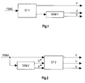
- Fig. 1 the arrangement of a conventional comb filter is shown.
- the FBAS signal FBAS is first fed to the comb filter CF1.
- This comb filter then splits the FBAS signal FBAS into a luminance signal Y and a chrominance signal that is still to be demodulated.
- the chrominance signal is then fed to a demodulator DEM1, in which the color difference signals U and V are regenerated.
- the algorithm selection is based only on an evaluation of the high-frequency signal components.
- the comb filter according to the invention is arranged as shown in FIG. 2.
- the FBAS signal FBAS is first fed to a demodulator DEM2.
- the color component signals U * and V * generated by this demodulator DEM2, like the FBAS signal FBAS, are then fed to the comb filter CF2.
- Comb filter CF2 then removes the carried chrominance signal components from the composite signal and removes the demodulated high-frequency luminance signals erroneously contained therein from color component signals U * and V *.
- the comb filter CF2 therefore processes demodulated chrominance signals in contrast to conventional comb filters.
- the separated luminance and color difference signals Y, U, V are then available at the output of the comb filter.
- FIG. 3 shows a block diagram of the comb filter CF2 according to the invention, a link of three lines being used as an example for the line comb filtering.
- the CVBS signal FBAS and the U * and V * signals are each delayed in two delay stages D1, D2 or D3, D4 or D5, D6.
- Line memories in particular FIFO memories, are preferably used for this.
- the differently delayed CVBS signals are then initially with a High-low-pass combination LHF1, LHF2 or LHF3 broken down into the respective high-pass component HPa, HPc, HPe and low-pass component LPa, LPc, LPe.
- Both the low-pass signals LPa, LPc, LPe and the demodulated chrominance signals Ua, Uc, Ue and Va, Vc, Ve of the differently delayed lines are then fed to a logic block FM.
- This block analyzes which patterns the signals have.
- the decision signals CM, LM, XC1 to XC5 are then assigned specific values and fed to the block DM.
- this block e.g. B. in table form, for the possible combinations of the decision signals, two decision values CD and LD are stored. The decision values are used to control the switching and averaging blocks for the luminance and chrominance signals.
- the low-frequency luminance component LPc is then added to the output signal of this block with the aid of an adder AL.
- blocks SC1 and SC2 are followed by averaging over several lines by means of a median filter M1 and M2, which can have line memories for delaying the color difference signals. This averaging eliminates switching artifacts that can be caused by noise in particular.
- FIG. 4 shows a block diagram of the logic block FM.
- the differently delayed lines are fed to the decision logic, different distance, difference and sum signals being calculated from the supplied signals. These values are then compared to preselected values or other calculated values. Different decision signals are then determined depending on the respective comparison result.
- a first distance value dac, dce or dae is determined for every two image lines, which corresponds to the distance between the color signals of the two lines given by the two color component signals U *, V *.
- These first distance values are then compared with preselected values or first distance values for another line combination or a fraction of these first distance values.
- block 4 it is checked whether the distance values dac, dce and dae are all smaller than a predetermined barrier with the value "15". If this is the case, the decision signal CM is assigned the value "0". If, on the other hand, at least one of the distance values lies above the predetermined barrier, the distance values are fed to the next comparison block 5. Depending on the structure of the chrominance signals, ie the result of the comparisons carried out by blocks 4 to 9, the decision signal CM thus has one of the values between "0" and "6".
- blocks 10 to 15 are used to make comparisons for difference values which result for the low-pass components of two picture lines each.
- a second decision signal LM is then assigned a value between "0" and "6", which reflects the structure in the luminance component of the examined image lines.
- further distance values are also determined in block 16.
- the distance values decs and dacs thus give the distance between the sum of the color signals of lines e and c or a and c from the origin. These distance values are compared with half the distance of the color signal of line c from the origin dc. It is also checked whether the distance from c to the origin dc is either less than a quarter of the distances da and de or greater than four times the distances da and de. Depending on these comparison results, the decision signals XC1, XC2 and XC3 are each assigned either the value "0" or "1".
- are used for the color component signals and (
- ) / 8 are calculated and again compared with one another or with a specific threshold value in order to give the decision signals XC4, XC5 a binary value assign.
- luminance and chrominance signals generally have different sampling frequencies (4: 1: 1).
- an adjustment could, for. B. done by performing a 4: 1 up-conversion of the chrominance signals before the comb filter.
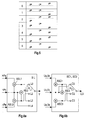
- the image signal modes corresponding to the decision signals CM and LM are illustrated in FIG. 5.
- mode 0 the values of all three lines are within a barrier and therefore close together.
- line e differs significantly from lines a and c, i.e. there is an edge. Accordingly, there is also an edge in mode 2, because line a differs significantly from lines c and e.
- mode 3 line a is between lines c and e, in mode 4 line e is between lines a and c.
- all lines are approximately in a line, in mode 6 in a zigzag.
- the result values CM, LM, XC1 - XC5 are evaluated in the block DM. It will be for every combination of the two Decision signals CM and LM decided how the chrominance signals and high-pass luminance signals are to be processed. For this purpose, the decision values CD and LD are determined, which are given in Tables 1 and 2, whereby for some CM / LM combinations two decision values are possible which depend on the current binary value of a further decision signal XC1 to XC5.
- the switching and averaging blocks SL and SC1, SC2 are controlled with the decision values CD and LD. Block diagrams of these two blocks are shown in Figures 6 a) and b).
- the high-frequency luminance signal components HPa, HPc, HPe of lines a, c and e are supplied to block SL.
- various combinations of the luminance signals are then calculated.
- These links are present at the outputs L1 - L4.
- a 0 signal is generated, ie only the low-pass luminance signal LPc is reproduced by the comb filter. This leads to a loss of sharpness, but it can completely eliminate ink residue that cannot be reduced by combining it with other lines.
- the block SC1 or SC2 from FIG. 6b is constructed in a very similar manner.
- the color component signals Ua, Va, Uc, Vc, Ue, Ve are present on the block and, by means of a link using the adders ASC1-ASC3, corresponding chrominance signals are available at the outputs C0-C3.
- the invention can be integrated in whole or in part in an integrated circuit, but can also be implemented in whole or in part by software.
- the invention can e.g. B. for PAL and NTSC television systems, but also for further developments of these systems. An application is particularly possible with PALplus receivers.
Landscapes
- Engineering & Computer Science (AREA)
- Multimedia (AREA)
- Signal Processing (AREA)
- Processing Of Color Television Signals (AREA)
Applications Claiming Priority (2)
| Application Number | Priority Date | Filing Date | Title |
|---|---|---|---|
| DE19609193 | 1996-03-09 | ||
| DE19609193A DE19609193A1 (de) | 1996-03-09 | 1996-03-09 | Verfahren und Schaltungsanordnung zum Trennen von Luminanz- und Chrominanzsignalen eines FBAS-Signals |
Publications (3)
| Publication Number | Publication Date |
|---|---|
| EP0794677A2 true EP0794677A2 (fr) | 1997-09-10 |
| EP0794677A3 EP0794677A3 (fr) | 1997-09-24 |
| EP0794677B1 EP0794677B1 (fr) | 2004-04-21 |
Family
ID=7787739
Family Applications (1)
| Application Number | Title | Priority Date | Filing Date |
|---|---|---|---|
| EP97103172A Expired - Lifetime EP0794677B1 (fr) | 1996-03-09 | 1997-02-27 | Procédé et circuit pour la séparation des signaux de luminance et de chrominance dans un signal composite de couleur |
Country Status (5)
| Country | Link |
|---|---|
| US (1) | US5973753A (fr) |
| EP (1) | EP0794677B1 (fr) |
| JP (1) | JPH09331545A (fr) |
| CN (1) | CN1112054C (fr) |
| DE (2) | DE19609193A1 (fr) |
Families Citing this family (9)
| Publication number | Priority date | Publication date | Assignee | Title |
|---|---|---|---|---|
| JP2000069502A (ja) * | 1998-08-24 | 2000-03-03 | Sony Corp | 映像信号処理回路及びそれを用いた撮像装置 |
| US6771321B2 (en) * | 2001-11-06 | 2004-08-03 | Broadcom Corporation | Method and system for performing PAL luma two line vertical combing |
| CN100477807C (zh) * | 2004-01-17 | 2009-04-08 | 深圳创维-Rgb电子有限公司 | 高清电视超级处理器及方法 |
| CN100486342C (zh) * | 2004-09-09 | 2009-05-06 | 凌阳科技股份有限公司 | 可抑制假色杂讯的三维视频混成信号解调方法及系统 |
| KR100688519B1 (ko) * | 2005-01-13 | 2007-03-02 | 삼성전자주식회사 | 필드 기반의 적응적 시공간 y/c 분리를 위한 디지털영상 신호 처리 장치 및 방법 |
| KR100674939B1 (ko) * | 2005-01-13 | 2007-01-26 | 삼성전자주식회사 | 프레임 기반의 적응적 시공간 y/c 분리를 위한 디지털영상 신호 처리 장치 및 방법 |
| CN101340597B (zh) * | 2007-07-06 | 2010-12-15 | 晨星半导体股份有限公司 | 影像处理方法及影像处理装置 |
| US8237863B2 (en) * | 2008-01-12 | 2012-08-07 | Huaya Microelectronics | Adaptive gain and offset control in a digital video decoder |
| CN102026004B (zh) * | 2009-09-10 | 2013-01-30 | 联咏科技股份有限公司 | 影像色彩处理元件与方法 |
Family Cites Families (15)
| Publication number | Priority date | Publication date | Assignee | Title |
|---|---|---|---|---|
| US3591707A (en) * | 1969-01-08 | 1971-07-06 | Gen Electric | Color television demodulator |
| US3946431A (en) * | 1974-10-01 | 1976-03-23 | Basf Aktiengesellschaft | Synchronized demodulation of the chrominance signal with switched carrier phase angles |
| JPS5760791A (en) * | 1980-09-30 | 1982-04-12 | Toshiba Corp | Demodulating circuit for wide-band receiving chrominance |
| US4573068A (en) * | 1984-03-21 | 1986-02-25 | Rca Corporation | Video signal processor for progressive scanning |
| GB8509306D0 (en) * | 1985-04-11 | 1985-05-15 | British Broadcasting Corp | Pal decoders |
| US4893176A (en) * | 1985-10-09 | 1990-01-09 | Faroudja Y C | Adaptive comb filter for quadrature modulated color television systems |
| GB8622680D0 (en) * | 1986-09-19 | 1986-10-22 | Robinson R N | Decoder |
| GB2223142B (en) * | 1988-09-23 | 1993-01-06 | Sony Corp | Separating components of composite digital video signals |
| DE3931903C2 (de) * | 1989-09-25 | 1994-10-27 | Broadcast Television Syst | Verfahren und Schaltung zur Signaltrennung eines PAL-Signals |
| JP3263791B2 (ja) * | 1992-09-30 | 2002-03-11 | ソニー株式会社 | Yc分離回路 |
| EP0613311A1 (fr) * | 1993-02-26 | 1994-08-31 | Kabushiki Kaisha Toshiba | Circuit de séparation Y/C |
| US5347321A (en) * | 1993-09-30 | 1994-09-13 | Texas Instruments Incorporated | Color separator for digital television |
| KR0157480B1 (ko) * | 1994-06-18 | 1998-11-16 | 김광호 | 화상처리에서 에지방향에 적응하는 휘도신호와 색신호 분리방법 및 회로 |
| US5424784A (en) * | 1994-09-06 | 1995-06-13 | Raytheon Company | Method and apparatus for cross fading between combed and simple filtered outputs |
| JPH0998291A (ja) * | 1995-07-26 | 1997-04-08 | Nec Eng Ltd | 自動サンプリング装置 |
-
1996
- 1996-03-09 DE DE19609193A patent/DE19609193A1/de not_active Withdrawn
-
1997
- 1997-02-10 US US08/797,913 patent/US5973753A/en not_active Expired - Lifetime
- 1997-02-27 CN CN97103405A patent/CN1112054C/zh not_active Expired - Fee Related
- 1997-02-27 DE DE59711526T patent/DE59711526D1/de not_active Expired - Lifetime
- 1997-02-27 EP EP97103172A patent/EP0794677B1/fr not_active Expired - Lifetime
- 1997-03-06 JP JP9051869A patent/JPH09331545A/ja active Pending
Also Published As
| Publication number | Publication date |
|---|---|
| DE19609193A1 (de) | 1997-09-11 |
| US5973753A (en) | 1999-10-26 |
| CN1112054C (zh) | 2003-06-18 |
| JPH09331545A (ja) | 1997-12-22 |
| CN1164804A (zh) | 1997-11-12 |
| EP0794677B1 (fr) | 2004-04-21 |
| EP0794677A3 (fr) | 1997-09-24 |
| DE59711526D1 (de) | 2004-05-27 |
Similar Documents
| Publication | Publication Date | Title |
|---|---|---|
| DE69622614T2 (de) | Verfahren zur adaptiven Fehlerdiffusion | |
| DE3226038C2 (de) | Filterschaltung | |
| DE2810697C2 (de) | Verfahren zur Trennung des Farbartsignals vom Leuchtdichtesignal bei Farbfernsehsignalen mit quadraturmodulierten Farbhilfsträgern | |
| DE3784769T2 (de) | Videosignal-verarbeitungsschaltungen. | |
| DE3842977C2 (de) | Mischeinrichtung für Videosignale | |
| DE3821398C2 (de) | Verfahren und Einrichtung zum Trennen von Leuchtdichte- und Farbsignal eines Farbfernsehsignalgemisches | |
| DE3234938C2 (fr) | ||
| DE4039558C2 (de) | Helligkeitssignal/Farbsignal-Weiche für ein Farbfernsehsignal | |
| EP0344579B1 (fr) | Dispositif de réduction du bruit et de la diaphonie couleur dans les signaux de télévision | |
| EP0794677B1 (fr) | Procédé et circuit pour la séparation des signaux de luminance et de chrominance dans un signal composite de couleur | |
| DE3842978C2 (de) | Mischeinrichtung für Videosignale | |
| DE69928576T2 (de) | Luminanz- und Chrominanz-Trennschaltung | |
| DE69405276T2 (de) | Kammfilter zur Reduzierung von Cross Color-Phänomenen und -Geräuschen | |
| DE3786581T2 (de) | Kodierung und dekodierung von digitalen videokomponentensignalen. | |
| DE4124698C2 (fr) | ||
| DE69026441T2 (de) | Adaptive Kammfilter und Verfahren zum Trennen von Videosignal-Komponenten | |
| DE69323947T2 (de) | Luminanz-/Chrominanzsignaltrennschaltungen | |
| DE19523438A1 (de) | Verfahren zur Einblendung eines Hintergrund-Bildsignals in Teile eines Vordergrund-Bildsignals und Schaltung zur Durchführung dieses Verfahrens | |
| DE3152649C2 (fr) | ||
| DE4142782A1 (de) | Variable chrominanz-filterung zur kodierung von tv-signalen | |
| DE69714638T2 (de) | 2-Linien-Y/C-Trennschaltung | |
| DE3639733A1 (de) | Anordnung zur verschaerfung vertikaler bildfeinheiten fuer ein video-wiedergabesystem | |
| DE68908911T2 (de) | Schaltung zur Trennung des Helligkeitssignals von einem Farbsignal. | |
| EP0501558B1 (fr) | Dispositif de séparation d'un signal d'image couleur en un signal de couleur et un signal de luminance | |
| DE3930806C2 (fr) |
Legal Events
| Date | Code | Title | Description |
|---|---|---|---|
| PUAI | Public reference made under article 153(3) epc to a published international application that has entered the european phase |
Free format text: ORIGINAL CODE: 0009012 |
|
| PUAL | Search report despatched |
Free format text: ORIGINAL CODE: 0009013 |
|
| AK | Designated contracting states |
Kind code of ref document: A2 Designated state(s): DE FR GB IT |
|
| AK | Designated contracting states |
Kind code of ref document: A3 Designated state(s): DE FR GB IT |
|
| 17P | Request for examination filed |
Effective date: 19980221 |
|
| 17Q | First examination report despatched |
Effective date: 20020618 |
|
| GRAP | Despatch of communication of intention to grant a patent |
Free format text: ORIGINAL CODE: EPIDOSNIGR1 |
|
| GRAS | Grant fee paid |
Free format text: ORIGINAL CODE: EPIDOSNIGR3 |
|
| GRAA | (expected) grant |
Free format text: ORIGINAL CODE: 0009210 |
|
| AK | Designated contracting states |
Kind code of ref document: B1 Designated state(s): DE FR GB IT |
|
| REG | Reference to a national code |
Ref country code: GB Ref legal event code: FG4D Free format text: NOT ENGLISH |
|
| GBT | Gb: translation of ep patent filed (gb section 77(6)(a)/1977) |
Effective date: 20040421 |
|
| REF | Corresponds to: |
Ref document number: 59711526 Country of ref document: DE Date of ref document: 20040527 Kind code of ref document: P |
|
| ET | Fr: translation filed | ||
| PLBE | No opposition filed within time limit |
Free format text: ORIGINAL CODE: 0009261 |
|
| STAA | Information on the status of an ep patent application or granted ep patent |
Free format text: STATUS: NO OPPOSITION FILED WITHIN TIME LIMIT |
|
| REG | Reference to a national code |
Ref country code: FR Ref legal event code: D6 |
|
| 26N | No opposition filed |
Effective date: 20050124 |
|
| PGFP | Annual fee paid to national office [announced via postgrant information from national office to epo] |
Ref country code: FR Payment date: 20110310 Year of fee payment: 15 Ref country code: IT Payment date: 20110219 Year of fee payment: 15 Ref country code: DE Payment date: 20110217 Year of fee payment: 15 |
|
| PGFP | Annual fee paid to national office [announced via postgrant information from national office to epo] |
Ref country code: GB Payment date: 20110225 Year of fee payment: 15 |
|
| GBPC | Gb: european patent ceased through non-payment of renewal fee |
Effective date: 20120227 |
|
| REG | Reference to a national code |
Ref country code: FR Ref legal event code: ST Effective date: 20121031 |
|
| PG25 | Lapsed in a contracting state [announced via postgrant information from national office to epo] |
Ref country code: IT Free format text: LAPSE BECAUSE OF NON-PAYMENT OF DUE FEES Effective date: 20120227 |
|
| REG | Reference to a national code |
Ref country code: DE Ref legal event code: R119 Ref document number: 59711526 Country of ref document: DE Effective date: 20120901 |
|
| PG25 | Lapsed in a contracting state [announced via postgrant information from national office to epo] |
Ref country code: GB Free format text: LAPSE BECAUSE OF NON-PAYMENT OF DUE FEES Effective date: 20120227 Ref country code: FR Free format text: LAPSE BECAUSE OF NON-PAYMENT OF DUE FEES Effective date: 20120229 |
|
| PG25 | Lapsed in a contracting state [announced via postgrant information from national office to epo] |
Ref country code: DE Free format text: LAPSE BECAUSE OF NON-PAYMENT OF DUE FEES Effective date: 20120901 |