EP0797375B1 - Dispositif organique électroluminescent contenant de nouveaux matériaux transportant des trous de charge - Google Patents
Dispositif organique électroluminescent contenant de nouveaux matériaux transportant des trous de charge Download PDFInfo
- Publication number
- EP0797375B1 EP0797375B1 EP97103641A EP97103641A EP0797375B1 EP 0797375 B1 EP0797375 B1 EP 0797375B1 EP 97103641 A EP97103641 A EP 97103641A EP 97103641 A EP97103641 A EP 97103641A EP 0797375 B1 EP0797375 B1 EP 0797375B1
- Authority
- EP
- European Patent Office
- Prior art keywords
- group
- hole transporting
- layer
- organic
- carbon atoms
- Prior art date
- Legal status (The legal status is an assumption and is not a legal conclusion. Google has not performed a legal analysis and makes no representation as to the accuracy of the status listed.)
- Expired - Lifetime
Links
- 0 *c1cc(*(c2ccccc2)c(cc2)ccc2N(c2ccc(*(c3ccccc3)c3cccc(N)c3)cc2)c(cc2)ccc2N(c2ccccc2)c2cc(N)ccc2)ccc1 Chemical compound *c1cc(*(c2ccccc2)c(cc2)ccc2N(c2ccc(*(c3ccccc3)c3cccc(N)c3)cc2)c(cc2)ccc2N(c2ccccc2)c2cc(N)ccc2)ccc1 0.000 description 6
- JOEYCSZZZHZTKJ-UHFFFAOYSA-N Cc1cccc(N(c2ccccc2)c2ccc(-c(cc3)c(CCC=C4)c4c3N(c3ccccc3)c3cccc(C)c3)c3c2cccc3)c1 Chemical compound Cc1cccc(N(c2ccccc2)c2ccc(-c(cc3)c(CCC=C4)c4c3N(c3ccccc3)c3cccc(C)c3)c3c2cccc3)c1 JOEYCSZZZHZTKJ-UHFFFAOYSA-N 0.000 description 1
Images

Classifications
-
- H—ELECTRICITY
- H05—ELECTRIC TECHNIQUES NOT OTHERWISE PROVIDED FOR
- H05B—ELECTRIC HEATING; ELECTRIC LIGHT SOURCES NOT OTHERWISE PROVIDED FOR; CIRCUIT ARRANGEMENTS FOR ELECTRIC LIGHT SOURCES, IN GENERAL
- H05B33/00—Electroluminescent light sources
- H05B33/12—Light sources with substantially two-dimensional [2D] radiating surfaces
- H05B33/14—Light sources with substantially two-dimensional [2D] radiating surfaces characterised by the chemical or physical composition or the arrangement of the electroluminescent material, or by the simultaneous addition of the electroluminescent material in or onto the light source
-
- C—CHEMISTRY; METALLURGY
- C07—ORGANIC CHEMISTRY
- C07C—ACYCLIC OR CARBOCYCLIC COMPOUNDS
- C07C211/00—Compounds containing amino groups bound to a carbon skeleton
- C07C211/43—Compounds containing amino groups bound to a carbon skeleton having amino groups bound to carbon atoms of six-membered aromatic rings of the carbon skeleton
- C07C211/57—Compounds containing amino groups bound to a carbon skeleton having amino groups bound to carbon atoms of six-membered aromatic rings of the carbon skeleton having amino groups bound to carbon atoms of six-membered aromatic rings being part of condensed ring systems of the carbon skeleton
- C07C211/58—Naphthylamines; N-substituted derivatives thereof
-
- H—ELECTRICITY
- H05—ELECTRIC TECHNIQUES NOT OTHERWISE PROVIDED FOR
- H05B—ELECTRIC HEATING; ELECTRIC LIGHT SOURCES NOT OTHERWISE PROVIDED FOR; CIRCUIT ARRANGEMENTS FOR ELECTRIC LIGHT SOURCES, IN GENERAL
- H05B33/00—Electroluminescent light sources
- H05B33/12—Light sources with substantially two-dimensional [2D] radiating surfaces
-
- H—ELECTRICITY
- H10—SEMICONDUCTOR DEVICES; ELECTRIC SOLID-STATE DEVICES NOT OTHERWISE PROVIDED FOR
- H10K—ORGANIC ELECTRIC SOLID-STATE DEVICES
- H10K50/00—Organic light-emitting devices
- H10K50/10—OLEDs or polymer light-emitting diodes [PLED]
- H10K50/11—OLEDs or polymer light-emitting diodes [PLED] characterised by the electroluminescent [EL] layers
-
- H—ELECTRICITY
- H10—SEMICONDUCTOR DEVICES; ELECTRIC SOLID-STATE DEVICES NOT OTHERWISE PROVIDED FOR
- H10K—ORGANIC ELECTRIC SOLID-STATE DEVICES
- H10K85/00—Organic materials used in the body or electrodes of devices covered by this subclass
- H10K85/60—Organic compounds having low molecular weight
- H10K85/615—Polycyclic condensed aromatic hydrocarbons, e.g. anthracene
- H10K85/626—Polycyclic condensed aromatic hydrocarbons, e.g. anthracene containing more than one polycyclic condensed aromatic rings, e.g. bis-anthracene
-
- H—ELECTRICITY
- H10—SEMICONDUCTOR DEVICES; ELECTRIC SOLID-STATE DEVICES NOT OTHERWISE PROVIDED FOR
- H10K—ORGANIC ELECTRIC SOLID-STATE DEVICES
- H10K85/00—Organic materials used in the body or electrodes of devices covered by this subclass
- H10K85/60—Organic compounds having low molecular weight
- H10K85/631—Amine compounds having at least two aryl rest on at least one amine-nitrogen atom, e.g. triphenylamine
- H10K85/633—Amine compounds having at least two aryl rest on at least one amine-nitrogen atom, e.g. triphenylamine comprising polycyclic condensed aromatic hydrocarbons as substituents on the nitrogen atom
-
- H—ELECTRICITY
- H10—SEMICONDUCTOR DEVICES; ELECTRIC SOLID-STATE DEVICES NOT OTHERWISE PROVIDED FOR
- H10K—ORGANIC ELECTRIC SOLID-STATE DEVICES
- H10K85/00—Organic materials used in the body or electrodes of devices covered by this subclass
- H10K85/30—Coordination compounds
Definitions
- This invention relates to an organic electroluminescence device and, more specifically, to a device with a new hole transporting material.
- Organic electroluminescent (EL) devices are generally composed of three layers of organic molecules sandwiched between transparent and metallic electrodes, the three layers including an electron transporting layer, an emissive layer and a hole transporting layer.
- Organic EL devices are attractive owing to low driving voltage and a potential application to full color flat emissive displays. Though significant lifetime has been achieved in the prior art (See US Patent No. 4,720,432, entitled “Electroluminescent Device with Organic Luminescent Medium", issued January 19, 1988), further improvement is needed for applications where high brightness is required.
- the hole transporting materials used in the hole transporting zone of an organic EL device are the most vulnerable parts which are susceptible to thermal degradation by physical aggregation or recrystallization.
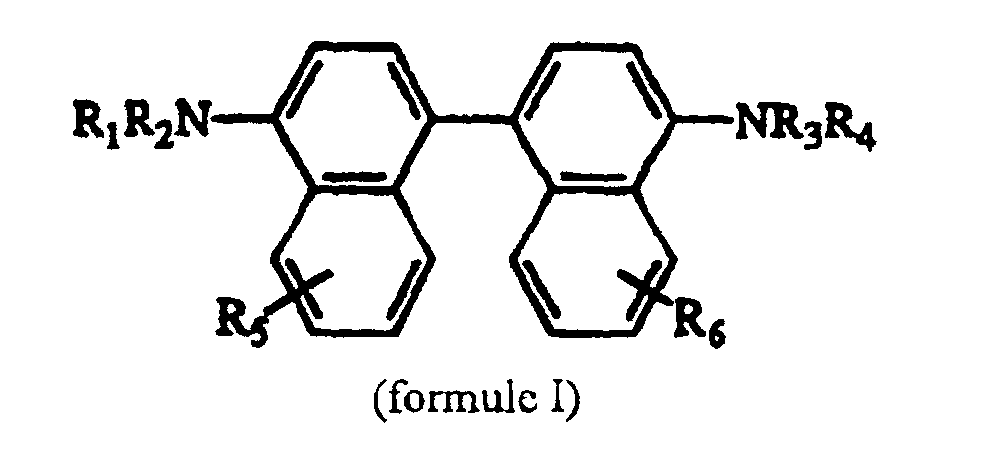
- An organic EL device comprises a cathode, an electron transporting layer, an emitting layer, a hole transporting layer and an anode which are laminated in sequence, where said hole transporting layer is made of a substance represented by the following chemical formula I: where R 1 ,R 2 ,R 3 ,R 4 ,R 5 ,R 6 each independently represent a hydrogen atom, an alkyl group of from 1 to 6 carbon atoms, a halogen group, a cyano group, a nitro group, or an aryl group of from 6 to 15 carbon atoms, a fused aromatic group, an alkoxy group, an alkylamine group, an aryloxy group, or an arylamine group.
- R 1 ,R 2 ,R 3 ,R 4 ,R 5 ,R 6 each independently represent a hydrogen atom, an alkyl group of from 1 to 6 carbon atoms, a halogen group, a cyano group, a nitro group, or an aryl group
- the single figure is a simplified cross-sectional view of a light emitting diode in accordance with the present invention.
- the present invention is directed to an organic light emitting device which, in general, consists of thin layers of organic molecules sandwiched between transparent and metallic electrodes.
- Organic LED 10 includes a transparent substrate 11 which in this specific embodiment is a glass or plastic plate having a relatively planar upper surface.
- a transparent electrically conductive layer 12 is deposited on the planar surface of substrate 11 so as to form a relatively uniform electrical contact.
- a hole transporting layer 13 made of organic hole transporting materials is deposited on the surface of conductive layer 12.
- An emissive organic layer 14 made of a host emissive material containing a guest fluorescent dopant is deposited onto the surface of layer 13.
- an electron transporting layer 15 made of an electron transporting material is deposited on the surface of layer 14 and a second electrically conductive layer 16 is deposited on the upper surface of layer 15 to form a second electrical contact.
- conductive layer 16 is formed of any of a wide range of metals or alloys in which at least one metal has a work function less than 4.0 eV.
- the work functions of the materials making up layers 15 and 16 are substantially matched to reduce the required operating voltage and improve the efficiency of organic LED 10. Additional information on work function matching is disclosed in a copending U.S. Patent Application entitled “Organic LED with Improved Efficiency", filed 12 September 1994, bearing serial number 08/304,454, and assigned to the same assignee.
- conductive layer 12 is a p-type contact and conductive layer 16 is an n-type contact.
- the negative terminal of a potential source 17 is connected to conductive layer 16 and the positive terminal is connected to conductive layer 12.
- a potential is applied between layers 12 and 16 by means of potential source 17
- electrons injected from the n-type contact (layer 16) are transported through organic layer 15 and into organic layer 14 (the emissive layer) and holes injected from the p-type contact (layer 12) are transported through organic layer 13 and into organic layer 14 (the emissive layer), where upon an electron and a hole recombination a photon is emitted.
- the hole transporting materials made up of tertiary aromatic amines are the least thermally stable materials in organic electroluminescent devices. Especially, when an organic EL device is driven at high electric current density, the hole transporting materials in the hole transporting layer tend to aggregate or reorganize to form islands, domains and pinholes. The change in film uniformity and homogeneity of hole transporting materials causes initially the gradual degradation in device luminance and eventually the device failure.
- the glass transition temperature (Tg) of a material is an indicator for thermal stability of the resulting amorphous films.
- Higher glass transition temperature offers higher thermal stability for an amorphous film.
- a large molecule weight and strong steric hindrance to stacking are two of the main factors that determine tie glass transition temperature of an organic material.
- an organic EL device as illustrated in LED 10 comprises a cathode, an electron transporting layer, an emitting layer, a hole transporting layer and an anode which are laminated in sequence, where said hole transporting layer is made of a substance with central binaphthyl group represented by the following chemical formula: where R 1 ,R 2 ,R 3 ,R 4 ,R 5 ,R 6 each independently represent a hydrogen atom, an alkyl group of from 1 to 6 carbon atoms, a halogen group, a cyano group, a nitro group, or an aryl group of from 6 to 15 carbon atoms, a fused aromatic group, an alkoxy group, an alkylamine group, an aryloxy group, or an arylamine group.
- R 1 ,R 2 ,R 3 ,R 4 ,R 5 ,R 6 each independently represent a hydrogen atom, an alkyl group of from 1 to 6 carbon atoms, a halogen group, a cyano
- the hole transporting material used in the hole transporting layer in organic EL device 10 has glass transition temperatures above 75 oC. However, it is preferred that hole transporting material having glass transition temperature greater then 90 oC is to be used to achieve a long lasting organic EL device.
- the hole transporting layer in LED 10 is composed of two layers of hole transporting materials, wherein, at least one layer of the hole transporting material is selected from the substance represent by formula I in accordance with the present invention.
- the hole transporting layer in LED 10 is composed of a layer of mixed hole transporting materials, wherein, at least one of the hole transporting materials is selected from the substance represented by formula I in accordance with present invention.
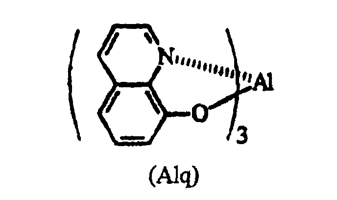
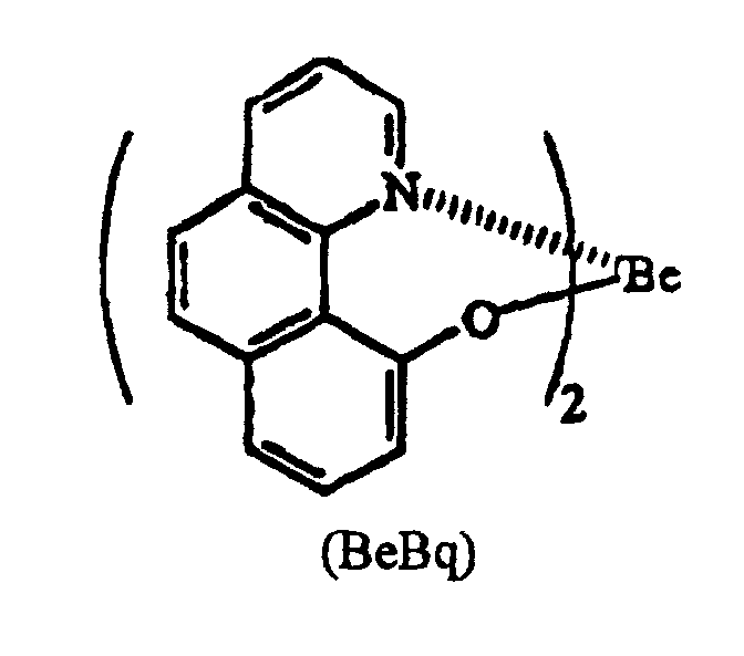
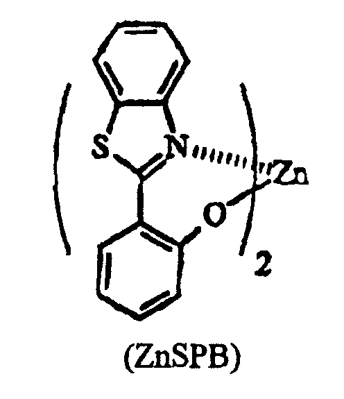
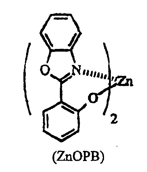
- the electron transporting layer 15 of LED 10 is preferred to, but not limited to, be selected from the following electron transporting materials:
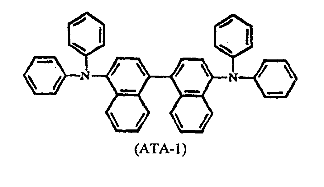
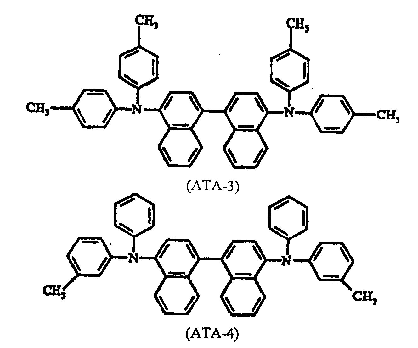
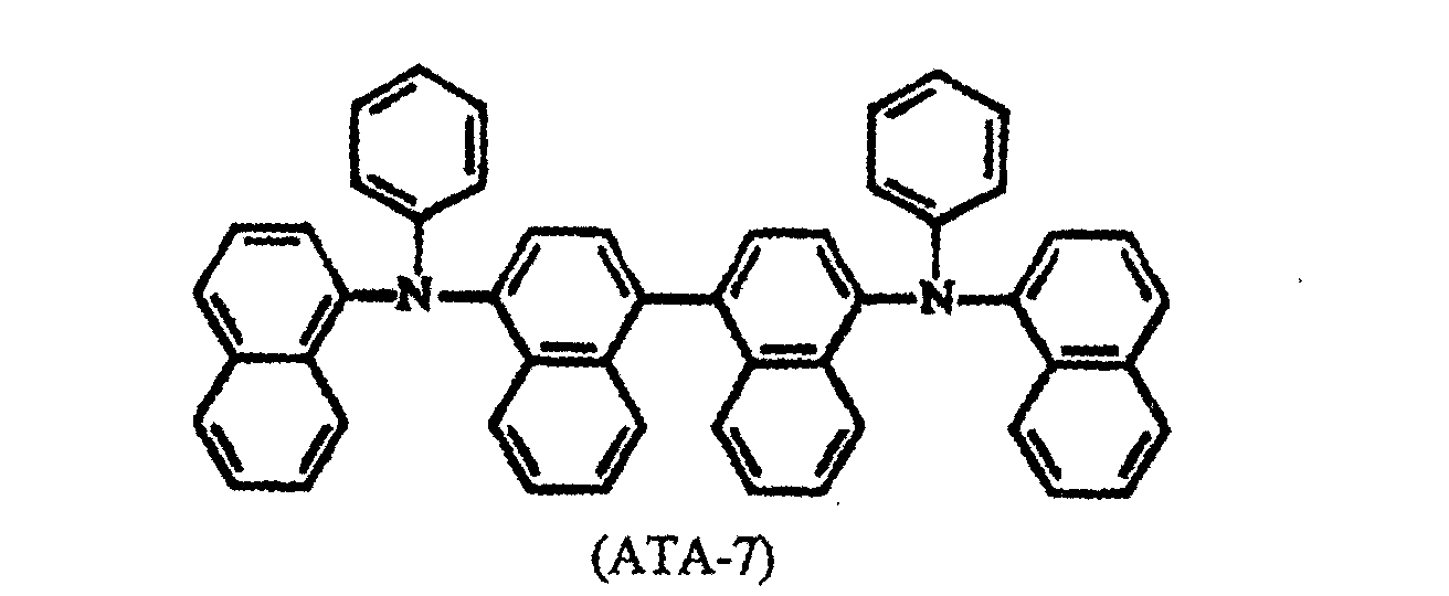
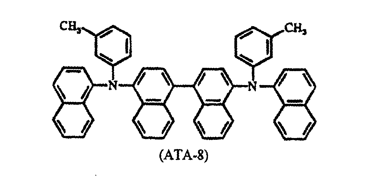
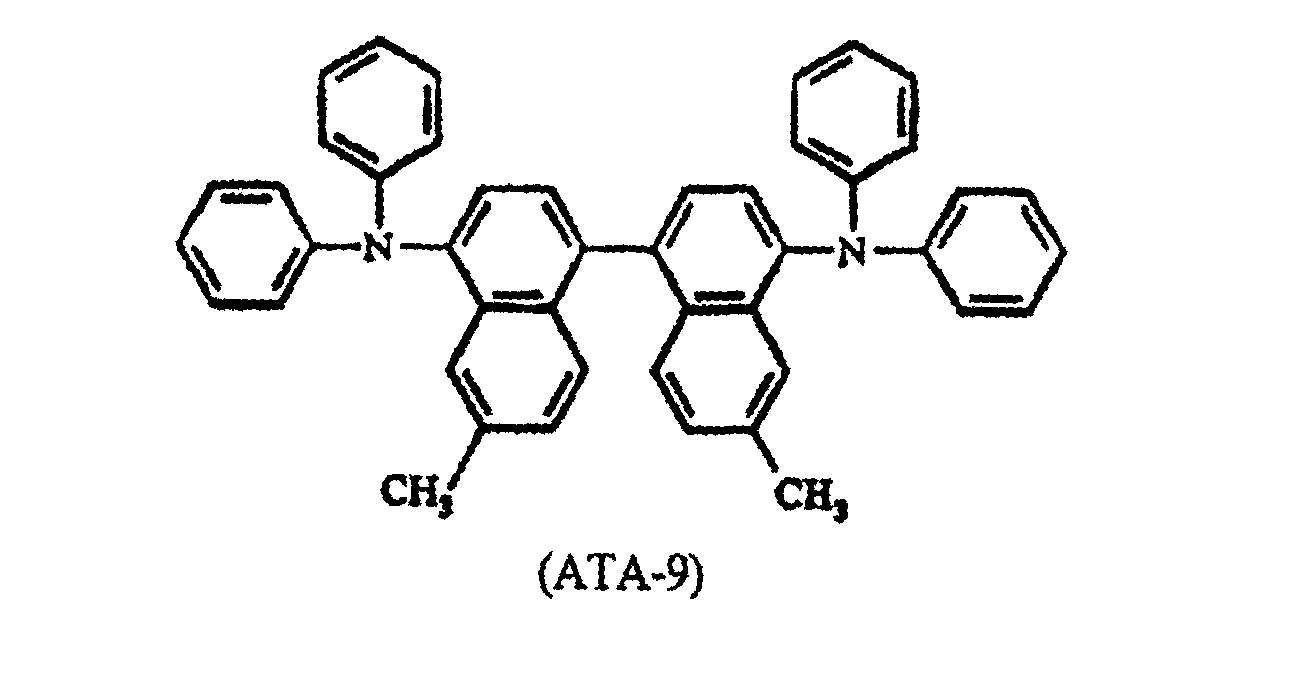
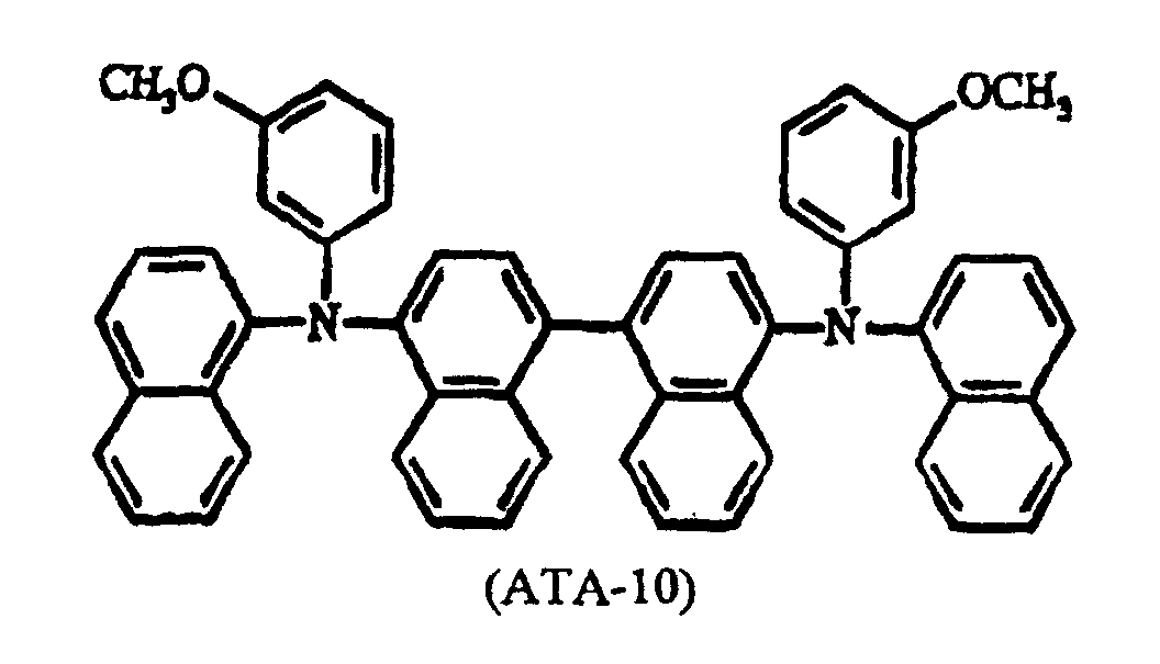
- the hole transporting materials used in the embodied organic EL device generally have high glass transition temperatures because of the rigid central binaphthyl group. Since higher glass transition temperature generally renders higher thermal stability for an amorphous film, the organic EL devices according to the present invention provide better reliability under high current density driving condition then normal organic EL devices.
Landscapes
- Chemical & Material Sciences (AREA)
- Physics & Mathematics (AREA)
- Organic Chemistry (AREA)
- Spectroscopy & Molecular Physics (AREA)
- Engineering & Computer Science (AREA)
- Materials Engineering (AREA)
- Optics & Photonics (AREA)
- Electroluminescent Light Sources (AREA)
- Luminescent Compositions (AREA)
Claims (6)
- Dispositif électroluminescent organique comprenant une cathode (16), une couche de transport d'électrons (15), une couche émettrice (14), une couche de transport de trous (13) et une anode (12), stratifiées dans cet ordre, dans lequel ladite couche de transport de trous (13) comprend un matériau représenté par la formule chimique I suivante:dans laquelle R1, R2, R3, R4, R5 et R6 représentent chacun indépendamment un atome d'hydrogène, un groupe alkyle de 1 à 6 atomes de carbone, un groupe halogéno, un groupe cyano, un groupe nitro, un groupe aryle de 6 à 15 atomes de carbone, un groupe aromatique condensé, un groupe alcoxy, un groupe alkylamino, un groupe aryloxy ou un groupe arylamino.

- Dispositif électroluminescent organique selon la revendication 1, dans lequel le matériau de transport de trous (13) a une température de transition vitreuse supérieure à 75°C.
- Dispositif électroluminescent organique selon la revendication 1, dans lequel le matériau de transport de trous (13) est choisi parmi les matériaux suivants:




- Dispositif électroluminescent organique selon la revendication 1, dans lequel la couche de transport d'électrons (15) est composée de l'un des matériaux suivants:
- Dispositif électroluminescent organique selon la revendication 1, dans lequel la couche de transport de trous (13) comprend deux couches de matériaux de transport de trous et au moins une couche de matériau de transport de trous est choisie parmi les substances représentées par la formule I suivante:dans laquelle R1, R2, R3, R4, R5 et R6 représentent chacun indépendamment un atome d'hydrogène, un groupe alkyle de 1 à 6 atomes de carbone, un groupe halogéno, un groupe cyano, un groupe nitro, un groupe aryle de 6 à 15 atomes de carbone, un groupe aromatique condensé, un groupe alcoxy, un groupe alkylamino, un groupe aryloxy ou un groupe arylamino.
- Dispositif électroluminescent organique selon la revendication 1, dans lequci la couche de transport de trous (13) comprend une couche de matériaux de transport de trous mélangés, au moins un des matériaux de transport de trous étant choisi parmi les substances représentées par la formule I suivante :dans laquelle R1, R2, R3, R4, R5 et R6 représentent chacun indépendamment un atome d'hydrogène, un groupe alkyle de 1 à 6 atomes de carbone, un groupe halogéno, un groupe cyano, un groupe nitro, un groupe aryle de 6 à 15 atomes de carbone, un groupe aromatique condensé, un groupe alcoxy, un groupe alkylamino, un groupe aryloxy ou un groupe arylamino.

Applications Claiming Priority (2)
| Application Number | Priority Date | Filing Date | Title |
|---|---|---|---|
| US61683396A | 1996-03-19 | 1996-03-19 | |
| US616833 | 1996-03-19 |
Publications (3)
| Publication Number | Publication Date |
|---|---|
| EP0797375A2 EP0797375A2 (fr) | 1997-09-24 |
| EP0797375A3 EP0797375A3 (fr) | 1998-03-11 |
| EP0797375B1 true EP0797375B1 (fr) | 2002-06-05 |
Family
ID=24471118
Family Applications (1)
| Application Number | Title | Priority Date | Filing Date |
|---|---|---|---|
| EP97103641A Expired - Lifetime EP0797375B1 (fr) | 1996-03-19 | 1997-03-05 | Dispositif organique électroluminescent contenant de nouveaux matériaux transportant des trous de charge |
Country Status (4)
| Country | Link |
|---|---|
| EP (1) | EP0797375B1 (fr) |
| JP (1) | JP4215837B2 (fr) |
| DE (1) | DE69712961T2 (fr) |
| TW (1) | TW365104B (fr) |
Families Citing this family (17)
| Publication number | Priority date | Publication date | Assignee | Title |
|---|---|---|---|---|
| JPH09279134A (ja) * | 1996-04-11 | 1997-10-28 | Shinko Electric Ind Co Ltd | 有機el素子 |
| JP3985311B2 (ja) * | 1997-10-20 | 2007-10-03 | チッソ株式会社 | アミン誘導体及びそれを用いた有機電界発光素子 |
| JP4545243B2 (ja) * | 1997-12-16 | 2010-09-15 | チッソ株式会社 | ジアミノナフタレン誘導体、及びそれを用いた有機電界発光素子 |
| JP2956691B1 (ja) | 1998-05-22 | 1999-10-04 | 日本電気株式会社 | 有機エレクトロルミネッセンス素子 |
| US6465116B1 (en) | 1998-06-08 | 2002-10-15 | Nec Corporation | Organic electroluminescent device |
| US6699594B1 (en) | 1998-06-08 | 2004-03-02 | Nec Corporation | Organic electroluminescent device |
| US6656608B1 (en) * | 1998-12-25 | 2003-12-02 | Konica Corporation | Electroluminescent material, electroluminescent element and color conversion filter |
| KR100377321B1 (ko) * | 1999-12-31 | 2003-03-26 | 주식회사 엘지화학 | 피-형 반도체 성질을 갖는 유기 화합물을 포함하는 전기소자 |
| US7560175B2 (en) | 1999-12-31 | 2009-07-14 | Lg Chem, Ltd. | Electroluminescent devices with low work function anode |
| KR100721656B1 (ko) | 2005-11-01 | 2007-05-23 | 주식회사 엘지화학 | 유기 전기 소자 |
| DE60138790D1 (de) | 2000-09-25 | 2009-07-09 | Konica Corp | Organisches Elektrolumineszenzelement und dafür verwendetes organisches Elektrolumineszenzmaterial |
| US6872475B2 (en) * | 2002-12-03 | 2005-03-29 | Canon Kabushiki Kaisha | Binaphthalene derivatives for organic electro-luminescent devices |
| US20040142206A1 (en) * | 2003-01-17 | 2004-07-22 | Bazan Guillermo C. | Binaphthol based chromophores for the fabrication of blue organic light emitting diodes |
| EP1794255B1 (fr) | 2004-08-19 | 2016-11-16 | LG Chem, Ltd. | Dispositif lumineux organique comprenant une couche tampon et procede de fabrication correspondant |
| KR100645085B1 (ko) * | 2004-12-22 | 2006-11-10 | 네오뷰코오롱 주식회사 | 아릴아민계 유기 반도체 화합물 및 이를 포함하는 유기발광 다이오드 |
| JP4832017B2 (ja) * | 2005-04-25 | 2011-12-07 | ケミプロ化成株式会社 | ビナフチル誘導体、それよりなるホスト材料、ホール輸送材料およびそれを用いた有機el素子 |
| US8680693B2 (en) | 2006-01-18 | 2014-03-25 | Lg Chem. Ltd. | OLED having stacked organic light-emitting units |
Family Cites Families (3)
| Publication number | Priority date | Publication date | Assignee | Title |
|---|---|---|---|---|
| JP3272189B2 (ja) * | 1994-10-18 | 2002-04-08 | 京セラミタ株式会社 | ナフチレンジアミン誘導体とそれを用いた電子写真感光体 |
| US5554450A (en) * | 1995-03-08 | 1996-09-10 | Eastman Kodak Company | Organic electroluminescent devices with high thermal stability |
| US5804322A (en) * | 1995-11-17 | 1998-09-08 | Motorola, Inc. | Organic electroluminescence device with mixed hole transporting materials |
-
1997
- 1997-02-12 TW TW086101551A patent/TW365104B/zh not_active IP Right Cessation
- 1997-03-05 EP EP97103641A patent/EP0797375B1/fr not_active Expired - Lifetime
- 1997-03-05 DE DE69712961T patent/DE69712961T2/de not_active Expired - Lifetime
- 1997-03-18 JP JP08443397A patent/JP4215837B2/ja not_active Expired - Fee Related
Also Published As
| Publication number | Publication date |
|---|---|
| JP4215837B2 (ja) | 2009-01-28 |
| DE69712961D1 (de) | 2002-07-11 |
| JPH09255948A (ja) | 1997-09-30 |
| TW365104B (en) | 1999-07-21 |
| DE69712961T2 (de) | 2002-11-07 |
| EP0797375A3 (fr) | 1998-03-11 |
| EP0797375A2 (fr) | 1997-09-24 |
Similar Documents
| Publication | Publication Date | Title |
|---|---|---|
| EP0774883B1 (fr) | Dispositif organique électroluminescent contenant un mélange de matériaux transportant des trous de charge | |
| EP0797375B1 (fr) | Dispositif organique électroluminescent contenant de nouveaux matériaux transportant des trous de charge | |
| JP4818494B2 (ja) | 有機elデバイス | |
| US5853905A (en) | Efficient single layer electroluminescent device | |
| EP1072669A2 (fr) | Dispositif organique électroluminescent | |
| US6495274B1 (en) | Organic electroluminescent device | |
| EP0997058A1 (fr) | Electrode a couches pelliculaires destinee a des dispositifs organiques emetteurs de lumiere, et procede de production associe | |
| JPH11144866A (ja) | 発光素子 | |
| KR100683050B1 (ko) | 유기 전계발광 장치 | |
| US6312838B1 (en) | Organic electroluminescent device | |
| CN100380701C (zh) | 有机电致发光器件 | |
| JPH11144867A (ja) | 発光素子 | |
| US6410167B2 (en) | Organic electroluminescent device | |
| US6338910B1 (en) | Organic electroluminescent device | |
| KR100581639B1 (ko) | 유기 전계발광 소자 | |
| US6194089B1 (en) | Organic electroluminescent device with improved reliability | |
| KR100826439B1 (ko) | 유기 전계발광 소자 | |
| US6555254B1 (en) | Organic electroluminescent device | |
| KR100816643B1 (ko) | 유기 전계발광 소자 | |
| JPH05335084A (ja) | 発光素子 | |
| JP2000003787A (ja) | 有機電界発光素子 | |
| JPH05311164A (ja) | 有機電界発光素子 | |
| JPH06200242A (ja) | 有機薄膜発光素子 |
Legal Events
| Date | Code | Title | Description |
|---|---|---|---|
| PUAI | Public reference made under article 153(3) epc to a published international application that has entered the european phase |
Free format text: ORIGINAL CODE: 0009012 |
|
| AK | Designated contracting states |
Kind code of ref document: A2 Designated state(s): DE FR GB |
|
| PUAL | Search report despatched |
Free format text: ORIGINAL CODE: 0009013 |
|
| AK | Designated contracting states |
Kind code of ref document: A3 Designated state(s): DE FR GB |
|
| 17P | Request for examination filed |
Effective date: 19980911 |
|
| GRAG | Despatch of communication of intention to grant |
Free format text: ORIGINAL CODE: EPIDOS AGRA |
|
| 17Q | First examination report despatched |
Effective date: 20010220 |
|
| GRAG | Despatch of communication of intention to grant |
Free format text: ORIGINAL CODE: EPIDOS AGRA |
|
| GRAH | Despatch of communication of intention to grant a patent |
Free format text: ORIGINAL CODE: EPIDOS IGRA |
|
| GRAH | Despatch of communication of intention to grant a patent |
Free format text: ORIGINAL CODE: EPIDOS IGRA |
|
| GRAA | (expected) grant |
Free format text: ORIGINAL CODE: 0009210 |
|
| AK | Designated contracting states |
Kind code of ref document: B1 Designated state(s): DE FR GB |
|
| REG | Reference to a national code |
Ref country code: GB Ref legal event code: FG4D |
|
| REF | Corresponds to: |
Ref document number: 69712961 Country of ref document: DE Date of ref document: 20020711 |
|
| ET | Fr: translation filed | ||
| PLBE | No opposition filed within time limit |
Free format text: ORIGINAL CODE: 0009261 |
|
| STAA | Information on the status of an ep patent application or granted ep patent |
Free format text: STATUS: NO OPPOSITION FILED WITHIN TIME LIMIT |
|
| 26N | No opposition filed |
Effective date: 20030306 |
|
| REG | Reference to a national code |
Ref country code: FR Ref legal event code: CD |
|
| REG | Reference to a national code |
Ref country code: DE Ref legal event code: R082 Ref document number: 69712961 Country of ref document: DE Representative=s name: SCHUMACHER & WILLSAU PATENTANWALTSGESELLSCHAFT, DE |
|
| REG | Reference to a national code |
Ref country code: DE Ref legal event code: R082 Ref document number: 69712961 Country of ref document: DE Representative=s name: SCHUMACHER & WILLSAU PATENTANWALTSGESELLSCHAFT, DE Effective date: 20110727 Ref country code: DE Ref legal event code: R081 Ref document number: 69712961 Country of ref document: DE Owner name: UNIVERSAL DISPLAY CORP., EWING, US Free format text: FORMER OWNER: MOTOROLA, INC., SCHAUMBURG, ILL., US Effective date: 20110727 |
|
| REG | Reference to a national code |
Ref country code: GB Ref legal event code: 732E Free format text: REGISTERED BETWEEN 20111117 AND 20111123 |
|
| REG | Reference to a national code |
Ref country code: FR Ref legal event code: TP Owner name: UNIVERSAL DISPLAY CORPORATION, US Effective date: 20111123 |
|
| PGFP | Annual fee paid to national office [announced via postgrant information from national office to epo] |
Ref country code: FR Payment date: 20130405 Year of fee payment: 17 Ref country code: DE Payment date: 20130327 Year of fee payment: 17 Ref country code: GB Payment date: 20130327 Year of fee payment: 17 |
|
| REG | Reference to a national code |
Ref country code: DE Ref legal event code: R119 Ref document number: 69712961 Country of ref document: DE |
|
| GBPC | Gb: european patent ceased through non-payment of renewal fee |
Effective date: 20140305 |
|
| REG | Reference to a national code |
Ref country code: FR Ref legal event code: ST Effective date: 20141128 |
|
| REG | Reference to a national code |
Ref country code: DE Ref legal event code: R119 Ref document number: 69712961 Country of ref document: DE Effective date: 20141001 |
|
| PG25 | Lapsed in a contracting state [announced via postgrant information from national office to epo] |
Ref country code: FR Free format text: LAPSE BECAUSE OF NON-PAYMENT OF DUE FEES Effective date: 20140331 Ref country code: GB Free format text: LAPSE BECAUSE OF NON-PAYMENT OF DUE FEES Effective date: 20140305 Ref country code: DE Free format text: LAPSE BECAUSE OF NON-PAYMENT OF DUE FEES Effective date: 20141001 |