EP0798507B1 - Dispositif d'éclairage de surface et affichage à cristaux liquides - Google Patents
Dispositif d'éclairage de surface et affichage à cristaux liquides Download PDFInfo
- Publication number
- EP0798507B1 EP0798507B1 EP97201696A EP97201696A EP0798507B1 EP 0798507 B1 EP0798507 B1 EP 0798507B1 EP 97201696 A EP97201696 A EP 97201696A EP 97201696 A EP97201696 A EP 97201696A EP 0798507 B1 EP0798507 B1 EP 0798507B1
- Authority
- EP
- European Patent Office
- Prior art keywords
- light
- guide plate
- light guide
- distribution
- edge
- Prior art date
- Legal status (The legal status is an assumption and is not a legal conclusion. Google has not performed a legal analysis and makes no representation as to the accuracy of the status listed.)
- Expired - Lifetime
Links
- 238000005286 illumination Methods 0.000 title claims description 92
- 239000004973 liquid crystal related substance Substances 0.000 title claims description 89
- 238000009792 diffusion process Methods 0.000 claims description 90
- 238000009826 distribution Methods 0.000 claims description 82
- 238000000034 method Methods 0.000 claims description 17
- 238000004519 manufacturing process Methods 0.000 description 8
- BQCADISMDOOEFD-UHFFFAOYSA-N Silver Chemical compound [Ag] BQCADISMDOOEFD-UHFFFAOYSA-N 0.000 description 5
- 230000015556 catabolic process Effects 0.000 description 5
- 230000003247 decreasing effect Effects 0.000 description 5
- 239000000463 material Substances 0.000 description 5
- 229910052709 silver Inorganic materials 0.000 description 5
- 239000004332 silver Substances 0.000 description 5
- 230000000694 effects Effects 0.000 description 4
- XAGFODPZIPBFFR-UHFFFAOYSA-N aluminium Chemical compound [Al] XAGFODPZIPBFFR-UHFFFAOYSA-N 0.000 description 3
- 229910052782 aluminium Inorganic materials 0.000 description 3
- 230000007423 decrease Effects 0.000 description 3
- 230000015572 biosynthetic process Effects 0.000 description 2
- 238000006243 chemical reaction Methods 0.000 description 2
- 238000010276 construction Methods 0.000 description 2
- 238000005755 formation reaction Methods 0.000 description 2
- 238000010438 heat treatment Methods 0.000 description 2
- 125000006850 spacer group Chemical group 0.000 description 2
- 239000004925 Acrylic resin Substances 0.000 description 1
- 229920000178 Acrylic resin Polymers 0.000 description 1
- 239000003086 colorant Substances 0.000 description 1
- 230000001419 dependent effect Effects 0.000 description 1
- 230000008021 deposition Effects 0.000 description 1
- 229910003460 diamond Inorganic materials 0.000 description 1
- 239000010432 diamond Substances 0.000 description 1
- 238000005530 etching Methods 0.000 description 1
- 239000011521 glass Substances 0.000 description 1
- 230000020169 heat generation Effects 0.000 description 1
- 230000003116 impacting effect Effects 0.000 description 1
- 230000010365 information processing Effects 0.000 description 1
- 238000002347 injection Methods 0.000 description 1
- 239000007924 injection Substances 0.000 description 1
- 238000003754 machining Methods 0.000 description 1
- 239000002985 plastic film Substances 0.000 description 1
- 239000004417 polycarbonate Substances 0.000 description 1
- 229920005668 polycarbonate resin Polymers 0.000 description 1
- 239000004431 polycarbonate resin Substances 0.000 description 1
- 229920005990 polystyrene resin Polymers 0.000 description 1
- 230000005855 radiation Effects 0.000 description 1
- 229920005989 resin Polymers 0.000 description 1
- 239000011347 resin Substances 0.000 description 1
- 230000035939 shock Effects 0.000 description 1
- 239000000758 substrate Substances 0.000 description 1
- 238000004381 surface treatment Methods 0.000 description 1
- 230000001360 synchronised effect Effects 0.000 description 1
- 239000012780 transparent material Substances 0.000 description 1
Images







Classifications
-
- G—PHYSICS
- G02—OPTICS
- G02B—OPTICAL ELEMENTS, SYSTEMS OR APPARATUS
- G02B6/00—Light guides; Structural details of arrangements comprising light guides and other optical elements, e.g. couplings
- G02B6/0001—Light guides; Structural details of arrangements comprising light guides and other optical elements, e.g. couplings specially adapted for lighting devices or systems
- G02B6/0011—Light guides; Structural details of arrangements comprising light guides and other optical elements, e.g. couplings specially adapted for lighting devices or systems the light guides being planar or of plate-like form
- G02B6/0033—Means for improving the coupling-out of light from the light guide
- G02B6/0058—Means for improving the coupling-out of light from the light guide varying in density, size, shape or depth along the light guide
- G02B6/0061—Means for improving the coupling-out of light from the light guide varying in density, size, shape or depth along the light guide to provide homogeneous light output intensity
-
- F—MECHANICAL ENGINEERING; LIGHTING; HEATING; WEAPONS; BLASTING
- F21—LIGHTING
- F21S—NON-PORTABLE LIGHTING DEVICES; SYSTEMS THEREOF; VEHICLE LIGHTING DEVICES SPECIALLY ADAPTED FOR VEHICLE EXTERIORS
- F21S9/00—Lighting devices with a built-in power supply; Systems employing lighting devices with a built-in power supply
- F21S9/02—Lighting devices with a built-in power supply; Systems employing lighting devices with a built-in power supply the power supply being a battery or accumulator
-
- G—PHYSICS
- G02—OPTICS
- G02B—OPTICAL ELEMENTS, SYSTEMS OR APPARATUS
- G02B6/00—Light guides; Structural details of arrangements comprising light guides and other optical elements, e.g. couplings
- G02B6/0001—Light guides; Structural details of arrangements comprising light guides and other optical elements, e.g. couplings specially adapted for lighting devices or systems
- G02B6/0011—Light guides; Structural details of arrangements comprising light guides and other optical elements, e.g. couplings specially adapted for lighting devices or systems the light guides being planar or of plate-like form
- G02B6/0033—Means for improving the coupling-out of light from the light guide
- G02B6/0035—Means for improving the coupling-out of light from the light guide provided on the surface of the light guide or in the bulk of it
- G02B6/004—Scattering dots or dot-like elements, e.g. microbeads, scattering particles, nanoparticles
-
- G—PHYSICS
- G02—OPTICS
- G02B—OPTICAL ELEMENTS, SYSTEMS OR APPARATUS
- G02B6/00—Light guides; Structural details of arrangements comprising light guides and other optical elements, e.g. couplings
- G02B6/0001—Light guides; Structural details of arrangements comprising light guides and other optical elements, e.g. couplings specially adapted for lighting devices or systems
- G02B6/0011—Light guides; Structural details of arrangements comprising light guides and other optical elements, e.g. couplings specially adapted for lighting devices or systems the light guides being planar or of plate-like form
- G02B6/0033—Means for improving the coupling-out of light from the light guide
- G02B6/0035—Means for improving the coupling-out of light from the light guide provided on the surface of the light guide or in the bulk of it
- G02B6/004—Scattering dots or dot-like elements, e.g. microbeads, scattering particles, nanoparticles
- G02B6/0043—Scattering dots or dot-like elements, e.g. microbeads, scattering particles, nanoparticles provided on the surface of the light guide
-
- G—PHYSICS
- G02—OPTICS
- G02B—OPTICAL ELEMENTS, SYSTEMS OR APPARATUS
- G02B6/00—Light guides; Structural details of arrangements comprising light guides and other optical elements, e.g. couplings
- G02B6/0001—Light guides; Structural details of arrangements comprising light guides and other optical elements, e.g. couplings specially adapted for lighting devices or systems
- G02B6/0011—Light guides; Structural details of arrangements comprising light guides and other optical elements, e.g. couplings specially adapted for lighting devices or systems the light guides being planar or of plate-like form
- G02B6/0033—Means for improving the coupling-out of light from the light guide
- G02B6/0056—Means for improving the coupling-out of light from the light guide for producing polarisation effects, e.g. by a surface with polarizing properties or by an additional polarizing elements
-
- G—PHYSICS
- G02—OPTICS
- G02B—OPTICAL ELEMENTS, SYSTEMS OR APPARATUS
- G02B6/00—Light guides; Structural details of arrangements comprising light guides and other optical elements, e.g. couplings
- G02B6/0001—Light guides; Structural details of arrangements comprising light guides and other optical elements, e.g. couplings specially adapted for lighting devices or systems
- G02B6/0011—Light guides; Structural details of arrangements comprising light guides and other optical elements, e.g. couplings specially adapted for lighting devices or systems the light guides being planar or of plate-like form
- G02B6/0065—Manufacturing aspects; Material aspects
-
- G—PHYSICS
- G02—OPTICS
- G02B—OPTICAL ELEMENTS, SYSTEMS OR APPARATUS
- G02B6/00—Light guides; Structural details of arrangements comprising light guides and other optical elements, e.g. couplings
- G02B6/0001—Light guides; Structural details of arrangements comprising light guides and other optical elements, e.g. couplings specially adapted for lighting devices or systems
- G02B6/0011—Light guides; Structural details of arrangements comprising light guides and other optical elements, e.g. couplings specially adapted for lighting devices or systems the light guides being planar or of plate-like form
- G02B6/0066—Light guides; Structural details of arrangements comprising light guides and other optical elements, e.g. couplings specially adapted for lighting devices or systems the light guides being planar or of plate-like form characterised by the light source being coupled to the light guide
- G02B6/007—Incandescent lamp or gas discharge lamp
- G02B6/0071—Incandescent lamp or gas discharge lamp with elongated shape, e.g. tube
-
- G—PHYSICS
- G02—OPTICS
- G02B—OPTICAL ELEMENTS, SYSTEMS OR APPARATUS
- G02B6/00—Light guides; Structural details of arrangements comprising light guides and other optical elements, e.g. couplings
- G02B6/0001—Light guides; Structural details of arrangements comprising light guides and other optical elements, e.g. couplings specially adapted for lighting devices or systems
- G02B6/0011—Light guides; Structural details of arrangements comprising light guides and other optical elements, e.g. couplings specially adapted for lighting devices or systems the light guides being planar or of plate-like form
- G02B6/0081—Mechanical or electrical aspects of the light guide and light source in the lighting device peculiar to the adaptation to planar light guides, e.g. concerning packaging
- G02B6/0086—Positioning aspects
- G02B6/0091—Positioning aspects of the light source relative to the light guide
-
- G—PHYSICS
- G02—OPTICS
- G02F—OPTICAL DEVICES OR ARRANGEMENTS FOR THE CONTROL OF LIGHT BY MODIFICATION OF THE OPTICAL PROPERTIES OF THE MEDIA OF THE ELEMENTS INVOLVED THEREIN; NON-LINEAR OPTICS; FREQUENCY-CHANGING OF LIGHT; OPTICAL LOGIC ELEMENTS; OPTICAL ANALOGUE/DIGITAL CONVERTERS
- G02F1/00—Devices or arrangements for the control of the intensity, colour, phase, polarisation or direction of light arriving from an independent light source, e.g. switching, gating or modulating; Non-linear optics
- G02F1/01—Devices or arrangements for the control of the intensity, colour, phase, polarisation or direction of light arriving from an independent light source, e.g. switching, gating or modulating; Non-linear optics for the control of the intensity, phase, polarisation or colour
- G02F1/13—Devices or arrangements for the control of the intensity, colour, phase, polarisation or direction of light arriving from an independent light source, e.g. switching, gating or modulating; Non-linear optics for the control of the intensity, phase, polarisation or colour based on liquid crystals, e.g. single liquid crystal display cells
- G02F1/133—Constructional arrangements; Operation of liquid crystal cells; Circuit arrangements
- G02F1/1333—Constructional arrangements; Manufacturing methods
- G02F1/1335—Structural association of cells with optical devices, e.g. polarisers or reflectors
- G02F1/1336—Illuminating devices
- G02F1/133602—Direct backlight
- G02F1/133604—Direct backlight with lamps
-
- G—PHYSICS
- G02—OPTICS
- G02F—OPTICAL DEVICES OR ARRANGEMENTS FOR THE CONTROL OF LIGHT BY MODIFICATION OF THE OPTICAL PROPERTIES OF THE MEDIA OF THE ELEMENTS INVOLVED THEREIN; NON-LINEAR OPTICS; FREQUENCY-CHANGING OF LIGHT; OPTICAL LOGIC ELEMENTS; OPTICAL ANALOGUE/DIGITAL CONVERTERS
- G02F1/00—Devices or arrangements for the control of the intensity, colour, phase, polarisation or direction of light arriving from an independent light source, e.g. switching, gating or modulating; Non-linear optics
- G02F1/01—Devices or arrangements for the control of the intensity, colour, phase, polarisation or direction of light arriving from an independent light source, e.g. switching, gating or modulating; Non-linear optics for the control of the intensity, phase, polarisation or colour
- G02F1/13—Devices or arrangements for the control of the intensity, colour, phase, polarisation or direction of light arriving from an independent light source, e.g. switching, gating or modulating; Non-linear optics for the control of the intensity, phase, polarisation or colour based on liquid crystals, e.g. single liquid crystal display cells
- G02F1/133—Constructional arrangements; Operation of liquid crystal cells; Circuit arrangements
- G02F1/1333—Constructional arrangements; Manufacturing methods
- G02F1/1335—Structural association of cells with optical devices, e.g. polarisers or reflectors
- G02F1/1336—Illuminating devices
- G02F1/133615—Edge-illuminating devices, i.e. illuminating from the side
-
- G—PHYSICS
- G02—OPTICS
- G02F—OPTICAL DEVICES OR ARRANGEMENTS FOR THE CONTROL OF LIGHT BY MODIFICATION OF THE OPTICAL PROPERTIES OF THE MEDIA OF THE ELEMENTS INVOLVED THEREIN; NON-LINEAR OPTICS; FREQUENCY-CHANGING OF LIGHT; OPTICAL LOGIC ELEMENTS; OPTICAL ANALOGUE/DIGITAL CONVERTERS
- G02F1/00—Devices or arrangements for the control of the intensity, colour, phase, polarisation or direction of light arriving from an independent light source, e.g. switching, gating or modulating; Non-linear optics
- G02F1/01—Devices or arrangements for the control of the intensity, colour, phase, polarisation or direction of light arriving from an independent light source, e.g. switching, gating or modulating; Non-linear optics for the control of the intensity, phase, polarisation or colour
- G02F1/13—Devices or arrangements for the control of the intensity, colour, phase, polarisation or direction of light arriving from an independent light source, e.g. switching, gating or modulating; Non-linear optics for the control of the intensity, phase, polarisation or colour based on liquid crystals, e.g. single liquid crystal display cells
- G02F1/133—Constructional arrangements; Operation of liquid crystal cells; Circuit arrangements
- G02F1/1333—Constructional arrangements; Manufacturing methods
- G02F1/1345—Conductors connecting electrodes to cell terminals
- G02F1/13452—Conductors connecting driver circuitry and terminals of panels
-
- G—PHYSICS
- G02—OPTICS
- G02B—OPTICAL ELEMENTS, SYSTEMS OR APPARATUS
- G02B6/00—Light guides; Structural details of arrangements comprising light guides and other optical elements, e.g. couplings
- G02B6/0001—Light guides; Structural details of arrangements comprising light guides and other optical elements, e.g. couplings specially adapted for lighting devices or systems
- G02B6/0011—Light guides; Structural details of arrangements comprising light guides and other optical elements, e.g. couplings specially adapted for lighting devices or systems the light guides being planar or of plate-like form
- G02B6/0013—Means for improving the coupling-in of light from the light source into the light guide
- G02B6/0023—Means for improving the coupling-in of light from the light source into the light guide provided by one optical element, or plurality thereof, placed between the light guide and the light source, or around the light source
- G02B6/0031—Reflecting element, sheet or layer
-
- G—PHYSICS
- G02—OPTICS
- G02B—OPTICAL ELEMENTS, SYSTEMS OR APPARATUS
- G02B6/00—Light guides; Structural details of arrangements comprising light guides and other optical elements, e.g. couplings
- G02B6/0001—Light guides; Structural details of arrangements comprising light guides and other optical elements, e.g. couplings specially adapted for lighting devices or systems
- G02B6/0011—Light guides; Structural details of arrangements comprising light guides and other optical elements, e.g. couplings specially adapted for lighting devices or systems the light guides being planar or of plate-like form
- G02B6/0066—Light guides; Structural details of arrangements comprising light guides and other optical elements, e.g. couplings specially adapted for lighting devices or systems the light guides being planar or of plate-like form characterised by the light source being coupled to the light guide
- G02B6/0068—Arrangements of plural sources, e.g. multi-colour light sources
Definitions
- This invention relates in general to a thin, surface-type illumination device that can be used as a backlight for liquid crystal displays (LCD) and, in particular, to a suitable illumination device for use in a notebook computer display that provides high brightness with low power consumption as well as to a liquid crystal display that uses this illumination device.
- LCD liquid crystal displays
- FIG. 21 One such example is shown in FIG. 21.
- cylindrical fluorescent light 92 is positioned on one side of the substantially rectangular and flat light guide plate 91.
- the light introduced to light guide plate 91 from fluorescent light 92 is reflected by the diffusion pattern printed on light guide plate 91 and emitted from the surface of the light guide plate at a fixed density of light.
- DE 3313288A describes a similar form of light guide plate having a light source located adjacent to one edge of the plate, which is provided with a diffusion pattern in the form of a number of arcuate grooves.
- the plate is also arranged such that its thickness decreases with distance from the light source.
- the surface-type illumination device used for liquid crystal display panels as a backlight in correlation with the color displays, becomes thinner and lighter with less power consumption.
- a sufficient brightness is necessary to clearly show the colors displayed in the liquid crystal.
- This requires the use of a high output fluorescent light in the illumination device.
- heat is also radiated from the high-output fluorescent light. The effect of this heat, as shown in FIG. 22, is great.
- the temperature may rise 30 - 40° C above a normal temperature of 25° C. Consequently, when this type of illumination device is used as a backlight in an MIM active color display panel or in a STN passive color display panel, a special method to reduce the heat is necessary to control, to a certain extent, the color and brightness irregularities.
- driver circuits Another problem is the increased number of driver circuits required to turn on the fluorescent tubes.
- the number of these driver circuits can not be easily increased in devices such as microcomputers where thinness and small size are important:
- FR 2620795 describes a diffuser for a luminaire which may be provided with a light source arranged adjacent to two opposing edges or all four edges of a diffuser plate and, in order to provide more even illumination, the diffuser plate is provided with a pattern of grooves, the pattern being dependent on the number of light sources arranged adjacent to the edges of the diffuser plate and the distance of the grooves from a light source.
- DE 3634493 describes an illumination device having light sources arranged adjacent to opposing sides of a diffuser plate, which is provided with a diffusion pattern having a density distribution varying proportionally with distance from the light sources.
- US 4974122 describes an alternative form of backlighting luminaire for a liquid crystal display.
- the luminaire includes a diffuser plate in the form of a wedge-shaped mesa having a top surface which comprises at least two non-parallel sloped surfaces.
- a single elongate lamp is provided which extends substantially around all four edges of the plate.
- the plate may also be provided with a surface treatment. Light from the lamp is reflected by reflective films provided on the bottom surface and side edges of the plate and the sloped top and bottom surfaces aid in providing more even illumination from the backlighting illuminaire.
- a suitable illumination device for color liquid crystal displays can be obtained that are small in size, lightweight, and have high and uniform brightness. Further, it is an object of the invention to provide a surface-type illumination device that can prevent heat generation and its resulting bad effects to the liquid crystal display panel.
- Another object of the invention is to provide a surface-type illumination device that, without increasing the number of driver circuits for driving the fluorescent lights, displays a brightness higher than conventional illumination devices and restricts heat radiation.
- a further object of the invention is to generate, a suitable diffusion pattern to realize a surface-type illumination device, this diffusion pattern being used in the illumination device.
- Still another object of the invention is to provide a stable liquid crystal display where the drive IC for driving the liquid crystal display panel is positioned so that it will not be affected by heat.
- the invention provides an illumination device, comprising: a light guide plate having a light emitting front side and which is polygon-shaped and substantially transparent; light source means comprising an elongated illuminant element formed to include an L-shaped or U-shaped section whereby to face at least first and second contiguous side edges of said light guide plate; and a diffusion pattern provided at a rear side of said light guide plate, characterized in that the light guide plate has a thickness distribution and/or the diffusion pattern has a pattern density distribution which is/are arranged such that the sum of the light intensity distribution in a first direction substantially parallel to said first side edge and based on the intensity of light incident from said elongated illuminant element on said second side edge, and the light intensity distribution for a second direction substantially parallel to said second side edge and based on the intensity of light incident from said elongated illuminant element on said first side edge, at arbitrary rectangular co-ordinates at any point of the light emitting front side of said light guide plate, provides a
- the invention provides a method of establishing a distribution density of a diffusion pattern, and/or a thickness distribution of a polygonally shaped and transparent light guide plate in a surface-type illumination device including an elongated illuminant element formed to include an L-shaped or U-shaped section whereby to face at least a first side edge and a contiguous second side edge of said light guide plate, and a diffusion pattern disposed on one side of said light guide plate for ensuring light is distributed evenly on a side of said light guide plate, the method being characterised by determining a first emitted light intensity distribution for a first direction along said first side edge based on the intensity of the light incident to said light guide plate from said second side edge and a first diffusion pattern having a first density distribution and/or a first thickness distribution of said light guide plate; determining a second emitted light intensity distribution for a second direction along said second side edge based on the intensity of the light incident to said light guide plate from said first side edge and the first diffusion pattern having the first
- the diffusion pattern that diffuses light incident to the light guide plate from the bent illuminant can be generated by the following method.
- the density distribution per unit area of the diffusion pattern can be found by: finding a predicted emitted light intensity distribution for the y-direction along the first side based on the intensity of the light incident to the light guide plate from the second side and the density distribution of a presupposed diffusion pattern; then finding a predicted emitted light intensity distribution for the x-direction along the second side based on the intensity of the light incident to the light guide plate from the first side and the density distribution of the presupposed diffusion pattern; and then compensating the density distribution of the presupposed diffusion pattern so that the sum of the predicted emitted
- an edge reflector When an edge reflector is installed at least one of the two sides opposite the first side and the second side for reflecting the light from the inner part of said light guide plate to said light guide plate, it is good to compensate the density distribution by computing the reflected light intensity incident from the edge reflector to the light guide plate with a fixed attenuation factor; finding a predicted emitted light intensity distribution for at least one of the xy directions of the reflected light intensity; and adding this to the predicted emitted light intensity distribution found above.
- Effects of the heat from the illuminant can be minimized by using as a bent illuminant an L-shaped illuminant and by placing in a position opposite the illuminant a driver device such as a driver IC for driving the liquid crystal display. Consequently, as the threshold value of the driver does not become unstable due to the heat, a color display with stable contrast is obtained. Further, a high quality display with high brightness and a small illumination device is also obtained.
- a stable, high quality display can be obtained that reduces heat using an even longer U-shaped illuminant.
- the brightness of the display is easy to adjust when illuminants such as L-shaped and U-shaped illuminants are used because nearly the same intensity of light is incident from the periphery of the light guide plate.
- an O-shaped illuminant can also be arranged around the periphery of a rectangular light guide plate as well as an illuminant bent to fit the shape of any other polygon.
- FIG. 1 is a sketch of liquid crystal display 1 in accordance with one embodiment of this invention.
- Liquid crystal display 1 is constructed with liquid crystal display panel 10 and an illumination device to be described later sandwiched between upper case 2 and lower case 3.
- Upper case 2 and lower case 3 are fixed in . place by tooth 4.
- the scanning data that comprises the image is supplied from the host side to each row or column through tape electrode 5 and tape electrode 6. This data is latched by a driver IC which will be described below, is synchronized, and is supplied to liquid crystal display panel 10 where the image is formed. Power is supplied from the driver circuit of the host side to the fluorescent light comprising the illumination device through connector 7, connector 7 extending past liquid crystal display 1 and used lighting.
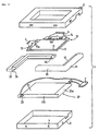
- liquid crystal display 1 The basic structure of one embodiment of liquid crystal display 1 will be explained using the cross-sectional view of liquid crystal display 1 shown in FIG. 2 and the break-down view of liquid crystal display 1 shown in FIG. 3.
- illumination device 20 is installed in lower case 3.
- liquid crystal display panel 10 is installed using frame 30 and 31.
- Liquid crystal display panel 10 is formed by enclosing the liquid crystal, transparent electrodes and such between two layers of transparent glass substrates 11 and 12.
- a plurality of driver ICs 13 are installed for latching pixel data for the rows and sending it to the liquid crystal display panel.
- driver ICs 14 are installed for latching pixel data for the columns and sending it to the liquid crystal display panel.
- Frames 30 and 31 are used to protect illumination device 20 and to position it within the case. At the same time, it also fills the role of maintaining a fixed distance for gap 33 between illumination device 20 and liquid crystal display panel 10, for example, 0.2 - 1 mm. For this reason, frames 30 and 31 are prepared so that their lower halfs 34 and 35 support illumination device 20 and their upper halfs 36 and 37 act as spacers between illumination device 20 and liquid crystal display panel 10.
- the frame is divided into two pieces, however, the number of pieces is not . limited to two. For example, three pieces, four pieces, or even more is possible, and even just one piece is also conceivable.
- the frame need not cover the entire periphery of illumination device 20 or liquid crystal display panel 10. A plurality of pieces may be arranged in appropriate places.
- Illumination device 20 is a surface-type illumination device set up with a cylindrically-shaped fluorescent light 22 at the edge of substantially rectangular light guide plate 21.
- Fluorescent light 22 is roughly L-shaped and is covered by reflectors 23a and 23b.
- Wires for supplying power to drive fluorescent light 22 extend from both ends of fluorescent light 22 and are connected to the driver circuit on the host side through connector 7 which is for turning on the light.
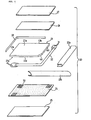
- FIG. 4 is a break-down view of illumination device 20 and will be used to explain the structure of this embodiment of the illumination device.
- Illumination device 20 is comprised of light guide plate 21, which is substantially rectangular in shape and is missing the comer of edge 40, fluorescent light 22, which encompasses edge 40 in an L-shape, and reflectors 23a and 23b, which cover fluorescent light 22 in the direction of light guide plate 21 and efficiently reflect light from fluorescent light 22 to light guide plate 21.
- light guide plate 21 On lower surface 21b of light guide plate 21, the side opposite of the side where liquid crystal display panel 10 is arranged, pattern sheet 24, which is printed with diffusion pattern 50, and reflecting sheet 25 are arranged in that order.
- diffusion sheet 26 and prism sheet 27 are arranged on upper surface 21a of light guide plate 21, the side where liquid crystal display panel 10 is arranged.
- Edge reflective tape 28 is installed at edge 41a and 41b, opposite fluorescent light 22 of light guide plate 21.
- Light guide plate 21 is a transparent material whose index of refraction is greater than that of air.
- An index of refraction equal to or greater than 1.41 is desirable using such materials as acrylic resin, polycarbonate resin, amorphous polyolefine-type resin, and polystyrene resin. Use of these type of materials for light guide plate 21 result in a critical angle of 45° or less. If upper surface 21a and lower surface 21b are smooth and mirror-like, the light incident from edges 41a, 41b, 41c, and 41d, which are formed at right angles to surface 21a and 21b, is completely reflected from surfaces 21a and 21b.
- Pattern sheet 24 is a transparent sheet with a fixed number of diffusion patterns 50 printed on it, the printed diffusion patterns being adhered to the lower surface 21b of light guide plate 21. Light incident from sides 41, to some extent, reach diffusion pattern 50 and, without being completely reflected will be diffused in the direction of upper surface 21a. Consequently, light incident from the fluorescent light by way of edges is emitted to the liquid crystal display panel 10 from upper surface 21a.
- Reflecting sheet 25 is a thin PET sheet with a thickness approximately 0.05 - 0.5 mm. Light coming from upper surface 21a from light guide plate 21 through diffusion pattern 50 travels through the diffusion sheet 26 or prism sheet 27, which are arranged on the upper portion of upper surface 21a and light up liquid crystal display panel 10. However, a portion of the light is reflected through sheet 26 and 27 in the lower direction. The light reflected from the upper direction is returned to light guide plate 21, among others, through reflecting sheet 25. Reflecting sheet 25 may also be aluminum or other non-PET material. Also, lower case 3 may be used in place of a reflecting sheet as a reflector. Further, the frame of a computer or such carrying the illumination device or liquid crystal display of the instant invention can also be used as a reflector in place of the reflecting sheet.
- Diffusion sheet 26 is an approximately 0.05 0.5 mm thin PET sheet or PC sheet. Diffusion sheet 26 diffuses the light that is reflected by diffusion pattern 50 and radiated from upper surface 21a. Diffusion pattern 50 is often formed in a narrow line configuration or net configuration. The light that is reflected by these types of patterns is diffused by diffusion sheet 26. The diffusion pattern cannot be recognized from the liquid crystal display panel 10. Diffusion sheet 26 is arranged with a very small layer of air between it and the upper surface 21a of light guide plate 21. The angle mentioned above is maintained in regards to the angle of upper surface 21a. Reflection sheet 26 is not limited to a PET sheet and such sheets as acrylic-type sheets, among others, may be used.
- Prism sheet 27, which is arranged on diffusion sheet 26, is made up of very small linear prisms lined in a cross-sectional array.
- the angle of the light radiating from diffusion sheet 26 is arranged to improve the illuminating intensity of the liquid crystal display panel 10.
- the brightness can be improved through prism sheet 27, when sufficient brightness is achieved through diffusion sheet 26, prism sheet 27 can be omitted, thus reducing manufacturing cost.
- Fluorescent light 22, which is used as the light source of illumination device 20, is in an L-shape, and is positioned adjacent to edges 41c and 41d of light guide plate 21. It is desirable, as will be explained later, to maintain a gap between edges 41c and 41d and fluorescent light 22 of around 0.8 -1.5 mm.
- the corner of edge 40 of light guide plate 21 is removed and the fluorescent light 22 is able to be positioned with the above noted gap. Also, through removing this corner, fluorescent light 22 and the corner of light guide plate 21 are kept from touching and such things as damage to the fluorescent light can be prevented.
- Fluorescent light 22 is covered by reflectors 23a and 23b to make the light discharged from fluorescent light 22 incident with good efficiency from edge 40 of light guide plate 21.
- Reflectors 23a and 23b are PET sheets deposited with silver and of a thickness of approximately 0.01 - 0.1 mm. In order to provide low cost reflectors that cover the L-shaped fluorescent light and that are easy to install, two straight reflectors are used. This will be explained in greater detail below.
- Edge reflective tape 28 is arranged at the two edges 41a and 41b, which are opposite the edges 41c and 41d where fluorescent light 22 and reflector 23 are installed.
- Edge reflective tape 28 is a PET sheet deposited with silver with thickness of approximately 0.01 - 0.1 mm. The light introduced to light guide plate 21 from fluorescent light 22 is completely reflected away. The light that reaches the edges of the opposite side is returned back to light guide plate 21. Materials such as white PET sheets, aluminum, and such can be used for the edge reflective tape as well as the reflectors mentioned above. It is also possible to integrate these into the case or frame as well.
- FIG. 5 shows the instalment of liquid crystal display panel 10 on illumination device 20.
- Driver IC 13 and 14 are arranged on sides 10a and 10b, adjacent to liquid crystal display panel 10. Opposite sides 10a and 10b, L-shaped fluorescent light 22 extends along the two sides 20c and 20d of illumination device 20. Because of this arrangement, driver IC 13 and 14 are not directly influenced by the heat from fluorescent light 22. Consequently, the temperature of the driver IC does not rise significantly, preventing changes in the driver's threshold value. For this reason, an image with very low fluctuations in contrast can be obtained using liquid crystal display panel 10.
- the temperature distribution of the entire liquid crystal display panel 10 becomes flat.
- high brightness is essential.
- the output of conventional fluorescent lights that are installed at one edge is increased and the slope of the temperature distribution of the liquid crystal display panel becomes large. This results in color and brightness irregularities and poor display quality.
- a rise in the temperature of the liquid crystal display panel can be suppressed and high brightness obtained.
- the light conversion efficiency can be increased through using an L-shaped fluorescent light, temperature rise can be further prevented.
- the majority of the power input into the fluorescent light is consumed as a cathode drop voltage which generates glow discharge.
- the cathode drop voltage consumed by glow discharge does not increase that much. Because of this, when two times the power is supplied, most of the increased power is consumed as a positive column gradient voltage in generating light. Consequently, the same brightness can be obtained with lower voltage and lower temperature rise.
- the rise of the temperature of the liquid crystal display panel can be held down and a good quality image can be obtained. Also, because the power consumption can be kept down, it is a suitable illumination device to be used for illumination in liquid crystal display panels in small, portable devices where batteries are used as the power source.
- edge 40 which interferes with fluorescent light 22 is removed so that the comer does not stick out and gap 42 is reduced.
- damage to fluorescent light 22 due to comer 43 impacting fluorescent light 22 during shipping and such can be prevented.
- damage to fluorescent light 22 caused by thermal expansion of light guide plate 21, vibration, and such can be prevented.
- Gap 42 between edge 41 and fluorescent light 22 is not completely eliminated. Not only do problems with precision during product manufacturing exist, but if gap 42 is reduced too much, the light reflected to reflector 23 is absorbed by fluorescent light 22 and the introduction efficiency from surface 41 is reduced. In FIG. 7, the light radiated from fluorescent light 22 to the opposite side of edge 40 is reflected by reflector 23 and introduced to edge 40. Consequently, if gap 42 is too small, the reflected light is introduced to fluorescent light 22 and completely absorbed within fluorescent light 22 and, thus, the amount of light introduced to edge 40 is reduced. If gap 42 is large, the incident efficiency improves, but when the distance of gap 42 exceeds a prescribed value, the increase in the incident efficiency becomes less to the extent that limiting the size of illumination system 20 becomes more desirable. An appropriate gap 42 is judged by this inventor to be approximately 0.8 - 1.5 mm. More specifically, in the case of fluorescent light 22 with a diameter of 2.5 - 4 mm, a gap of around 1 - 1.5 mm is desirable.
- the light reflected from reflector 23 is an important light source for illumination device 20.
- one method as shown in FIG. 8, is to use two reflectors 23a and 23b which are made from flat material and bent in a nearly half circular shape.
- Reflector 23a corresponds to the short side of light guide plate 21 and is long enough to cover from bent portion 22a to electrode 22c of the short side of bent fluorescent light 22.
- reflector 22b corresponds to the long side of light guide plate 21 and is long enough to cover from bent portion 22a to electrode 22c on the long side of bent fluorescent light 22.
- one of the reflectors is first arranged, for example, the shorter reflector 23a. If the next reflector is laid from the top of the first reflector to the other side, for example, longer reflector 23b, fluorescent light 22 can be completely covered. In this way, two separate reflectors 23a and 23b can be used to easily cover bent fluorescent light 22 and assembly of the reflector is made easy. Also, in conforming to the bent-shape of fluorescent light 22, reflector 23a and 23b do not have a complex shape, but rather, a simple straight-line shape is used and therefore manufacturing cost can be kept down.
- the aperture ratio is vital to raising the incident efficiency from fluorescent light 22 to edge 40.
- a desirable range for this aperture ratio which is defined as [(thickness of light guide plate 21) / (diameter of fluorescent light 22)], is around 0.9 - 2. If the aperture ratio is higher, the incident efficiency does not improve much.
- edge 40 The removal of several different types of shapes from the corner of edge 40 is possible.
- a corner in the shape of an isosceles triangle is removed from edge 40.
- Edge 43 which makes an angle of approximately 45° with respect to both edge 41c and 41d, is formed by edge 40. Because the light directly incident to edges 41c and 41d from fluorescent light 22 is reflected at edge 40, the influence of this portion to the intensity of the light radiated from upper surface 21a of light guide plate 21 is small. The influence of this removed shape to the uniformity of the brightness is small. However, with the scattered light that differs from the incident angle, there is the fear that the brightness uniformity incident from edge 43 and radiated from upper surface 21 will be hindered.
- reflective member 44 is installed to prevent light incident to light guide plate 21 from edge 43.
- a plastic sheet deposited with white, silver, or aluminum among others or even a molded part can be used as reflecting member 44. This reflects light rays from leaving light guide plate 21 and passing through edge 43 and, oppositely, shields light rays entering from fluorescent light 22, maintaining brightness uniformity.
- edge 40 becomes larger, the light introduced from light guide plate 21 is reduced in the vicinity of the edge. Consequently, in order to maintain uniformity of brightness, it is desirable to establish limitations for the size of the triangle shape that will be removed. On one hand, if too little is removed, gap 42 between fluorescent light 22 and edge 41 cannot be properly maintained. Considering this, it is found desirable to make the length of the substantially equal in length sides of the triangle to be, within the range of 0.6 to 1.0 times the smallest radius of curvature of bent portion 22a of fluorescent light 22.
- FIG. 10 shows other shape possibilities that are used in other embodiments of the invention.
- FIGS. 10(a) and 10(b) are examples of the corner removed from edge 40 being parallel to adjacent sides 41c and 41d.
- edge 40 should be cut in a diamond shape, or in a square shape if the light guide plate is rectangular.
- Edges 45a and 45b, which are cut in a diamond-shape, are approximately parallel to adjacent edges 41c and 41d of light guide plate 21. Consequently, the light introduced to light guide plate 21 from these edges 45a and 45b have substantially the same vector as edges 41c and 41d, and the probability of light being incident from the edges or being emitted is substantially the same.
- edge 40 it is rare for edge 40 to exert an influence on the uniformity of the brightness of the light radiated from the illumination device. For this reason, even if reflecting member 44 is omitted, it is still possible to obtain uniform brightness. However, it is difficult to maintain good uniformity if the gap between the edge and the fluorescent light becomes large. In considering the fluorescent light and interference, it is found to be desirable to make the length of one of the diamond-shaped sides, as noted above, to be within the range of 0.6 to 1.0 times the smallest radius of curvature of bent portion 22a of fluorescent light 22.
- FIGS. 10(c) and 10(d) show examples of shapes of edge 40 when attention is paid to the manufacturing process of light guide plate 21.
- a "fan-shape" as shown in FIG. 10(c) can be used.
- an "opposite fan-shape” is also possible.
- other shapes are also possible.
- FIG. 11 shows diffusion pattern 50 for emitting light introduced to light guide plate 21 from bent fluorescent light 22 to the liquid crystal display panel from upper surface 21a of light guide plate 21.
- diffusion pattern 50 is printed on pattern sheet 42, it is also possible to print directly on lower surface 21b of light guide plate 21. It also is, of course, possible to draw diffusion pattern 50 on the lower surface of light guide plate 21 through such methods as etching.
- line patterns and dot patterns are most commonly used, other patterns, as well as increasing or decreasing the pattern area density at different places is also possible.
- FIG. 11 shows an example of a pattern where the area of the dots are increased or decreased.
- the dot areas are small near edges 41c and 41d where fluorescent light 22 is positioned and these areas gradually increase as they move towards the opposing edges 41a and 41b.
- the area near edge 40 which is by bent portion 22a of.fluorescent light 22 has the smallest areas and the comer opposite this between edge 41a and 41b has the largest areas.
- the density distribution S(x,y) of this diffusion pattern in accordance with the invention is described below.
- x and y are coordinates along edges 41c and 41d of fluorescent light 22, and a coordinate axis is used that increases in the direction away from fluorescent light 22.
- the density distribution of a diffusion pattern is assumed in advance to be Sx i y j .
- the intensity of the light diffused at each small area using the compensated density distribution S 1 x i y j of the diffusion pattern is recalculated. If this intensity can be kept within the permitted range, a diffusion pattern with proper brightness uniformity will be generated. If, despite using the once compensated density distribution S 1 x i y j , the intensity of the light is not kept within the fixed range, repeat the compensation with the above technique.
- the intensity of the light emitted by diffusion at each co-ordinate, or each small area is calculated for all directions.
- the average light intensity is found and the density distribution of the diffusion pattern is compensated so that variations of the light intensity emitted from each small area will be kept within the average light intensity and fixed range.
- edge reflective tape 28 which is placed on edges 41a and 41b.
- edge reflective tape 28 For the intensity of the light reflected from edge 41a and 41b by edge reflective tape, it is appropriate to add the intensity of the light that is diffused and emitted to the calculation of l i,j , the intensity of light emitted from each small area.
- Lx the intensity of light reflected from edge 41a in the x direction.
- ⁇ is the reflection coefficient of the edge reflective tape.
- a number, for example, such as 0.5 may be used. Consequently, by performing a further calculation to that discussed above, a density distribution of the diffusion pattern compensated for edge reflection can be generated for the light source of the intensity incident from co-ordinate x a in the x direction. And, by using diffusion pattern 50 which follows this density distribution, illumination with a high uniform brightness can be achieved through the light guide plate.
- FIG. 12 shows an example in accordance with the invention of increasing and decreasing the thickness of the light guide plate instead of forming a diffusion pattern that differs in density on the light guide plate.
- diffusion pattern 51 which has a fixed density distribution
- the cross section of light guide plate 29 is formed in inversely proportional to the density distribution of the diffusion pattern discussed above.
- edges 41c and 41d of light guide plate 29 are thick and the thickness become gradually thinner in the direction of edges 41a and 41b.
- a light guide plate such as light guide plate 29 shown in FIG. 12 can, therefore, also obtain illumination with high uniform brightness.
- the density distribution of the diffusion pattern and the thickness distribution of the light guide plate may be used in combination to provide illumination with high uniform brightness.
- Illumination device 10 uses as its light source one long fluorescent light that is bent in an L-shape and can be installed at the light guide plate which has a comer removed. Consequently, the effective overall length of the fluorescent light can be extended and the gross luminous energy raised without increasing the number of driver circuits used for turning on the fluorescent light. Also, the necessity when there are a plurality of fluorescent lights to adjust such things as the driver circuit so the brightness of the plurality of fluorescent lights are in agreement does not exist. Further, because the light conversion efficiency can be raised, power consumption can be reduced. In terms of the output of the driver circuit for turning on the fluorescent light, although it is necessary to raise the output ability because the overall length of the fluorescent light is extended, when compared with the case of turning on two fluorescent lights, the output of the driver circuit is low.
- Illumination device 10 has various uses as a surface-type illuminant besides the liquid crystal display discussed above.
- the fluorescent light can be arranged in a place opposite the liquid crystal driver IC because an L-shape fluorescent light is used. For this reason, the effects of heat from the illuminant to the driver IC can be kept to a minimum and a stable display obtained.
- the illuminant and driver IC have no positional interferences, the size of the liquid crystal display can be reduced.
- the power consumption of the illumination system is low, the heating power per unit length is low as the illuminating portion is long, and the temperature rise of the liquid crystal panel can, to a great extent, be kept down. Consequently, when high brightness necessary for color displays is shown, color and brightness irregularities of the liquid crystal panel can be prevented and a good quality, vivid color display obtained.
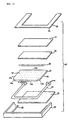
- FIG. 13 shows a liquid crystal display using an illumination device 60, which differs from that described above, and liquid crystal panel 10 installed on illumination system 60. Concerning this liquid crystal display, the drawings and descriptions substantially similar to the embodiment shown in FIG. 1 are eliminated. Also, the same figure numbers for liquid crystal display panel 10 and other parts that are in common with the first embodiment will be used and the descriptions eliminated.
- Illumination device 60 uses a U-shaped fluorescent light 62 as a light source. Fluorescent light 62 is positioned next to edges 41a, 41c and 41d, three of the four edges 41a - 41d formed on light guide plate 61 of illumination system 60. Illumination device 60 is enclosed within frames 38 and 39, which are divided into an upper and lower section. Upper frame 38 acts as a spacer to secure the gap between liquid crystal display panel 10 and illumination device 60.
- illumination device 60 of this embodiment will be explained using FIGS. 14 and 15.
- U-shaped fluorescent light 62 is installed next to three of the edges of light guide plate 61, 41a, 41c, and 41d.
- the remaining edge 41b is equipped with edge reflecting tape 28.
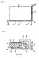
- the mirror surface of the hyperbolic curve section of the inner surface 63 of lower frame 39 is formed by silver deposition or the like.
- the lower surface 64 of upper frame 38 is also silver deposited and mirrorized.
- the inner surface 63 and lower surface 64 of frame 39 and 38, respectively, perform the function of a reflector, thus integrating the reflector and frame described in the previous embodiment into one part. Consequently, the troubles due to assembling illumination device 60 is further reduced.
- reflection sheet 25, diffusion sheet 26, and prism 27 will be omitted as they are the same as that explained in the earlier embodiment.
- the pattern sheet is omitted because the diffusion sheet 52 is printed on lower surface 61b of light guide plate 61.
- the two corners are removed from edge 40a and 40b of light guide plate 61 in order to install U-shaped fluorescent light 62 with an appropriate gap 42 at the light guide plate, as has explained in the embodiment above.
- FIG. 16 shows the relationship of fluorescent light 62 and light guide plate 61.
- the corners of edge 40b, which is between edges 41c and 41d, and edge 40a, which is between edges 41a and 41d, are removed so that they do not stick out.
- fluorescent light 62 can be installed with fixed gap 42 near edge 41, and the incident efficiency towards light guide plate 61 maintained at a high level. Also, damage to fluorescent light 62 due to such things as thermal expansion and shock can be prevented.
- the shape of the removed corner in this example, is a triangle with two sides of approximate equal length. However, as explained earlier, it is of course possible to use other shapes as well.
- FIG. 17 shows diffusion pattern 52, which is printed on light guide plate 61, when looking from the direction of lower side 21b of light guide plate 21.
- Diffusion pattern 52 is formed by using the density distribution generated by the generation method discussed above in accordance with the invention.
- edge 41c there is a light source 41a
- the area density of the diffusion pattern on this side is low and the area density of the diffusion pattern in the middle of lower surface 21b is high.
- the area density of the diffusion pattern along edge 41d is low, and the area density of the diffusion pattern opposite this side near edge 41b is high.
- the light introduced to light guide plate 61 is diffused and a uniform light is released from upper surface 61a of light guide plate 61 towards the liquid crystal display panel.
- FIG. 18 shows the temperature distribution on liquid crystal display panel 10 of this embodiment of the invention. From viewing this graph it can be seen that the temperature rise of the panel directly on the fluorescent light only increases about 10 degrees above the regular temperature. As shown from FIG. 22, this a great reduction from when a conventional illumination device is used. Because of very little difference between the temperature of the central portion of the liquid crystal display panel and the temperature of the edge portion near the light source and the resulting flat temperature distribution, there is a very low amount of image and brightness irregularities that appear on the liquid crystal display panel. Consequently, a good quality image can be obtained. Therefore, illumination device 50 is an illumination device that can irradiate a light of high brightness for color displays and can prevent a temperature rise on the liquid crystal display panel. Because of the use of a long light source bent in a U-shape, the amount of heating per unit length can be reduced and, still further, a reduction in power consumption achieved.
- driver IC 13 is arranged on one of the sides of the U-shaped fluorescent light.
- thermal expansion towards driver IC is low and problems such as fluctuations in the threshold value can be controlled. Consequently, the liquid crystal display of this embodiment can obtain a vivid and stable color image with high brightness and low power consumption.
- devices that use liquid crystal displays, such as televisions and personal computers can be miniaturized. Because the discharge length is increased, the driver circuit output must be improved to turn on the U-shaped fluorescent light. However, when compared to turning on three separate fluorescent lights, the increase in output of the driver circuit is small.
- FIG. 19 shows an example of two approximately L-shaped fluorescent lights 72a and 72b installed on light guide plate 71.
- FIG. 20 shows three approximately L-shaped fluorescent lights 82a, 82b, and 82c installed on hexagonal light guide plate 81. The corners are removed from the edge portion 40 of both light guide plate 71 and 81 so that there is no interference with fluorescent light 72 and 82 and so that these lights can be properly positioned. Structures discussed in the above embodiments, such as those of the reflectors, can be used.
- Various shapes of surface-type illumination systems can be formed using a bent, cylindrical illuminant. With these illumination devices, a uniform illumination device with high brightness can be obtained that has low.power consumption. Also, a high quality color display can be obtained when using a color liquid crystal display panel.
- This surface-type illumination device is suitable for use as a backlight in liquid crystal display devices that use a liquid crystal display panel or for use as other flat, surface-type illumination devices. Because liquid crystal display devices using this illumination device can display vivid color with low power consumption, it can be used as a display in notebook PCs and other information processing devices as well as in devices such as liquid crystal TVs, video cameras, and other image processing devices.
Landscapes
- Physics & Mathematics (AREA)
- General Physics & Mathematics (AREA)
- Optics & Photonics (AREA)
- Nonlinear Science (AREA)
- Crystallography & Structural Chemistry (AREA)
- Mathematical Physics (AREA)
- Chemical & Material Sciences (AREA)
- Engineering & Computer Science (AREA)
- General Engineering & Computer Science (AREA)
- Manufacturing & Machinery (AREA)
- Liquid Crystal (AREA)
- Planar Illumination Modules (AREA)
- Light Guides In General And Applications Therefor (AREA)
- Devices For Indicating Variable Information By Combining Individual Elements (AREA)
- Vessels And Coating Films For Discharge Lamps (AREA)
Claims (6)
- Dispositif d'éclairage, comprenant :en ce que la répartition d'intensité pour une deuxième direction sensiblement parallèle audit deuxième bord latéral (41d) et basée sur l'intensité de la lumière incidente provenant dudit élément illuminant allongé (22) sur ledit premier bord latéral (41c), à des coordonnées rectangulaires arbitraires à n'importe quel point du côté avant émettant de la lumière de ladite plaque de guidage de lumière (21), fournisse une répartition lumineuse sensiblement uniforme au niveau de l'ensemble des coordonnées rectangulaires arbitraires du côté avant émettant de la lumière.une plaque de guidage de lumière (21) possédant un côté avant émettant de la lumière et qui est de forme polygonale et sensiblement transparente ;un moyen de source d'éclairage comprenant un élément illuminant allongé (22) formé afin d'intégrer une section en forme de L ou en forme de U afin de faire face au moins à un premier et un deuxième bords latéraux contigus (41c, 41d) de ladite plaque de guidage de lumière ; etun motif de diffusion (50, 52) placé à l'arrière de ladite plaque de guidage de lumière, caractérisé en ce que la plaque de guidage de lumière possède une répartition d'épaisseur et/ou en ce que le motif de diffusion possède une répartition de densité qui est/sont agencée(s) de telle sorte que la somme de la répartition de l'intensité lumineuse dans une première direction sensiblement parallèle audit premier bord latéral (41c) et basée sur l'intensité de la lumière incidente provenant dudit élément illuminant allongé (22) sur ledit deuxième bord latéral (41 d), et
- Dispositif selon la revendication 1, comprenant un réflecteur de bord (28) sur au moins l'un des deux bords latéraux opposés au premier bord latéral (41c) et au deuxième bord latéral (41d), ledit réflecteur de bord reflétant la lumière provenant de la partie intérieure de ladite plaque de guidage de lumière jusqu'à ladite plaque de guidage de lumière (21), caractérisé en ce que l'épaisseur de la plaque de guidage de lumière et/ou la répartition de densité du motif de diffusion est/sont telle(s) que la somme de la répartition d'intensité lumineuse au niveau des coordonnées rectangulaires arbitraires, comprenant la répartition d'intensité de la lumière réflechie par au moins ledit réflecteur de bord (28) jusqu'à ladite plaque de guidage de lumière (21), fournisse ladite répartition lumineuse sensiblement uniforme au niveau de l'ensemble desdites coordonnées rectangulaires arbitraires du côté avant émettant de la lumière.
- Dispositif selon la revendication 1 ou 2, comprenant en outre un affichage à cristaux liquides (10) qui est éclairé par la lumière émise par le côté avant émettant de la lumière de ladite plaque de guidage de lumière par un motif de diffusion (50) formé sur le côté arrière de ladite plaque de guidage de lumière, et
un circuit d'entraínement (13, 14) qui alimente ledit affichage à cristaux liquides, ledit circuit d'entraínement étant agencé le long d'un bord latéral de ladite plaque de guidage de lumière. - Procédé d'établissement d'une densité de diffusion d'un motif de diffusion, et/ou d'une répartition d'épaisseur d'une plaque de guidage de lumière transparente et de forme polygonale (21) dans un dispositif d'éclairage de surface comprenant un élément illuminant allongé (22) formé afin d'intégrer une section en forme de L ou en forme de U faisant face à au moins un premier bord latéral et un deuxième bord latéral contigu (41c, d) de la dite plaque de guidage de lumière, et un motif de diffusion (50, 52) disposé sur un côté arrière de ladite plaque de guidage de lumière afin de garantir que la lumière est répartie de manière uniforme sur un côté avant émettant de la lumière de ladite plaque de guidage de lumière, le procédé étant caractérisé par :la détermination d'une première répartition d'intensité de lumière émise pour une première direction sensiblement parallèle audit premier bord latéral (41c) basée sur l'intensité de la lumière incidente allant jusqu'à ladite plaque de guidage de lumière (21) depuis ledit deuxième bord latéral (41d) et un premier motif de diffusion possédant une première répartition de densité et/ou une première répartition d'épaisseur de ladite plaque de guidage de lumière (21) ;la détermination d'une deuxième répartition d'intensité de lumière émise pour une deuxième direction le long dudit deuxième bord latéral (41d) basée sur l'intensité de la lumière incidente allant jusqu'à ladite plaque de guidage de lumière (21) depuis ledit premier bord latéral (41c) et le premier motif de diffusion possédant la première répartition de densité et/ou ladite première répartition d'épaisseur de ladite plaque de guidage de lumière (21) ; etle calcul d'une répartition de densité compensée dudit motif de diffusion et/ou d'une répartition d'épaisseur révisée de ladite plaque de guidage de lumière (21) en compensant la répartition de densité dudit premier motif de diffusion et/ou ladite première répartition d'épaisseur de ladite plaque de guidage de lumière (21) de telle sorte que la somme de ladite première répartition d'intensité de lumière émise et de ladite deuxième répartition d'intensité de lumière émise fournisse une répartition lumineuse sensiblement uniforme au niveau de l'ensemble des coordonnées rectangulaires arbitraires du côté avant émettant de la lumière de ladite plaque de guidage de lumière.
- Procédé de motif de diffusion selon la revendication 5, le dispositif comprenant un réflecteur de bord (28) situé au moins sur l'un des deux côtés latéraux opposés au premier côté latéral (41c) et au deuxième côté latéral (41d), ledit réflecteur de bord (28) reflétant la lumière provenant de la partie intérieure de ladite plaque de guidage de lumière vers ladite plaque de guidage de lumière (21), le procédé étant en outre caractérisé par :le calcul de l'intensité de la lumière incidente réfléchie par ledit réflecteur de bord (28) jusqu'à ladite plaque de guidage de lumière (21) avec un facteur d'atténuation fixe ; etl'ajout d'une répartition d'intensité de lumière émise prédite pour au moins l'une d'une première et d'une deuxième directions découverte pour ladite intensité de lumière réflechie à la somme de la première répartition d'intensité de lumière émise et de ladite deuxième répartition d'intensité de lumière émise, qui se trouvent sur les coordonnées rectangulaires arbitraires de ladite plaque de guidage de lumière (21).
- Procédé selon la revendication 4 ou 5, caractérisé en ce que l'étape de compensation est représentée comme suit :
Applications Claiming Priority (7)
| Application Number | Priority Date | Filing Date | Title |
|---|---|---|---|
| JP18497692 | 1992-07-13 | ||
| JP18497692 | 1992-07-13 | ||
| JP184976/92 | 1992-07-13 | ||
| JP11185293 | 1993-05-13 | ||
| JP11185293 | 1993-05-13 | ||
| JP111852/93 | 1993-05-13 | ||
| EP93914993A EP0607453B1 (fr) | 1992-07-13 | 1993-07-13 | Dispositif d'eclairage de surface et affichage a cristaux liquides |
Related Parent Applications (2)
| Application Number | Title | Priority Date | Filing Date |
|---|---|---|---|
| EP93914993A Division EP0607453B1 (fr) | 1992-07-13 | 1993-07-13 | Dispositif d'eclairage de surface et affichage a cristaux liquides |
| EP93914993.6 Division | 1994-01-20 |
Publications (2)
| Publication Number | Publication Date |
|---|---|
| EP0798507A1 EP0798507A1 (fr) | 1997-10-01 |
| EP0798507B1 true EP0798507B1 (fr) | 2004-03-03 |
Family
ID=26451157
Family Applications (2)
| Application Number | Title | Priority Date | Filing Date |
|---|---|---|---|
| EP97201696A Expired - Lifetime EP0798507B1 (fr) | 1992-07-13 | 1993-07-13 | Dispositif d'éclairage de surface et affichage à cristaux liquides |
| EP93914993A Expired - Lifetime EP0607453B1 (fr) | 1992-07-13 | 1993-07-13 | Dispositif d'eclairage de surface et affichage a cristaux liquides |
Family Applications After (1)
| Application Number | Title | Priority Date | Filing Date |
|---|---|---|---|
| EP93914993A Expired - Lifetime EP0607453B1 (fr) | 1992-07-13 | 1993-07-13 | Dispositif d'eclairage de surface et affichage a cristaux liquides |
Country Status (5)
| Country | Link |
|---|---|
| US (3) | US5619351A (fr) |
| EP (2) | EP0798507B1 (fr) |
| JP (5) | JP3256970B2 (fr) |
| DE (2) | DE69331896T2 (fr) |
| WO (1) | WO1994001795A1 (fr) |
Families Citing this family (133)
| Publication number | Priority date | Publication date | Assignee | Title |
|---|---|---|---|---|
| EP0798507B1 (fr) * | 1992-07-13 | 2004-03-03 | Seiko Epson Corporation | Dispositif d'éclairage de surface et affichage à cristaux liquides |
| US5640216A (en) * | 1994-04-13 | 1997-06-17 | Hitachi, Ltd. | Liquid crystal display device having video signal driving circuit mounted on one side and housing |
| JP3434053B2 (ja) * | 1994-11-30 | 2003-08-04 | ハリソン東芝ライティング株式会社 | バックライトおよびこれを用いた液晶表示装置 |
| EP0717236B1 (fr) * | 1994-12-16 | 2001-08-16 | Canon Kabushiki Kaisha | Dispositif d'illumination et afficheur à cristaux liquides le comprenant |
| US5796450A (en) * | 1994-12-16 | 1998-08-18 | Canon Kabushiki Kaisha | Illumination device and liquid crystal display apparatus including same |
| US7108414B2 (en) | 1995-06-27 | 2006-09-19 | Solid State Opto Limited | Light emitting panel assemblies |
| JP3790571B2 (ja) * | 1995-11-06 | 2006-06-28 | 株式会社きもと | 光拡散性シートおよびそれを用いた液晶ディスプレイ用バックライトユニット |
| JPH09147618A (ja) * | 1995-11-20 | 1997-06-06 | Sharp Corp | 照明装置 |
| US6219117B1 (en) * | 1996-06-12 | 2001-04-17 | Alps Electric Co., Ltd. | Liquid crystal display device |
| TW464784B (en) * | 1996-12-06 | 2001-11-21 | Alps Electric Co Ltd | Liquid crystal display device |
| DE19652209A1 (de) * | 1996-12-16 | 1998-06-18 | Bosch Gmbh Robert | Beleuchtungseinheit |
| DE19700472A1 (de) * | 1997-01-09 | 1998-07-23 | Bosch Gmbh Robert | Beleuchtungseinheit |
| KR100229615B1 (ko) * | 1997-01-28 | 1999-11-15 | 구자홍 | 액정표시장치 |
| US5896229A (en) * | 1997-02-20 | 1999-04-20 | Ericsson Inc. | Discretely applied diffusor structures on lightguides |
| US6838810B1 (en) * | 1997-03-21 | 2005-01-04 | Chunghwa Picture Tubes, Ltd. | Flat-panel display mounting system for portable computer |
| HU224147B1 (hu) * | 1997-03-21 | 2005-05-30 | Patent-Treuhand-Gesellschaft für elektrische Glühlampen mbH. | Lapos fénycső háttérvilágításhoz, valamint ilyen fénycsövet tartalmazó világítási rendszer és LCD kijelzős készülék |
| KR100218581B1 (ko) * | 1997-04-08 | 1999-09-01 | 구자홍 | 액정표시장치를 가지는 휴대용 컴퓨터 |
| US7492421B1 (en) | 1997-07-03 | 2009-02-17 | Lg Display Co., Ltd. | Case for liquid crystal display |
| JP3654410B2 (ja) * | 1997-08-11 | 2005-06-02 | 株式会社エンプラス | サイドライト型面光源装置、液晶表示装置及び導光板 |
| JP4042829B2 (ja) * | 1998-04-01 | 2008-02-06 | 矢崎総業株式会社 | 液晶表示装置 |
| GB2340280A (en) * | 1998-08-03 | 2000-02-16 | Lite On Electronics Inc | Grating structure for lightguide of a display backlight |
| JP3666265B2 (ja) | 1998-08-20 | 2005-06-29 | 松下電器産業株式会社 | 照明ユニットとそれを用いた液晶表示装置 |
| DE19844889A1 (de) | 1998-09-30 | 2000-04-06 | Patent Treuhand Ges Fuer Elektrische Gluehlampen Mbh | Dimmbare Beleuchtungsvorrichtung |
| US6501641B1 (en) * | 1998-10-23 | 2002-12-31 | Lg. Philips Lcd Co. Ltd. | Portable computer having a flat panel display device |
| KR100508003B1 (ko) * | 1998-11-11 | 2005-11-21 | 엘지.필립스 엘시디 주식회사 | 휴대용컴퓨터와그평판표시장치의결합방법 |
| JP3331326B2 (ja) * | 1998-11-13 | 2002-10-07 | 株式会社東芝 | 面光源装置及びこれを用いた平面表示装置 |
| DE19858810A1 (de) | 1998-12-21 | 2000-06-29 | Patent Treuhand Ges Fuer Elektrische Gluehlampen Mbh | Flache Beleuchtungsvorrichtung und Betriebsverfahren |
| JP2002533892A (ja) | 1998-12-29 | 2002-10-08 | オスラム オプト セミコンダクターズ ゲゼルシャフト ミット ベシュレンクテル ハフツング | 側方に斜めの光入力結合部を有する光源素子 |
| USD438331S1 (en) | 1999-03-19 | 2001-02-27 | Moriyama Sangyo Kabushiki Kaisha | Translucent color filter |
| JP3565101B2 (ja) * | 1999-08-11 | 2004-09-15 | セイコーエプソン株式会社 | サイドライト型面光源装置およびその製造方法、電気光学装置ならびに電子機器 |
| JP2001117516A (ja) | 1999-10-15 | 2001-04-27 | Ichiyosha:Kk | 面発光ディスプレーパネル |
| JP2001166150A (ja) * | 1999-12-13 | 2001-06-22 | Nitto Denko Corp | 導光板、面光源装置及び液晶表示装置 |
| JP4387532B2 (ja) * | 1999-12-24 | 2009-12-16 | 東芝モバイルディスプレイ株式会社 | 平面表示装置のバックライトユニット |
| JP3719927B2 (ja) * | 1999-12-27 | 2005-11-24 | シャープ株式会社 | 照明装置及び液晶表示器 |
| US6390638B1 (en) * | 2000-02-10 | 2002-05-21 | Ide, Inc. | Bulb wrap using expanded polytetrafluoroethylene |
| EP1136752A1 (fr) * | 2000-03-24 | 2001-09-26 | Nec Corporation | Unité pour rétroéclairage et dispositif d'affichage avec même unité pour rétroéclairage |
| US6674250B2 (en) | 2000-04-15 | 2004-01-06 | Guang-Sup Cho | Backlight including external electrode fluorescent lamp and method for driving the same |
| CA2310792A1 (fr) * | 2000-06-07 | 2001-12-07 | Stuart Engel | Lampe a rayonnement ultra-violet et reflecteur/ecran |
| KR100666321B1 (ko) * | 2000-06-30 | 2007-01-09 | 삼성전자주식회사 | 적층형 백라이트 어셈블리, 이를 적용한 액정표시장치 및이들의 조립 방법 |
| WO2002011406A2 (fr) | 2000-07-31 | 2002-02-07 | Koninklijke Philips Electronics N.V. | Dispositif d'affichage detecteur d'image |
| KR100701014B1 (ko) * | 2000-11-22 | 2007-03-29 | 삼성전자주식회사 | 광 가이드 장치, 이를 갖는 액정 표시 모듈 및 액정 표시장치 |
| JP2002196263A (ja) * | 2000-12-26 | 2002-07-12 | Ngk Insulators Ltd | ディスプレイ装置 |
| JP3690298B2 (ja) * | 2001-02-23 | 2005-08-31 | ソニーケミカル株式会社 | 液晶表示素子 |
| US8684584B2 (en) * | 2001-05-16 | 2014-04-01 | Benzion Inditsky | Ultra-thin backlight |
| US7001058B2 (en) * | 2001-05-16 | 2006-02-21 | Ben-Zion Inditsky | Ultra-thin backlight |
| KR100805127B1 (ko) * | 2001-05-17 | 2008-02-21 | 삼성전자주식회사 | 램프 와이어 고정홈을 갖는 액정표시장치 |
| KR20030008790A (ko) * | 2001-07-20 | 2003-01-29 | 삼성전자 주식회사 | 액정표시장치 |
| DE10137042A1 (de) * | 2001-07-31 | 2003-02-20 | Patent Treuhand Ges Fuer Elektrische Gluehlampen Mbh | Planare Lichtquelle auf LED-Basis |
| JP2003068115A (ja) * | 2001-08-30 | 2003-03-07 | Koito Mfg Co Ltd | 車両用灯具 |
| KR20030039602A (ko) * | 2001-11-13 | 2003-05-22 | 삼성전자주식회사 | 액정표시장치 |
| JP4045097B2 (ja) * | 2001-12-28 | 2008-02-13 | シャープ株式会社 | バックライト装置及びこれを用いた液晶表示装置 |
| KR100783592B1 (ko) * | 2002-02-05 | 2007-12-07 | 삼성전자주식회사 | 조명장치 및 이를 백라이트로 채택한 표시장치 |
| JP3773865B2 (ja) * | 2002-03-06 | 2006-05-10 | 三洋電機株式会社 | 導光板および表示装置 |
| JP3953857B2 (ja) | 2002-03-25 | 2007-08-08 | 株式会社アドバンスト・ディスプレイ | 面状光源装置及び面状光源装置の製造方法 |
| KR100840726B1 (ko) * | 2002-05-29 | 2008-06-23 | 삼성전자주식회사 | 백 라이트 어셈블리 및 이를 갖는 액정 표시 장치 |
| KR100840718B1 (ko) * | 2002-05-31 | 2008-06-23 | 삼성전자주식회사 | 백 라이트 어셈블리 및 이를 갖는 액정 표시 장치 |
| KR20040012393A (ko) * | 2002-08-03 | 2004-02-11 | 삼성전자주식회사 | 백라이트 어셈블리 및 이를 갖는 액정 표시 장치 |
| TWI232281B (en) * | 2002-08-16 | 2005-05-11 | Toppoly Optoelectronics Corp | A backlight device of a LCD display |
| AU2002330310A1 (en) * | 2002-09-19 | 2004-04-08 | Matsushita Electric Industrial Co., Ltd. | Illumination unit and liquid crystal display comprising it |
| TWI273291B (en) * | 2002-12-17 | 2007-02-11 | Hon Hai Prec Ind Co Ltd | Surface light source and light guide plate used therein |
| ES1053825Y (es) * | 2003-01-22 | 2003-09-01 | Guerra Navas Titular Al 50 Ant | Estructura para juego de sobremesa. |
| JP4179982B2 (ja) * | 2003-01-24 | 2008-11-12 | シャープ株式会社 | 面状照明装置およびそれを使用した液晶表示装置 |
| JP4255302B2 (ja) * | 2003-03-31 | 2009-04-15 | シャープ株式会社 | 液晶表示用照明装置および液晶表示装置 |
| US6820993B1 (en) * | 2003-08-20 | 2004-11-23 | Toppoly Optoelectronics Corp. | Planar light emitting mechanism |
| KR100567250B1 (ko) * | 2003-09-06 | 2006-04-03 | 현대모비스 주식회사 | 차량용 오디오의 액정표시모듈 |
| US20050057913A1 (en) * | 2003-09-16 | 2005-03-17 | Dennis Brett M. | Backlight having multiple intensity maxima |
| US20050094075A1 (en) * | 2003-10-29 | 2005-05-05 | Au Optronics Corporation | Multi-domain vertical alignment thin film transistor liquid crystal dispaly, color filter substrate and polarizer film applied thereto, and fabricating method thereof |
| GB0329205D0 (en) * | 2003-12-17 | 2004-01-21 | Graham Morton | An illumination device |
| TWI225560B (en) * | 2003-12-29 | 2004-12-21 | Au Optronics Corp | Edge light type backlight module and liquid crystal display |
| WO2005096045A2 (fr) * | 2004-03-23 | 2005-10-13 | E.I. Dupont De Nemours And Company | Guide lumineux et appareil utilisant ledit guide lumineux |
| KR100646137B1 (ko) | 2004-03-24 | 2006-11-15 | 토파즈엘시디 주식회사 | 백라이트 유닛용 도광판 |
| US7226195B2 (en) * | 2004-07-23 | 2007-06-05 | Thomas & Betts International | Cold-cathode fluorescent lamp assembly for lighting applications |
| CN100412648C (zh) * | 2004-08-06 | 2008-08-20 | 友达光电股份有限公司 | 背光组件 |
| JP4380494B2 (ja) | 2004-10-07 | 2009-12-09 | ソニー株式会社 | コンテンツ・マネジメント・システム及びコンテンツ・マネジメント方法、並びにコンピュータ・プログラム |
| CN100371791C (zh) * | 2004-11-09 | 2008-02-27 | 鸿富锦精密工业(深圳)有限公司 | 背光系统 |
| US20060114366A1 (en) * | 2004-12-01 | 2006-06-01 | Au Optronics Corporation | Flat-panel display apparatus |
| US20060120101A1 (en) * | 2004-12-02 | 2006-06-08 | Peng Juen T | Back light source for liquid crystal display |
| KR101035918B1 (ko) * | 2004-12-08 | 2011-05-23 | 엘지디스플레이 주식회사 | 직하형 백라이트 |
| TWM270373U (en) * | 2004-12-24 | 2005-07-11 | Innolux Display Corp | Light guide plate and backlight module |
| CN2769943Y (zh) * | 2004-12-30 | 2006-04-05 | 群康科技(深圳)有限公司 | 双面液晶显示装置 |
| WO2006098139A1 (fr) * | 2005-03-14 | 2006-09-21 | Tokuju Kogyo Co., Ltd | Dispositif d’eclairage et dispositif de culture de plantes equipe d’un dispositif d’eclairage |
| TWI264594B (en) * | 2005-04-01 | 2006-10-21 | Lite On Technology Corp | Back light module |
| CN2791690Y (zh) * | 2005-04-09 | 2006-06-28 | 群康科技(深圳)有限公司 | 导光板和背光模组 |
| KR101172253B1 (ko) * | 2005-05-10 | 2012-08-08 | 엘지디스플레이 주식회사 | 액정표시장치용 백라이트 유닛 |
| TWM278908U (en) * | 2005-05-23 | 2005-10-21 | Innolux Display Corp | Light guide plate and backlight module using the same |
| CN100403113C (zh) * | 2005-05-24 | 2008-07-16 | 群康科技(深圳)有限公司 | 背光模组及液晶显示装置 |
| JP2006330536A (ja) * | 2005-05-30 | 2006-12-07 | Sanyo Epson Imaging Devices Corp | 液晶表示装置 |
| EP1897146A2 (fr) * | 2005-06-27 | 2008-03-12 | Lamina Lighting, Inc. | Ensemble diode electroluminescente et procede de fabrication |
| JP4372117B2 (ja) * | 2005-06-30 | 2009-11-25 | 富士通テン株式会社 | 受信装置 |
| KR100651417B1 (ko) * | 2005-07-15 | 2006-11-29 | 삼성전자주식회사 | 휴대용 단말기의 키패드 조명 장치 |
| TWI287153B (en) * | 2005-08-08 | 2007-09-21 | Au Optronics Corp | Backlight module structure |
| CN101825805B (zh) * | 2005-08-30 | 2014-01-15 | 夏普株式会社 | 显示装置用照明装置、使用该照明装置的显示装置、和包括该显示装置的电视接收装置 |
| JP2007095662A (ja) * | 2005-09-02 | 2007-04-12 | Mitsubishi Electric Corp | 面状光源装置 |
| JP2007086381A (ja) * | 2005-09-21 | 2007-04-05 | Fujitsu Ten Ltd | 液晶表示装置 |
| JP2007086379A (ja) * | 2005-09-21 | 2007-04-05 | Fujitsu Ten Ltd | 車載用液晶表示装置 |
| CN100454101C (zh) * | 2005-09-21 | 2009-01-21 | 鸿富锦精密工业(深圳)有限公司 | 导光板 |
| US20070063943A1 (en) * | 2005-09-21 | 2007-03-22 | Fujitsu Ten Limited | Display apparatus |
| JP2007083858A (ja) * | 2005-09-21 | 2007-04-05 | Fujitsu Ten Ltd | 車載用表示装置 |
| TWI345103B (en) * | 2005-09-30 | 2011-07-11 | Chimei Innolux Corp | Back light module and liquid crystal display |
| US8400607B2 (en) * | 2005-10-11 | 2013-03-19 | Barco N.V. | Display assemblies and methods of display |
| US20070091645A1 (en) * | 2005-10-25 | 2007-04-26 | Yi-Ching Chang | Edge-type backlight module with a lock mechanism for combining a light guide plate with a backing plate |
| JP4440868B2 (ja) * | 2005-10-25 | 2010-03-24 | 三菱電機株式会社 | 面状光源装置及びこれを用いた液晶表示装置 |
| JP2007145158A (ja) * | 2005-11-28 | 2007-06-14 | Fujitsu Ten Ltd | 車載用表示装置及びその表示制御方法 |
| US7367707B2 (en) * | 2005-12-16 | 2008-05-06 | Chunghwa Picture Tubes, Ltd. | Backlight module |
| TW200725106A (en) * | 2005-12-23 | 2007-07-01 | Innolux Display Corp | Liquid crystal display device |
| TW200725093A (en) * | 2005-12-23 | 2007-07-01 | Innolux Display Corp | Back light module |
| TW200728855A (en) * | 2006-01-23 | 2007-08-01 | Au Optronics Corp | Backlight structure |
| JP2007225781A (ja) * | 2006-02-22 | 2007-09-06 | Hitachi Displays Ltd | 液晶表示装置 |
| JP2007283873A (ja) * | 2006-04-14 | 2007-11-01 | Fujitsu Ten Ltd | 表示装置および車載用表示装置 |
| US20080188277A1 (en) * | 2007-02-01 | 2008-08-07 | Ritter Janice E | Electronic Game Device And Method Of Using The Same |
| US20100184499A1 (en) * | 2007-02-01 | 2010-07-22 | Ritter Janice E | Electronic Game Device and Method of Using the Same |
| KR101362984B1 (ko) * | 2007-04-24 | 2014-02-14 | 삼성디스플레이 주식회사 | 백라이트 어셈블리 및 이를 구비하는 액정 표시 장치 |
| KR20090044330A (ko) * | 2007-10-31 | 2009-05-07 | 삼성전자주식회사 | 백라이트 유니트 |
| RU2468283C2 (ru) * | 2008-05-13 | 2012-11-27 | Шарп Кабусики Кайся | Светоизлучающее устройство и жидкокристаллическое индикаторное устройство |
| US7924370B2 (en) * | 2008-08-28 | 2011-04-12 | Tte Technology Inc. | Backlight assembly and a liquid crystal display device using the same |
| EP2166405A3 (fr) * | 2008-09-18 | 2010-08-25 | Hitachi, Ltd. | Unité d'affichage à cristaux liquides |
| KR20100057296A (ko) * | 2008-11-21 | 2010-05-31 | 삼성전자주식회사 | 광확산판, 이의 제조방법 및 이를 갖는 백라이트 어셈블리 |
| KR101525839B1 (ko) * | 2009-05-25 | 2015-06-08 | 삼성전자주식회사 | 백라이트 유닛 및 그를 구비한 액정표시장치 |
| US20120120326A1 (en) * | 2009-07-30 | 2012-05-17 | Sharp Kabushiki Kaisha | Edge-light illuminating device, liquid crystal display device and television receiving device |
| KR20110020055A (ko) * | 2009-08-21 | 2011-03-02 | 엘지이노텍 주식회사 | 백라이트 유닛 |
| US8672528B2 (en) * | 2009-12-28 | 2014-03-18 | Sharp Kabushiki Kaisha | Planar illumination device and display device provided with the same |
| JP5515813B2 (ja) * | 2010-02-08 | 2014-06-11 | セイコーエプソン株式会社 | 電気光学装置及び電子機器 |
| DE102011055038A1 (de) | 2011-11-04 | 2013-05-08 | Breyer Gmbh Maschinenfabrik | Beleuchtungsvorrichtung |
| WO2013132671A1 (fr) * | 2012-03-05 | 2013-09-12 | 株式会社エス・ケー・ジー | Plaque de guidage de lumière, appareil d'affichage utilisant une plaque de guidage de lumière, panneau routier contenant l'appareil d'affichage, procédé de fabrication d'une plaque de guidage de lumière, et procédé de fabrication d'un panneau routier |
| CN103148414A (zh) * | 2013-02-26 | 2013-06-12 | 合肥京东方光电科技有限公司 | 一种背光模组及显示装置 |
| KR102058233B1 (ko) * | 2013-04-03 | 2019-12-23 | 삼성디스플레이 주식회사 | 플렉서블 표시 장치 |
| TWI490572B (zh) * | 2013-05-06 | 2015-07-01 | Skg Co Ltd | 導光板及其製造方法、顯示裝置、道路標識及其製造方法 |
| JP5621015B1 (ja) * | 2013-05-31 | 2014-11-05 | シャープ株式会社 | 導光板、照明装置、表示装置、及びテレビ受信装置 |
| JP6877910B2 (ja) | 2016-08-01 | 2021-05-26 | 株式会社ジャパンディスプレイ | 表示装置 |
| KR102262237B1 (ko) | 2017-01-25 | 2021-06-08 | 삼성전자주식회사 | 디스플레이 장치 |
| NL1042764B1 (nl) * | 2018-02-28 | 2019-09-04 | 4Bever Beheer B V | Kweeksysteem met compartimenten die aan de bovenzijde zijn afgebakend door een licht distribuerende bovenwand en die verder zijn voorzien van lichtreflecterende zijafschermingen |
| KR102674818B1 (ko) * | 2021-05-24 | 2024-06-12 | 엘지전자 주식회사 | 디스플레이 디바이스 |
| WO2023050371A1 (fr) * | 2021-09-30 | 2023-04-06 | 瑞仪(广州)光电子器件有限公司 | Module de rétroéclairage et affichage |
Citations (3)
| Publication number | Priority date | Publication date | Assignee | Title |
|---|---|---|---|---|
| DE3313288A1 (de) * | 1983-04-13 | 1984-10-18 | Bosch Gmbh Robert | Vorrichtung zur ausleuchtung passiver anzeigen |
| DE3634493A1 (de) * | 1986-10-01 | 1988-04-14 | Mitsubishi Rayon Co | Lichtstreueinrichtung |
| US4974122A (en) * | 1989-03-28 | 1990-11-27 | Rockwell International Corporation | Compact LCD luminaire |
Family Cites Families (50)
| Publication number | Priority date | Publication date | Assignee | Title |
|---|---|---|---|---|
| FR327493A (fr) * | 1902-12-19 | 1903-06-24 | Keferstein Karl | Dispositif, combiné avec une poche, destiné à couvrir la fente des jupes de dames |
| FR587766A (fr) * | 1924-10-21 | 1925-04-24 | Plaque signalisatrice à usage diurne et nocturne pour automobiles, indication du nom des rues, etc. | |
| GB664193A (en) * | 1949-02-26 | 1952-01-02 | Ilford Ltd | Photographic dark-room lamp |
| FR1145934A (fr) * | 1956-03-22 | 1957-10-30 | Nec | Perfectionnements à l'éclairage des plaques transparentes par lumière frisante |
| US3892959A (en) | 1973-11-02 | 1975-07-01 | Gte Automatic Electric Lab Inc | Edge-lighted panel arrangement |
| US3968584A (en) * | 1974-07-18 | 1976-07-13 | Kingston Willard L | Illuminated sign |
| US4129880A (en) * | 1977-07-01 | 1978-12-12 | International Business Machines Incorporated | Channel depletion boundary modulation magnetic field sensor |
| JPS5440086U (fr) * | 1977-08-24 | 1979-03-16 | ||
| JPS5440086A (en) * | 1977-09-05 | 1979-03-28 | Nec Corp | Semiconductor device |
| JPS60205576A (ja) * | 1984-03-30 | 1985-10-17 | 東芝ライテック株式会社 | 照明装置 |
| US4568179A (en) * | 1984-08-03 | 1986-02-04 | Xerox Corporation | Full-frame illumination system for a document reproduction device |
| JPS6155684A (ja) * | 1984-08-27 | 1986-03-20 | 三菱レイヨン株式会社 | 光拡散装置 |
| JPS61166585A (ja) * | 1985-01-18 | 1986-07-28 | 三菱レイヨン・エンジニアリング株式会社 | 画像表示装置 |
| JPS61248079A (ja) * | 1985-04-26 | 1986-11-05 | 株式会社日立製作所 | 液晶表示装置 |
| US4630895A (en) * | 1985-06-06 | 1986-12-23 | Motorola, Inc. | LCD lightguide |
| JPS62102226A (ja) * | 1985-10-30 | 1987-05-12 | Seiko Epson Corp | 液晶テレビ装置の照明構造 |
| FR2597642B1 (fr) | 1986-04-18 | 1990-01-12 | Blanchet Pierre | Dispositif d'affichage lumineux de documents translucides |
| JPH0731119B2 (ja) * | 1986-08-12 | 1995-04-10 | 株式会社島津製作所 | 化学発光式アンモニア分析装置 |
| JPS6345537U (fr) * | 1986-09-11 | 1988-03-28 | ||
| US4729067A (en) * | 1986-09-26 | 1988-03-01 | Mitsubishi Rayon Company Ltd. | Light diffusing device |
| JPS63124217A (ja) * | 1986-11-13 | 1988-05-27 | Victor Co Of Japan Ltd | 磁気記録媒体 |
| JPS63175301A (ja) * | 1987-01-14 | 1988-07-19 | 株式会社明拓システム | 光源装置 |
| JPS63124217U (fr) * | 1987-02-06 | 1988-08-12 | ||
| JPS6362105A (ja) * | 1987-03-09 | 1988-03-18 | 株式会社明拓システム | 光源装置 |
| US4842378A (en) * | 1987-04-07 | 1989-06-27 | Alphasil, Inc. | Method of illuminating flat panel displays to provide CRT appearing displays |
| JP2603649B2 (ja) * | 1987-08-13 | 1997-04-23 | 松下電工株式会社 | 面状照明器具 |
| JP2603650B2 (ja) * | 1987-08-13 | 1997-04-23 | 松下電工株式会社 | 面状照明器具 |
| FR2620795B1 (fr) * | 1987-09-18 | 1992-02-28 | Courageux Claude | Diffuseur de lumiere |
| JPH01107406A (ja) * | 1987-10-20 | 1989-04-25 | Chatani Sangyo Kk | 面照明装置 |
| CA1312320C (fr) * | 1987-11-12 | 1993-01-05 | Makoto Oe | Appareil d'eclairage plan |
| JPH01183626A (ja) * | 1988-01-18 | 1989-07-21 | Hitachi Ltd | 液晶用バックライト |
| JPH01298601A (ja) * | 1988-05-26 | 1989-12-01 | Mitsubishi Electric Corp | 面発光装置 |
| FR2632432A1 (fr) * | 1988-06-03 | 1989-12-08 | Daric Sa Guy | Dispositif de repartition de lumiere blanche sur un ecran plat, notamment a cristaux liquides |
| JPH0670882B2 (ja) * | 1988-08-23 | 1994-09-07 | 株式会社明拓システム | 単板使用エッジライトパネル |
| DE3843238C1 (fr) * | 1988-12-22 | 1990-02-22 | Lohmann Therapie Syst Lts | |
| US5130898A (en) * | 1989-05-18 | 1992-07-14 | Seiko Epson Corporation | Background lighting apparatus for liquid crystal display |
| JP3067149B2 (ja) * | 1989-05-18 | 2000-07-17 | セイコーエプソン株式会社 | 照明装置及びそれを用いた液晶表示器 |
| JPH0694740B2 (ja) * | 1989-07-19 | 1994-11-24 | 日立造船株式会社 | 煙突解体装置 |
| DE3929955A1 (de) * | 1989-09-08 | 1991-03-14 | Inotec Gmbh Ges Fuer Innovativ | Lichtstrahler |
| JPH0351476U (fr) * | 1989-09-22 | 1991-05-20 | ||
| US5283673A (en) * | 1989-09-30 | 1994-02-01 | Kabushiki Kaisha Meitaku Shisutemu | Surface luminous source panel with areas having different reflector speck densities |
| US5093765A (en) * | 1990-02-16 | 1992-03-03 | Tosoh Corporation | Back lighting device for a panel |
| US5124890A (en) * | 1990-02-21 | 1992-06-23 | Choi Hang Jun | Display board illuminated by refracted light |
| US5134549A (en) * | 1990-06-19 | 1992-07-28 | Enplas Corporation | Surface light source device |
| US5057974A (en) * | 1990-06-22 | 1991-10-15 | Tatsuji Mizobe | System for uniformly illuminating liquid crystal display board from rear side |
| JP2509377B2 (ja) * | 1990-08-23 | 1996-06-19 | 富士通株式会社 | バックライト装置 |
| EP0506116B1 (fr) * | 1991-03-29 | 1996-01-31 | Nissha Printing Co., Ltd. | Source lumineuse plane |
| US5450292A (en) * | 1992-03-16 | 1995-09-12 | Enplas Corporation | Surface light source device |
| EP0798507B1 (fr) * | 1992-07-13 | 2004-03-03 | Seiko Epson Corporation | Dispositif d'éclairage de surface et affichage à cristaux liquides |
| US5764493A (en) * | 1995-12-11 | 1998-06-09 | Liao; Chun-Chi | Palm top image scanner back lighting device |
-
1993
- 1993-07-13 EP EP97201696A patent/EP0798507B1/fr not_active Expired - Lifetime
- 1993-07-13 WO PCT/JP1993/000965 patent/WO1994001795A1/fr not_active Ceased
- 1993-07-13 DE DE69331896T patent/DE69331896T2/de not_active Expired - Lifetime
- 1993-07-13 EP EP93914993A patent/EP0607453B1/fr not_active Expired - Lifetime
- 1993-07-13 US US08/204,374 patent/US5619351A/en not_active Expired - Lifetime
- 1993-07-13 DE DE69333439T patent/DE69333439T2/de not_active Expired - Lifetime
- 1993-07-13 JP JP50092094A patent/JP3256970B2/ja not_active Expired - Fee Related
-
1996
- 1996-08-09 US US08/689,424 patent/US5949505A/en not_active Expired - Lifetime
-
1999
- 1999-05-28 US US09/321,687 patent/US6108060A/en not_active Expired - Lifetime
- 1999-08-10 JP JP11226531A patent/JP2000076915A/ja active Pending
- 1999-08-10 JP JP11226532A patent/JP2000075294A/ja active Pending
- 1999-08-10 JP JP11226530A patent/JP2000082314A/ja active Pending
-
2002
- 2002-09-24 JP JP2002277916A patent/JP3555619B2/ja not_active Expired - Fee Related
Patent Citations (3)
| Publication number | Priority date | Publication date | Assignee | Title |
|---|---|---|---|---|
| DE3313288A1 (de) * | 1983-04-13 | 1984-10-18 | Bosch Gmbh Robert | Vorrichtung zur ausleuchtung passiver anzeigen |
| DE3634493A1 (de) * | 1986-10-01 | 1988-04-14 | Mitsubishi Rayon Co | Lichtstreueinrichtung |
| US4974122A (en) * | 1989-03-28 | 1990-11-27 | Rockwell International Corporation | Compact LCD luminaire |
Also Published As
| Publication number | Publication date |
|---|---|
| JP2000082314A (ja) | 2000-03-21 |
| JP2000076915A (ja) | 2000-03-14 |
| DE69331896T2 (de) | 2002-09-26 |
| EP0607453A4 (fr) | 1995-04-12 |
| EP0607453A1 (fr) | 1994-07-27 |
| WO1994001795A1 (fr) | 1994-01-20 |
| EP0607453B1 (fr) | 2002-05-08 |
| US5949505A (en) | 1999-09-07 |
| DE69333439D1 (de) | 2004-04-08 |
| JP3555619B2 (ja) | 2004-08-18 |
| US5619351A (en) | 1997-04-08 |
| DE69333439T2 (de) | 2005-02-10 |
| JP2003123524A (ja) | 2003-04-25 |
| JP2000075294A (ja) | 2000-03-14 |
| HK1014583A1 (en) | 1999-09-30 |
| JP3256970B2 (ja) | 2002-02-18 |
| EP0798507A1 (fr) | 1997-10-01 |
| US6108060A (en) | 2000-08-22 |
| DE69331896D1 (de) | 2002-06-13 |
Similar Documents
| Publication | Publication Date | Title |
|---|---|---|
| EP0798507B1 (fr) | Dispositif d'éclairage de surface et affichage à cristaux liquides | |
| JPWO1994001795A1 (ja) | 画状照明装置および液晶表示装置 | |
| US6951401B2 (en) | Compact illumination system and display device | |
| KR100698045B1 (ko) | 액정표시장치 | |
| CN101351739A (zh) | 使用面发射(led)光源进行均匀照明的背光源装置 | |
| EP3705934B1 (fr) | Dispositif de rétroéclairage et dispositif d'affichage à cristaux liquides | |
| CN103309084A (zh) | 显示装置 | |
| JP2005026202A (ja) | バックライトモジュール | |
| US20070070649A1 (en) | Light-guide plate, backlight assembly having the light-guide plate and display device having the backlight assembly | |
| CN114740652A (zh) | 背光模组、显示面板及显示装置 | |
| KR101085444B1 (ko) | 광학기재, 이를 갖는 백라이트 어셈블리 및 이를 갖는표시장치 | |
| US20130250183A1 (en) | Illumination device, display device, and television reception device | |
| KR102066077B1 (ko) | 백 라이트 유닛 및 이를 이용한 액정표시장치 | |
| US20050243578A1 (en) | Back light assembly and liquid crystal display apparatus having the same | |
| KR20080023803A (ko) | 백라이트 어셈블리 및 이를 갖는 표시 장치 | |
| JP2010108601A (ja) | 面状光源及び液晶表示装置 | |
| JP2008262906A (ja) | バックライトユニット | |
| JP2006134661A (ja) | 面状光源及びこれを用いた液晶表示装置 | |
| CN108885371A (zh) | 一种背光模组及显示装置 | |
| KR101186868B1 (ko) | 백라이트 및 이를 구비한 액정표시소자 | |
| KR100838332B1 (ko) | 평판 디스플레이용 백라이트 구조 | |
| US10514153B2 (en) | Backlight module and display device | |
| HK1014583B (en) | Surface illumination device and liquid crystal display | |
| KR101696470B1 (ko) | 에지형 백라이트 유닛과 이를 이용한 액정표시장치 | |
| TW202006450A (zh) | 具有導光板的顯示裝置 |
Legal Events
| Date | Code | Title | Description |
|---|---|---|---|
| PUAI | Public reference made under article 153(3) epc to a published international application that has entered the european phase |
Free format text: ORIGINAL CODE: 0009012 |
|
| 17P | Request for examination filed |
Effective date: 19970702 |
|
| AC | Divisional application: reference to earlier application |
Ref document number: 607453 Country of ref document: EP |
|
| AK | Designated contracting states |
Kind code of ref document: A1 Designated state(s): DE FR GB |
|
| 17Q | First examination report despatched |
Effective date: 20001221 |
|
| GRAP | Despatch of communication of intention to grant a patent |
Free format text: ORIGINAL CODE: EPIDOSNIGR1 |
|
| GRAP | Despatch of communication of intention to grant a patent |
Free format text: ORIGINAL CODE: EPIDOSNIGR1 |
|
| GRAS | Grant fee paid |
Free format text: ORIGINAL CODE: EPIDOSNIGR3 |
|
| GRAA | (expected) grant |
Free format text: ORIGINAL CODE: 0009210 |
|
| AC | Divisional application: reference to earlier application |
Ref document number: 0607453 Country of ref document: EP Kind code of ref document: P |
|
| AK | Designated contracting states |
Kind code of ref document: B1 Designated state(s): DE FR GB |
|
| REG | Reference to a national code |
Ref country code: GB Ref legal event code: FG4D |
|
| RIC1 | Information provided on ipc code assigned before grant |
Ipc: 7G 02F 1/1335 B Ipc: 7F 21S 2/00 B Ipc: 7G 02B 6/00 A |
|
| REF | Corresponds to: |
Ref document number: 69333439 Country of ref document: DE Date of ref document: 20040408 Kind code of ref document: P |
|
| ET | Fr: translation filed | ||
| PLBE | No opposition filed within time limit |
Free format text: ORIGINAL CODE: 0009261 |
|
| STAA | Information on the status of an ep patent application or granted ep patent |
Free format text: STATUS: NO OPPOSITION FILED WITHIN TIME LIMIT |
|
| 26N | No opposition filed |
Effective date: 20041206 |
|
| PGFP | Annual fee paid to national office [announced via postgrant information from national office to epo] |
Ref country code: FR Payment date: 20110727 Year of fee payment: 19 |
|
| PGFP | Annual fee paid to national office [announced via postgrant information from national office to epo] |
Ref country code: DE Payment date: 20110706 Year of fee payment: 19 Ref country code: GB Payment date: 20110713 Year of fee payment: 19 |
|
| GBPC | Gb: european patent ceased through non-payment of renewal fee |
Effective date: 20120713 |
|
| REG | Reference to a national code |
Ref country code: FR Ref legal event code: ST Effective date: 20130329 |
|
| PG25 | Lapsed in a contracting state [announced via postgrant information from national office to epo] |
Ref country code: FR Free format text: LAPSE BECAUSE OF NON-PAYMENT OF DUE FEES Effective date: 20120731 Ref country code: GB Free format text: LAPSE BECAUSE OF NON-PAYMENT OF DUE FEES Effective date: 20120713 Ref country code: DE Free format text: LAPSE BECAUSE OF NON-PAYMENT OF DUE FEES Effective date: 20130201 |
|
| REG | Reference to a national code |
Ref country code: DE Ref legal event code: R119 Ref document number: 69333439 Country of ref document: DE Effective date: 20130201 |