EP0798626A1 - Dispositif d'opération en réseau de bus d'un appareil électronique avec un microcontrÔleur et méthode de mise en oeuvre - Google Patents
Dispositif d'opération en réseau de bus d'un appareil électronique avec un microcontrÔleur et méthode de mise en oeuvre Download PDFInfo
- Publication number
- EP0798626A1 EP0798626A1 EP97103932A EP97103932A EP0798626A1 EP 0798626 A1 EP0798626 A1 EP 0798626A1 EP 97103932 A EP97103932 A EP 97103932A EP 97103932 A EP97103932 A EP 97103932A EP 0798626 A1 EP0798626 A1 EP 0798626A1
- Authority
- EP
- European Patent Office
- Prior art keywords
- bus
- microcontroller
- semiconductor circuit
- error
- signal
- Prior art date
- Legal status (The legal status is an assumption and is not a legal conclusion. Google has not performed a legal analysis and makes no representation as to the accuracy of the status listed.)
- Granted
Links
Images



Classifications
-
- G—PHYSICS
- G06—COMPUTING OR CALCULATING; COUNTING
- G06F—ELECTRIC DIGITAL DATA PROCESSING
- G06F1/00—Details not covered by groups G06F3/00 - G06F13/00 and G06F21/00
- G06F1/26—Power supply means, e.g. regulation thereof
- G06F1/32—Means for saving power
- G06F1/3203—Power management, i.e. event-based initiation of a power-saving mode
- G06F1/3206—Monitoring of events, devices or parameters that trigger a change in power modality
- G06F1/3209—Monitoring remote activity, e.g. over telephone lines or network connections
-
- G—PHYSICS
- G06—COMPUTING OR CALCULATING; COUNTING
- G06F—ELECTRIC DIGITAL DATA PROCESSING
- G06F1/00—Details not covered by groups G06F3/00 - G06F13/00 and G06F21/00
- G06F1/26—Power supply means, e.g. regulation thereof
- G06F1/32—Means for saving power
-
- G—PHYSICS
- G06—COMPUTING OR CALCULATING; COUNTING
- G06F—ELECTRIC DIGITAL DATA PROCESSING
- G06F13/00—Interconnection of, or transfer of information or other signals between, memories, input/output devices or central processing units
- G06F13/38—Information transfer, e.g. on bus
- G06F13/40—Bus structure
- G06F13/4063—Device-to-bus coupling
- G06F13/4068—Electrical coupling
- G06F13/4072—Drivers or receivers
-
- Y—GENERAL TAGGING OF NEW TECHNOLOGICAL DEVELOPMENTS; GENERAL TAGGING OF CROSS-SECTIONAL TECHNOLOGIES SPANNING OVER SEVERAL SECTIONS OF THE IPC; TECHNICAL SUBJECTS COVERED BY FORMER USPC CROSS-REFERENCE ART COLLECTIONS [XRACs] AND DIGESTS
- Y02—TECHNOLOGIES OR APPLICATIONS FOR MITIGATION OR ADAPTATION AGAINST CLIMATE CHANGE
- Y02D—CLIMATE CHANGE MITIGATION TECHNOLOGIES IN INFORMATION AND COMMUNICATION TECHNOLOGIES [ICT], I.E. INFORMATION AND COMMUNICATION TECHNOLOGIES AIMING AT THE REDUCTION OF THEIR OWN ENERGY USE
- Y02D10/00—Energy efficient computing, e.g. low power processors, power management or thermal management
Definitions
- the invention relates to a device for the bus-networked operation of an electronic device with a microcontroller according to the preamble of claim 1 and its use according to claim 29.
- the voltage regulator of each such continuous-current device is approx. 500 ⁇ A
- the quiescent current requirement of the transceiver (receive discriminator and power amplifier) between bus and electronics is approximately 150 ⁇ A
- the quiescent current requirement of the respective device peripherals e.g. voltage divider, sensor current sources etc.
- the device according to the invention allows a bus-connected electronic device to remain in operational rest or states with reduced activity for as long as possible from a limited energy supply, from which it can develop normal activity very quickly in a controlled manner. It makes the availability of both the bus protocol function and the microcontroller superfluous for the purpose of maintaining both the wake-up capability of the device and the ability to perceive the occurrence of bus errors.
- the device for this purpose comprises a semiconductor circuit which can be supplied from a higher-level potential and is arranged in the signal flow path between the two bus wires and the bus protocol module and which is capable of at least two modes of operation, “sending and receiving” (NORMAL) and “sleeping” (SLEEP)) comprises: receiving means connected to the two bus wires, the output of which communicates with the receiving input of the bus protocol function, and transmitting means, the input of which communicates with the transmitting output of the bus protocol function communicates; an alarm detection means and switching means, which have a wake-up input and are connected to the bus, for providing at a control output a switch-on signal (ENA / NINH) after detection of a wake-up signal from said input or from the bus and for outputting a switch-off signal (NENA / INH) in the "sleeping" operating mode ( SLEEP); a voltage regulator which can be supplied from the higher potential for providing a regulated output voltage with which the microcontroller and the
- the controller has autonomous means for the defined starting of the microcontroller as soon as the operating voltage is provided for it.
- the semiconductor circuit is such that when a bus error that affects the normal way of communication via both bus cores occurs, it is possible for the best still existing possibility of emergency communication via the receiver and the transmitter without the support of the microcontroller Bus can adjust and / or reconfigure and / or adapt.
- the device developed according to claim 4 comprises two definable depending on the number of bus participants Termination elements and their semiconductor circuit Bus error detection means and cooperative bus termination switching means as well as bus error and wake-up evaluation means for processing at least one error or interrupt signal (ERR / INT) which can be output to the microcontroller in the event of a wake-up or bus error.
- ERR / INT error or interrupt signal
- This training helps the facility to react particularly quickly to wake-up signals and bus errors, since software support is no longer required in this regard.
- the development according to claim 5 enables a reset controlled by the voltage regulator after the supply voltage has been built up for the microcontroller to emit at least one signal for setting the operating mode of the semiconductor circuit after a precisely defined time. This can be used to check that the controller-microcontroller initialization section is free of errors.
- the development according to claim 6 has the advantage that a wake-up capability via the bus is largely retained even when bus errors occur or occur in SLEEP mode.
- the training according to claim 7 influences the bus termination in different operating modes, even in the event of a fault, in a very simple manner so that all essential elements can be integrated.
- the training according to claim 8 makes external auxiliary and protective circuits unnecessary.
- the training according to claim 9 avoids the impairment of the function of the other participants on the bus in the presence of a self-fault or a self-fault of the device.
- the development according to claim 10 prevents a latch-up of the bus network due to errors in the area of the transmission output stage, its input signal path and possibly its status control.
- the training according to claim 11 can reduce the power consumption in the second mode even in the event of a fault.
- the training according to claim 12 brings about a high level of interference immunity in the operating state “sleeping” (SLEEP).
- the training according to claim 16 extends the function of the facility, among other things. also with a view to the quick detection of bus errors and the quickest possible activation of an electronic device equipped with the device.
- the training according to claim 17 opens up a monitoring of the superordinate power supply potential.
- the training according to claim 18 enables a more detailed analysis and reaction to different manifestations of supply drops.
- the development according to claim 19 is easy to integrate and minimize the number of connections of a corresponding semiconductor circuit.
- the development according to claim 20 enables the realization of the detection of a disconnection of the electronic device from its power supply.
- the development according to claim 23 ensures the fastest possible autonomous reaction of each device equipped with the device to a bus error, without the need for bus communication.
- a reconfiguration provided for this purpose can be carried out in such a way that message losses are completely eliminated.
- a training according to claim 25 helps the device to a high electromagnetic compatibility and high interference suppression, especially in the event of a fault.
- Claim 29 relates to the use of the device in a means of transport.
- the device thus allows all the signal discriminators required for receiving from the bus and the bus wire drivers required for transmission (ie the transmission output stage) and all means for real-time bus error detection and handling to be concentrated in a single semiconductor circuit, which thus forms the physical layer between the bus protocol chip or the bus protocol function of the device in question and its microcontroller and the two wires of an exemplary bus designed according to the CAN standard. It makes the operation of the microcontroller unnecessary for the detection of possible bus errors as well as for the case-by-case reconfiguration of the receiving and transmitting means for the transition from the differential two-wire mode of operation to a single-wire e.g. about mass.
- the bus protocol chip no longer needs to perform any function with regard to error monitoring of the bus if the electronic device in question is to be switched off in order to save electricity. This is the prerequisite for the usual bus protocol chip or the corresponding protocol function to be able to be switched off when the device in question is to be taken out of operation in order to save energy.
- the fact that the bus protocol function can be switched off means that the switch-off of the voltage regulator of the device in question results in considerable power savings. Only the quiescent current of the device according to the invention has to be covered.
- the device draws this quiescent current past the voltage regulator of the electronic device in question directly from the higher-order power supply rail - i.e., for example from the central electrical system terminal of a motor vehicle. Thanks to its connection to that potential, the device can also evaluate this supply potential or check the proper functioning of the voltage regulator so that the bus is / remains activated in the event of a fault.
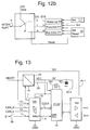
- the device comprises an integrated semiconductor circuit 100, implemented in any technology and design, and an electronically switchable voltage regulator 20 which replaces the voltage regulator usually contained in corresponding electronic devices.
- the semiconductor circuit 100 is figuratively represented here as an integrated component in the conventional sense. So it can also be practically executed. Nevertheless, it can also be a system on a monolithic semiconductor chip, which e.g. as part of a more extensive semiconductor circuit e.g. is deposited in the manner of a standard cell. In any case, the scope of the invention includes, without limitation, all intermediate embodiment forms.
- the semiconductor circuit 100 is connected between the bus wires CAN_H and CAN_L and the bus protocol module 22 assigned to the microcontroller 21 of the electronic device under consideration, thus decouples the latter from the bus CAN_H / CAN_L (hereinafter CAN_H or CAN_L denotes the respective bus wire, CAN_H / CAN_L, however, both wires, ie the bus as a physical two-wire line).
- CAN_H and CAN_L are routed to corresponding connections 11 and 12 of the semiconductor circuit 100.
- the semiconductor circuit 100 in turn is connected to the Tx / Rx communication port of the bus protocol module 22 via a connection path 2 and 3 for data TxD to be sent and data RxD to be received.
- the semiconductor circuit 100 is also connected by further connections 8 and 9 via two terminating resistors 16 and 17 to the corresponding bus wire CAN_H and CAN_L.
- the semiconductor circuit 100 has an input 7 which is connected via a resistor 18 with a logic H potential, for example with a supply potential or a potential which is close to the latter.
- the resistor 18, on the other hand, can be connected to ground GND via a remote switch 25.
- the semiconductor circuit 100 also has at least one for emitting an error and interrupt signal (ERROR or INTERRUPT) at an output 4, which is connected to a correspondingly assigned input of the I / O port 23 and / or a corresponding interrupt input 24 of the Microcontroller 21 is connected, and two vice versa in a corresponding manner from the I / O port 23 of the microcontroller 21 controlled inputs 5 and 6 for a STANDBY signal (STB at input 5) and a TRANSMIT EN ENLE signal (EN on Input 6).
- ERPOR error and interrupt signal
- INTERRUPT error and interrupt signal
- the semiconductor circuit has its power supply 100 a connection 13 to ground GND, further a connection 14 to which the supply potential VBATT - preferably obtained via a polarity reversal protection device 19 from a higher-level supply potential UBATT - is present.
- the semiconductor circuit 100 also has a control output 1 and an input 10, both of which are connected to an electronic voltage regulator 20 which is included in the device and to whose input 20.1 the supply potential VBATT is also conducted.
- the output 20.2 of the controller 20 is connected on the one hand to the aforementioned input 10 of the semiconductor circuit 100 and, in addition, supplies the microcontroller 21 and the bus protocol module 22 as well as the rest of the electronics of the electronic device containing the device, which is indicated in FIG. 13, with operating current a voltage VCC reduced by VBATT by the regulator drop.
- the controller 20 also has an input 20.3 for a (VOLTAGE REGULATOR) ENA BLE or - NOTINH IBIT or NOTENABLE or INHIBIT signal - hereinafter abbreviated ENA / NINH or NENA / INH - which is connected to the Control output 1 of the semiconductor circuit 100 communicates. Furthermore, the controller 20 also has a P O W E R O N R ESET output 20.4 - hereinafter abbreviated PWROR, which communicates via a line 29 with a reset input 28 of the microcontroller 21.
- a (VOLTAGE REGULATOR) ENA BLE or - NOTINH IBIT or NOTENABLE or INHIBIT signal - hereinafter abbreviated ENA / NINH or NENA / INH -
- PWROR P O W E R O N R ESET output 20.4 - hereinafter abbreviated PWROR, which communicates via a line 29 with a reset input 28 of the microcontroller 21.
- the semiconductor circuit 100 is divided here by way of example into four blocks 110, 120, 130 and 140; the feed paths of these blocks required for the internal power supply are omitted in FIG. 2 for reasons of clarity.
- the distribution of detailed functions to these blocks described below is not absolutely mandatory and does not represent a limitation of the invention. Rather, this distribution has proven to be expedient for a first implementation of the semiconductor circuit 100 and will be variable within certain limits depending on different implementation technologies.
- An essential physical function of the semiconductor circuit 100 is the electrical isolation of the bus protocol module 22 from CAN_H and CAN_L, on which surge & load dump transients can occur, which - depending on the manufacturing technology - the bus protocol module 22 (more or less sensitive) may also destroy the entire microcontroller 21).
- the semiconductor circuit 100 can comprise specialized semiconductor means (not described in more detail here), which can preferably be contained in the block 110, in particular means for overvoltage protection against the supply potential rail VBATT. The realization of such means is familiar to the person skilled in the art.
- the block 110 further comprises the means required for the internal power supply of all subfunctions from the supply potential VBATT present at the connection 14 of the semiconductor circuit 100.
- One through the block 140 looped control or switching potential (for the generation of the ENA / NINH signal for the voltage regulator 20) is made available to the block 140 via a path 151.
- block 110 comprises detector means which cause the supply potential VBATT at terminal 14 to drop until a first limit value VL1 (for example 3.5 volts in a motor vehicle) is undershot and preferably also to decrease the controller output potential VCC at terminal 10 until it falls below a second limit value VL2 (for example 1 volt in a motor vehicle), furthermore optionally the simultaneity or chronological sequence of the occurrence of such undershoots.
- the signals from said discriminators are linked by logic means to form a power fail signal which can be transmitted to block 140 via a path 102 and the meaning of which is explained in more detail below.
- block 110 also includes, for example, a wake-up detection logic (WAKEUP logic) 111.
- WAKEUP logic wake-up detection logic
- the above-described connection 7 and the bus wires CAN_H and CAN_L on connections 11 and 12 are connected to this logic.
- This wake-up logic is such that it can convert both an analog wake-up signal or a wake-up signal edge from connection 7 and a wake-up message from the bus into a standardized WAKEUP signal, which is sent via path 103 to block 140 (for Evaluation in function block 145) is output.
- the block 120 preferably comprises all the reading means 121 required for reading the bus, i.e. those for differential and single-wire signal detection, including all error handling and logic means 122, which are required for the bus error-dependent change of the different reading types (e.g. two-wire, single-wire to GND or VCC, and possibly also single-wire to "dead wire” etc.).
- These can preferably include Reference level comparators, wire level comparators and / or sign discriminators include.
- the block 120 can be designed such that it automatically and / or independently in the error-responsive setting and / or reconfiguration and / or adaptation of its receiving means - regardless of the transmission means and their corresponding error-responsive setting and / or reconfiguration and / or adaptation Is location, ie has absolute operational and functional autonomy (full-supported receiver).
- the digital message signal RxD obtained provides downstream logic means 122 both to the connection 3 of the semiconductor circuit 100 and via an internal path 104 to the error signaling module 143 in block 140.
- Block 130 contains all the means related to the signal flow path, which, when implemented, are expediently not assigned to receive block 120 and, in the broadest sense, are assigned to the transmission means in the signal flow path.
- both the receiving and the transmitting means are preferably designed and dimensioned in such a way that - without the need for external protective means - they are autonomously fault-tolerant in relation to all possible error states specific to the application, i.e. cannot be damaged by such.
- the function blocks 131 and 132 or the means thereof, which are located on the bus in addition to the wake-up detection logic 111 and the receiving means 120, or their means are here, for example, assigned to the transmission block 130, which only contains transmission means in the broadest sense; in a narrow sense, transmission means are comprised of 133 (the design details for damage-free fault tolerance which are to be provided as a function of the respectively selected implementation technology of the semiconductor circuit 100 are known per se).
- the block 130 comprises the function block "termination switching means” 131 for switching the high and low impedance of the bus termination as specified by the terminating resistors 16 and 17, a function block 132 "bus error detection means” for discriminating error states on CAN_H / CAN_L, and in particular also short circuits each Bus core according to ground GND or UBATT in the sleep or standby state (SLEEP / STANDBY), as well as transmission means in the form of a fault-tolerant power amplifier 133 in the above sense, which internally contains CAN_H and CAN_L single drivers, which on the output side lead to connections 11 and 12 are.
- Such an output stage can include high and low-side switches, the essential elements of which Switching outputs are connected to the bus wires via coupling diodes.
- the output stage is designed in such a way that it can be set and / or reconfigured and / or adapted (e.g. changing to single-wire operation) depending on the type of bus error that occurs.
- Block 130 also includes means, if necessary.
- the output stage can also be designed such that it is or remains automatically enabled by the CAN_H / CAN-L bus when a defect or intrinsic error occurs in the semiconductor circuit 100, for example by blocking its EN input. Such an activation can be inevitable.
- the power supply to the output stage can also be designed to be switched off automatically, as a result of which a latchup of the bus network due to incorrect current supply to the bus wires is avoided, particularly in the event of errors in the area of the output stage, its input signal path or its status control.
- the above-mentioned coupling diodes can then act as decoupling valves in this context.
- the function block 132 is connected to the function block 131, furthermore to the control block 140. It also communicates with the transmission output stage 133.
- the latter has an on / off input (TRANSMIT- EN ABLE) EN which is connected to the connection 6 of the semiconductor circuit 100 communicates.
- the above-mentioned possibility of forcing the output stage 133 from the CAN_H / CAN_L bus can be implemented, for example, in such a way that the input EN of the output stage 133 can be locked in the event of a defect, so that the transmission signal TxD can no longer affect the bus.
- Such forced activation can also be provided in the event that the potential VBATT and / or VCC falls below a predetermined threshold value, thereby avoiding an undesired inactive burden on the bus.
- Control block 140 also performs several functions. For this purpose, it comprises - as a means for initializing the microcontroller 21 - a controlled switch or a gate 141 for delivery at terminal 1 of 100 of a switch-off or switch-on signal ENA / NINH for the voltage regulator 20, a function block 142 for detecting and setting the "Sleep", “Standby”, “Receive only” and “Normal” operating modes imposed by the microcontroller (corresponding to "Sending and receiving" (SLEEP, STANDBY, RECEIVE ONLY, NORMAL) of the device, and an error signaling module 143.
- SLEEP Send and receiving
- the latter preferably consists of a function block 144 for evaluating bus errors in a (BUS) ERROR INTERRUPT signal and a function block 145 for generating a WAKEUP INTERRUPT signal as a function of a wake-up signal and / or a POWERFAIL INTERRUPT signal as a result a lack of supply as explained in more detail below.
- the block 143 contains, for the generation of these different signals, for example at least three flag flip-flops for a WAKEUP, a POWERFAIL and a BUS ERROR flag; depending on the operating mode, these flags are read out as INTERRUPT.
- the function block 142 has, for example, a two-bit wide port, consisting of input 5 for STB (STANDBY) and input 6 for EN (TRANSMIT- EN ABLE), the latter mentioned with the same marked on / off input the power amplifier 133 is connected.
- STB STB
- EN TRANSMIT- EN ABLE
- the invention is of course not limited to the four operating modes of the semiconductor circuit 100 that can be selected here in binary fashion by two logic levels.
- the function block 142 is also connected to the error signaling module 143, the latter here, for example, a single output ERROR / INTERRUPT led to the connection 4 of 100 - hereinafter also abbreviated ERR / INT - for an error display or interrupt signal and an internal input to which the message signal output by block 120 can be fed via path 104 already mentioned.
- ERR / INT signal at connection 4 can be assigned different meanings.
- At least two designated outputs ERROR and INTERRUPT can also be provided, whose ERROR or INTERRUPT signals then need not be interpreted depending on the operating mode, provided that a correspondingly larger number of connections for the semiconductor circuit 100 can be tolerated.
- a 14-pin DIL pinout for logic circuits for example in the SO-14 housing, is used. This is necessary due to this limitation of the number of connections to a total of fourteen Reinterpretation of the signal that can be taken off at output 4 is shown below with Figen. 12a and 12b explained.
- the voltage regulator 20 By means of the voltage regulator 20, including means, it generates a PWROR signal at its output 20.4 after each switch-on and outputs this via connection 29 to a reset input 28 of the microcontroller 21 in order to ensure its correct initialization after its supply voltage VCC has been built up.
- the controller-microcontroller initialization path is checked for errors.
- the selection bits present at the connections 5 ( ST AND B Y / STB) and 6 (TRANSMIT EN ABLE / EN) select one of the four operating modes SLEEP, STANDBY, RECEIVE ONLY, and NORMAL of the semiconductor circuit 100. These operating modes are used in Within the framework of a higher-level bus management software for operating the bus network, it is managed and explicitly by the application software of the relevant electronic device in which the device is located. initiated.
- the switch or the gate 141 is activated such that the logic signal ENA / NINH output from the control output 1 to the control input 20.3 of the voltage regulator results in the regulator 20 being switched off.
- the logic potential at control output 1 in this operating mode is "L", for example.
- the microcontroller 21 and the bus protocol module 22 have no supply voltage VCC and are therefore de-energized.
- the device In the SLEEP operating mode, the device only has to recognize a defined minimum activity on CAN_H / CAN_L and / or on connection 7 quasi-static wake-up requests, for example from a switch 25, which is preferably designed as a ground contact GND for reasons of power savings, and if necessary, that Generate ENA / NINH signal, therefore needs 30 ... 500 ⁇ A supply current.
- This operating mode is therefore suitable for devices in which a certain amount of time can be tolerated, which elapses between the build-up of the potential VCC and the ignition of the internal clock frequency and the initialization of the watchdog of the microcontroller 21 (order of magnitude 25 ms).
- the input 7 is set to "L" by its actuation, which also uses the wake-up detection logic 111 and the path 103 to control the switch or gate 141 and thus to the same wake-up result leads.
- the NORMAL operating mode can be carried out from the SLEEP operating mode by sensing a WAKEUP request either via the bus - ie by means of the wake-up detection logic 111 - or as a local request by the switch 25.
- the STANDBY operating mode is characterized by that the ENA / NINH signal output by the semiconductor circuit 100 to the voltage regulator 20 switches the latter on or keeps it switched on.
- the supply voltage VCC is therefore also present in the STANDBY mode.
- the STANDBY operating mode is therefore suitable for devices or cases in which the certain amount of time (around 25 ms) that is tolerable in the SLEEP operating mode must not be lost until the bus protocol chip becomes operational. Practical examples of this would be e.g. cylinder neutral travel on a printing press or the infrared remote control of the door lock of a motor vehicle, which require readiness to receive within a very short time in order to avoid inhibitions in response and / or loss of messages.
- the activation of the semiconductor circuit 100 in the operating modes STANDBY, RECEIVE ONLY and NORMAL can be accomplished in three ways overall: from the microcontroller 21 via 4, 5 and 6, by message via CAN_H / CAN_L and by local wake-up request, for example by a switch contact.
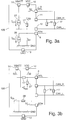
- the function block 131 contains, inter alia, a switch S 1 , which can connect the connection point 8 to ground GND and thereby switch CAN_H to ground via the external terminating resistor 16, a switch S 2 , which connect the connection point 9 to the regulated supply potential VCC and can thereby connect CAN_L to VCC via the external terminating resistor 17, and at least one further switch S 3 which can connect CAN_L to the higher supply potential VBATT via an internal resistor 17 '.
- the switch S 1 are powered by a current source 26 with impressing current I OL and Switch S 3 bridged by a current source 27 with impressing current I OH .
- the currents I OH and I OL are very low and can be of the order of magnitude of, for example, 1 ... 20 ⁇ A.
- the current sources can also be replaced by high-impedance resistances between, for example, 50 ... 250 k ⁇ , as illustrated in FIG. 3b .
- the terminating resistors 16 and 17 are the same and are determined depending on the previously known number of bus users. Normally they can have, for example, 560 ⁇ ⁇ 5% for a larger bus network and a maximum of 15 k ⁇ ⁇ 5% for a small bus network.
- the low impedance in larger bus networks follows on the one hand from the higher capacitive burden of larger networks and on the other hand from the requirement of sufficient suppression of unwanted interference of a static and electromagnetic type in a spatially extensive bus network.
- the internal resistor 17 ' which is preferably integrated in the semiconductor circuit 100, has a value in the order of magnitude of 12 k ⁇ in a bus network which is designed for around 20 subscribers, based on a resistor 17 in the order of magnitude of 600 ⁇ for normal termination. For details on dimensioning, see FIGS. 6 and 7 and the associated description. In practice, an ON resistance of switches S 1 to S 3 can be tolerated up to 200 ⁇ .
- the switch 25 'symbolized in device A symbolizes the electronic switch which, when activated, switches the wire CAN_L from its high recessive level to the active level of CAN_L which is only slightly above ground GND.
- the switch 25 ′ therefore not only acts similarly to the aforementioned switch 25 to ground GND at the local wake-up input 7 of the semiconductor circuit 100. Ultimately, it also becomes effective within the semiconductor circuit as a result of an activation of an external local wake-up switch 25.
- the voltage regulators 20 in the bus subscribers A to n are switched off, as a result of which VCC fails as a termination potential because, due to the absence of VCC, all VCC rails are virtually connected to ground GND inside the device. If CAN_L were terminated by resistors 17 'with a value corresponding to that of resistors 17 and 16 against VCC - in the SLEEP state, therefore, virtually against ground GND - waking via bus CAN_L would not occur, for example, if the CAN_H bus wire was interrupted possible.
- Resistor 17 ' has a considerably larger value here, which corresponds approximately to a multiple corresponding to the expected number n of devices on the bus (for example, approximately 12 kOhm if resistor 17 corresponds to approximately 600 ⁇ in a bus network with approximately 20 participants ).
- this resistor 17 ' is not due to the potential VCC disappearing in the SLEEP operating state (normally approx. 5 volts), but - can be connected via S 3 - to the significantly higher supply potential VBATT (for example approx. 12 volts) which is also available in the SLEEP operating mode. .
- This measure thus changes the source function of the device A waking up in FIG. 6 to one Source function of the multiplicity of all devices B to n to be woken up on the bus, while the waking device A remains a sink function in this regard.
- the voltage curve on the wire CAN_L of the CAN thus closed asymmetrically in the SLEEP state from the beginning at time t 1 of a wake-up process via this wire is illustrated in FIG. 8 .
- the voltage swing on CAN_L has a value V CAN_Li between VCC and VBATT.
- the semiconductor circuit 100 Triggered by the wake-up message via CAN_L (recognizable with this large voltage swing), the semiconductor circuit 100 generates the ENA / NINH signal in each of the subscriber devices A to n lying on the bus, which signal is transmitted on the one hand via the already mentioned function blocks 111 and 140 including switches or Gate 141 turns on all voltage regulators 20 in these devices, making VCC available in each device.
- switch S 3 disconnects the connection between CAN_L and the supply potential VBATT via the high-impedance terminating resistor 17 'and instead connects CAN_L via S 2 through the normal terminating resistor 17 to the lower supply potential VCC. It can thus be seen that at a time t 2 the drop in the voltage swing on the bus via ground GND to a stationary value V CAN_Lstat is completed, the time period (t 2 - t 1 ) essentially being the overall response time of the Semiconductor circuit 100 and the controller 20 to a wake-up signal.
- bus network within one Bus network individual bus participants can remain in the STANDBY mode and others in the SLEEP state. Other bus subscribers could also be woken up by a device in the STANDBY operating mode if the low-side switch of the power amplifier 133 can be activated for this purpose in the sense of the symbolic switch 25 '.
- An example of the use of the STANDBY operating mode is, for example, the (waiting) web feed of a printing press or the infrared receiving part of a locking system of a vehicle, which has to wait uninterruptedly for the arrival of the material feed or coded unlocking signal.
- the controller 20 is switched on in such a device, VCC is consequently present, so that the time consumption (t 2 -t 1 ) until a response via the bus is largely eliminated.
- the function block 131 can also have an operating diagram according to FIG. 3b ; in this case the resistors 17 and 17 'each act in series. To this extent, the resistor 17 'would be effective at the terminal 9 of the semiconductor circuit 100. Fundamental changes in the network analysis according to Figen. 4 to 11, however, not.
- the resistor 26 ′ corresponding to the current source 26 in FIG. 3a can nevertheless be connected to ground GND via a special switch S OT , for example in connection with the automatic adjustment of the level comparison to enable the receiving means 120 and / or the transmitting output stage 133 to perform a test function in the event of a bus error or in the case of external diagnostic measurements on the bus.
- this effect could also be realized by a pinch control of the current source 26.
- FIG. 9 now illustrates the conditions in the wide network in the event of a short circuit of the bus wire CAN_L to ground GND in the “SLEEP” or “STANDBY” operating mode.
- FIG. 10 illustrates the conditions in the network in the event of a short circuit in the bus wire CAN_H with an on-board power rail on UBATT in the operating mode "SLEEP” or "STANDBY” (supply board connection).
- the hard-wired logic of the semiconductor circuit 100 has the effect that the level discriminator or comparator monitoring the short-circuit faulty bus wire is locked within the function block 132 and, as a direct consequence of this switching process, the (local) termination to this bus wire is switched to "short circuit detected", i.e. the current source 26 or 27 or the resistor 26 'or 27' is activated.
- bus error response logic hard-wired in the semiconductor circuit in each individual bus subscriber - with the bus-wide effect of a distributed error handling intelligence in the network - enables the implementation of error response times in the order of one (bus) bit time and below , so that message losses in the course of a bus error-related reconfiguration of the transmitting and receiving components of 100 can be largely or completely avoided. This is a great advantage over all bus master solutions that are centrally aligned on a software basis.
- the already mentioned supply monitoring is also implemented in the semiconductor circuit 100, the purpose and function of which are explained as follows.
- the microcontroller 21 is regularly de-energized. Therefore an initialization of the microcomputer from the de-energized state must be provided, as soon as the controller has reset the microcontroller 21 via its PWROR output 20.4.
- the microcontroller In the case of the example of a motor vehicle, the microcontroller must be able to access incremental data, which were valid at least during the last operation of the motor vehicle and correspond to setting states as found by the user before the new start-up, with each new start-up for example on data relating to the adjustment of adjustable seats, rear-view mirrors, etc.
- voltage level monitors are carried out and evaluated in function block 110, for example in accordance with the following scheme; Without restricting generality, the situation in a motor vehicle and the voltages that occur as an example are used as a basis:
- function block 110 discriminates VBATT with normally 12 volts against a limit value VL1 of, for example, 3.5 volts. In the event that the microcontroller 21 or its watchdog does not have its own power fail detection, it further discriminates VCC with normally 5V against a second limit value VL2 of, for example, 1V (limit voltage for dynamic data seminarability in the RAM of the microcontroller 21).
- a POWERFAIL INTERRUPT signal can be output to 4, which is either only based on a discrimination of VBATT or on a combined discrimination of VBATT and VCC declines. If, in the following, a power fail flag of the semiconductor circuit 100 is mentioned, this does not mean that the microcontroller 21 does not have its own VCC monitoring or does not have any aids that can do this.
- the microcontroller 21 consequently recognizes at its restart after a reset from the absence (not being set) of the power fail flag in function block 145 or 143 with respect to VCC and / or VBATT that neither a re-teaching nor an update of incremental data from its own EEPROM is working so continue with the ones currently in its RAM.
- the power fail flag is read here, for example according to FIG.
- the on-board electrical system voltage UBATT can drop very far from the initial nominal voltage for a short time, namely below VL1, with the result that VBATT also drops correspondingly far, while VCC after initial energization of the controller 20 by virtue of a support capacity arranged downstream of the latter 161 is still held above VL2.
- the supply status VBATT ⁇ VL1 is therefore recognized, but at the same time the supply status VCC> VL2, which prevents the power fail flag from being set in function blocks 145 and 143 (inhibit).
- the INTERRUPT signal at 4 is not output Powerfail for VBATT. From the absence of this interrupt, the microcontroller 21 recognizes that neither a re-learning nor an update of incremental data from its own EEPROM is required and continues to work with the data currently in its RAM.
- microcontroller 21 Does the microcontroller 21 have its own VCC monitoring or such an auxiliary means, i.e. With its own power fail flag, it can recognize from the absence of the external POWERFAIL INTERRUPT at 4 out of 100 and the setting of its own VCC power fail flag that it is not necessary to re-learn incremental data, but the data that is currently to apply , must first be loaded from its EEPROM into its RAM.
- the power fail flag relating to VCC is also set in the microcontroller. This state and the POWERFAIL-INTERRUPT signal at 4 are evaluated by the microcontroller 21 as having been successfully disconnected and reconnected to the terminal 30 supplied with continuous current. As a result, it learns end stops and the relative position (s) of the element it controls when it is restarted and stores it in its EEPROM.
- the requirement can be met that an interruption lasting, for example, 1.5 seconds of the supply potential UBATT without data loss and power fail detection with respect to VCC is possible, however, that after an interruption period of at least 30 seconds, for example, when the microcontroller restarts, a new learning cycle is triggered with regard to the data to be stored incrementally on end stops.
- the scope of the invention is not restricted to the aforementioned exemplary supply monitoring. In this respect, others that differ from the above may also be appropriate depending on the application.
- the semiconductor circuit can have a larger number of connections (for example also when integrated as a standard cell), it can also have additional inputs for selecting various permanently programmed supply monitoring types, which can be selected in accordance with the selection circuitry or control.
- the already mentioned forced activation of the transmission output stage 133 can optionally be provided with the effect that the output stage 133 is separated from CAN-H / CAN_L when the potential VBATT and / or VCC drops below a predetermined threshold value, whereby a burden on the function of the bus is avoided.
- the connection 157 in FIG. 2 symbolizes this aspect.
- the device is connected to UBATT or VBATT at time t 3 .
- the semiconductor circuit 100 outputs the signal ENA / NINH to the control input 20.3 of the controller 20 at the time t 4 at the control output 1.
- the supply voltage VCC of the microcontroller 21 then builds up up to the time t 5 .
- controller 20 emits the PWROR signal for the purpose of resetting microcontroller 21 for initialization.
- the semiconductor circuit 100 - and in particular its function block 110 - can also comprise special means which cause the ENA / NINH signal to initially start when input 14 is charged with VBATT (switching on a control device with the device at UBATT) is generated regardless of the logical status of the EN and STB inputs, so that current can be supplied to the microcontroller 21 in order to read in its EN and STB signals which subsequently control the operating state of the semiconductor circuit 100.
- ERR / INT signal output at 4 by the microcontroller 21 occurs depending on the logic level of the STB and EN signals output by it, and, since these specify the operating mode of the semiconductor circuit, in Depending on their operating modes SLEEP, STANDBY / RECEIVE ONLY and NORMAL, as follows.
- the microcontroller 21 has safely completed its initialization, including the port check, up to the time period t 7 .
- both signals STB and EN on the part of the microcontroller still have the logic level "L", corresponding to a setting of the semiconductor circuit 100 to the SLEEP state .
- the wake-up flag is set in function block 145 or 143.
- An INTERRUPT at 4 in this period is interpreted by the microcontroller 21 as a WAKEUP INTERRUPT.
- the upper switch position for querying the wake-up flip-flop in blocks 145 and 143 corresponds to this case in FIG. 12b .
- the bus error detection 132 can preferably still be inactive by means which are effective, for example, through the rising edge VCC at the connection 10 of the semiconductor circuit 100.
- An INTERRUPT at 4 in this period is interpreted by the microcontroller 21 as a POWERFAIL INTERRUPT. 12b corresponds to the middle switch position for querying the power fail flip-flop in blocks 145 and 143, respectively.
- an electronic device which comprises the device according to the invention can roughly 13 have an overall block diagram.
- a central support capacitance 161 for the potential VCC at the controller output 20.2 a component 162 determining the clock frequency of the microcontroller 21 and an input / output interface as an interface between sensors and actuators and the microcontroller 21 with bus protocol module 22 163 indicated that both VCC and VBATT are powered.
- This illustration shows that the semiconductor circuit 100 can also be understood as an interface between the CAN_H / CAN-L and the microcontroller 21 or the bus protocol module, both with regard to the functions described above and their arrangement in the communication path.
- the semiconductor circuit 100 and in particular its transmission output stage 133 is inherently protected against all possible bus errors and within the scope of the function block 130 the function blocks 131 and 132 allow the bus handling in the event of an error to maintain communication functionality purely in terms of hardware happens with the exclusion of the microcontroller. This means that the microcontroller and the bus protocol function assigned to it can be completely switched off.
- This feature is further supported by an optionally possible design of the transmission means 130 or at least the output stage 133 included therein, in such a way that it automatically disconnects itself from the bus if there is a defect in the semiconductor circuit 100 comprising it. whereby a blockage of the bus network by a device that is disturbed in this way is avoided.
- the means of the semiconductor circuit by virtue of which, in the event of a fault, the detection of the best remaining possibility of emergency communication via the bus and the setting and / or reconfiguration and / or adaptation of the transmission and reception means, are based on analog comparisons the bus wire potentials can act with fixed tolerance windows for these potentials.
- the semiconductor circuit 100 can also include filter elements that are not shown in the figures in this context - in particular with a low-pass characteristic.
- filter elements between connection 7 and the wake-up detection logic 111 and between connections 11 and 12 for CAN_H and CAN_L and the respective inputs of the (autonomous) receive block 120 and the error detection module 132 and / or the bus input of the wake-up Detection logic 111 can be provided.
- the semiconductor circuit 100 can be defined in a library cell (standard cell) which can either be originally or compilably transferred to semiconductor chips in order to generate its physical appearance there using various technologies.
- the scope of the invention further encompasses that the calf conductor circuit 100, together with the microcontroller 21 and / or the bus protocol module 22, is implemented on a single semiconductor chip and both are implemented monolithically, the monolithic circuit thus obtained then being at least two has different areas supplied with energy.
- the device can include special, integrated means which make external protection means superfluous in order to make the receiving and transmitting means on the bus fault-tolerant to the outside in relation to all error states that are possible in practice throughout the bus.
Landscapes
- Engineering & Computer Science (AREA)
- Theoretical Computer Science (AREA)
- General Engineering & Computer Science (AREA)
- Physics & Mathematics (AREA)
- General Physics & Mathematics (AREA)
- Computer Hardware Design (AREA)
- Power Sources (AREA)
- Semiconductor Integrated Circuits (AREA)
- Small-Scale Networks (AREA)
Applications Claiming Priority (2)
| Application Number | Priority Date | Filing Date | Title |
|---|---|---|---|
| DE19611945 | 1996-03-26 | ||
| DE19611945A DE19611945C1 (de) | 1996-03-26 | 1996-03-26 | Einrichtung für den busvernetzten Betrieb eines elektronischen Gerätes mit Microcontroller sowie deren Verwendung |
Publications (2)
| Publication Number | Publication Date |
|---|---|
| EP0798626A1 true EP0798626A1 (fr) | 1997-10-01 |
| EP0798626B1 EP0798626B1 (fr) | 2001-07-11 |
Family
ID=7789486
Family Applications (1)
| Application Number | Title | Priority Date | Filing Date |
|---|---|---|---|
| EP97103932A Expired - Lifetime EP0798626B1 (fr) | 1996-03-26 | 1997-03-10 | Dispositif d'opération en réseau de bus d'un appareil électronique avec un microcontrôleur et méthode de mise en oeuvre |
Country Status (5)
| Country | Link |
|---|---|
| US (1) | US5892893A (fr) |
| EP (1) | EP0798626B1 (fr) |
| JP (1) | JP3217730B2 (fr) |
| KR (1) | KR100252772B1 (fr) |
| DE (2) | DE19611945C1 (fr) |
Cited By (7)
| Publication number | Priority date | Publication date | Assignee | Title |
|---|---|---|---|---|
| WO2002003618A1 (fr) * | 2000-06-30 | 2002-01-10 | Robert Bosch Gmbh | Procede, appareil et gestionnaire de bus pour le fonctionnement d'un appareil raccorde a un reseau de communication automobile |
| EP1295473A1 (fr) * | 2000-06-27 | 2003-03-26 | Thomson Licensing S.A. | Appareil multimedia de reception d'emission audiovisuelle |
| WO2005096124A1 (fr) * | 2004-03-30 | 2005-10-13 | Volkswagen Ag | Procede et dispositif de gestion de reseaux physiquement separes |
| EP1717664B1 (fr) * | 2005-04-20 | 2017-12-13 | Denso Corporation | Circuit informatique |
| CN110830343A (zh) * | 2018-08-09 | 2020-02-21 | 英飞凌科技股份有限公司 | 接口电路 |
| CN111835378A (zh) * | 2020-06-08 | 2020-10-27 | 珠海格力电器股份有限公司 | 一种通讯类型切换电路、方法及空调设备 |
| WO2021239301A1 (fr) * | 2020-05-25 | 2021-12-02 | Robert Bosch Gmbh | Conception de circuit avec une puce de base de système et un pilote can |
Families Citing this family (59)
| Publication number | Priority date | Publication date | Assignee | Title |
|---|---|---|---|---|
| DE19714937A1 (de) * | 1997-04-10 | 1998-10-15 | Bayerische Motoren Werke Ag | Datenbussystem für Kraftfahrzeuge |
| US6075742A (en) * | 1997-12-31 | 2000-06-13 | Stmicroelectronics, Inc. | Integrated circuit for switching from power supply to battery, integrated latch lock, and associated method for same |
| WO1999046888A1 (fr) * | 1998-03-10 | 1999-09-16 | Koninklijke Philips Electronics N.V. | Systeme de transmission de donnees |
| US6182238B1 (en) * | 1998-05-14 | 2001-01-30 | Intel Corporation | Fault tolerant task dispatching |
| DE19904878A1 (de) * | 1999-02-06 | 2000-08-10 | Merten Gmbh & Co Kg Geb | Einrichtung für einen Datenbus |
| DE19918512C1 (de) * | 1999-04-23 | 2000-11-16 | Daimler Chrysler Ag | Schaltungsanordnung mit einer Reduktionsschaltung zur Reduktion von Störlängsspannungen auf einer Zweidrahtleitung |
| DE19947407C2 (de) | 1999-10-01 | 2002-08-01 | Bayerische Motoren Werke Ag | Datenbussystem für Kraftfahrzeuge |
| DE10008081B4 (de) * | 2000-02-22 | 2004-02-05 | Siemens Ag | Serielles Bussystem |
| DE10016173A1 (de) * | 2000-03-31 | 2001-10-04 | Bosch Gmbh Robert | Busstation für ein optisches Bussystem |
| DE10039438C2 (de) * | 2000-08-11 | 2002-06-20 | Infineon Technologies Ag | Zweistufiger Operationsverstärker |
| DE10060539C1 (de) * | 2000-12-06 | 2002-06-20 | Daimler Chrysler Ag | System zur Steuerung oder Regelung |
| FR2829977B1 (fr) * | 2001-09-24 | 2003-12-12 | Valeo Vision | Projecteur d'eclairage ou de signalisation a controleur integre pour vehicule et systeme d'eclairage ou de signalisation equipe d'au moins un tel projecteur |
| DE10155975A1 (de) | 2001-11-14 | 2003-05-28 | Conti Temic Microelectronic | Verfahren zur Überprüfung der fehlerfreien Funktion von Modulen in einem Bussystem mit einer Zentraleinheit sowie entsprechende Module und Zentraleinheit |
| DE10161656A1 (de) * | 2001-12-14 | 2003-06-26 | Bosch Gmbh Robert | Verfahren und Vorrichtung zum bidrektionalen Übertragen von Daten |
| CA2415598A1 (fr) * | 2002-01-11 | 2003-07-11 | Nec Corporation | Systeme et methode de communications multiplex |
| DE10210664C1 (de) * | 2002-03-12 | 2003-08-07 | Daimler Chrysler Ag | Vorrichtung zur Verwaltung von Netzwerken |
| DE10225578A1 (de) * | 2002-06-10 | 2003-12-18 | Philips Intellectual Property | Verfahren und Chipeinheit zum Ansprechen und/oder Aktivieren eines Teilnehmers |
| AU2003263806A1 (en) * | 2002-07-25 | 2004-02-16 | Globespan Virata Incorporated | Methods and systems for improved adsl performance |
| DE10246337B3 (de) * | 2002-10-04 | 2004-05-19 | Daimlerchrysler Ag | Verfahren zum Überwachen von Weckvorgängen bei Datenbussystemen |
| DE10247637B4 (de) * | 2002-10-11 | 2004-09-30 | Audi Ag | Schaltungsanordnung zur Ermittlung eines ein wake-up-Signal sendenden Steuergeräts eines Bus-Systems mit mehreren weiteren Steuergeräten |
| DE10255449A1 (de) * | 2002-11-28 | 2004-06-24 | Daimlerchrysler Ag | Vorrichtung zum Wecken eines Steuergerätes |
| JP4637820B2 (ja) * | 2003-02-13 | 2011-02-23 | エヌエックスピー ビー ヴィ | データバスシステムにおける接地オフセットの補償用配置 |
| US20040195795A1 (en) * | 2003-04-07 | 2004-10-07 | Shih-Ming Huang | Pull catch control device for skateboard |
| DE10330451B3 (de) * | 2003-07-05 | 2004-09-30 | Daimlerchrysler Ag | Vorrichtung zum Wecken eines Steuergerätes |
| CN100472495C (zh) * | 2003-09-09 | 2009-03-25 | 汤姆森许可贸易公司 | 数据总线的有源上拉设备 |
| EP1610384A3 (fr) | 2004-06-14 | 2008-11-19 | Denso Corporation | Unité életctronique avec un substrat où un circuit électronique est fabriqué |
| DE102005009491A1 (de) * | 2005-02-24 | 2006-08-31 | Volkswagen Ag | Transceiver für ein Steuergerät |
| US20060244309A1 (en) * | 2005-04-28 | 2006-11-02 | Claussen Stephen P | Vehicle power and communication bus and system |
| US7890232B2 (en) | 2005-08-23 | 2011-02-15 | Fujitsu Ten Limited | Airbag system |
| JP4900692B2 (ja) * | 2006-11-17 | 2012-03-21 | 株式会社デンソー | 通信装置及び乗員保護装置 |
| DE102008008666B4 (de) * | 2008-02-12 | 2013-03-21 | Continental Automotive Gmbh | Schaltungsanordnung |
| JP2011521600A (ja) * | 2008-05-26 | 2011-07-21 | コーニンクレッカ フィリップス エレクトロニクス エヌ ヴィ | マルチメディア・ソースとマルチメディア・シンクを動作モードからスタンバイ・モードへ及びスタンバイ・モードから動作モードへ切り替える方法 |
| DE102009015197A1 (de) * | 2009-03-31 | 2010-10-14 | Volkswagen Ag | Steuergerät für ein Fahrzeugnetzwerk und Verfahren zum Betreiben eines Fahrzeugnetzwerkes |
| JP5363379B2 (ja) | 2009-05-20 | 2013-12-11 | ルネサスエレクトロニクス株式会社 | 通信システム |
| GB2473142B (en) * | 2009-09-01 | 2017-03-01 | Fisher Rosemount Systems Inc | Integrated bus controller and power supply device for use in a process control system |
| DE102010022560B4 (de) * | 2010-06-02 | 2017-03-23 | Novar Gmbh | Verfahren zum Betreiben einer Gefahrenmeldeanlage |
| US8713343B2 (en) | 2010-08-31 | 2014-04-29 | Denso Corporation | Electronic control apparatus |
| JP2013199223A (ja) | 2012-03-26 | 2013-10-03 | Denso Corp | 車載電子装置 |
| US8904049B2 (en) | 2012-08-23 | 2014-12-02 | Lg Chem, Ltd. | Battery pack monitoring system and method for assigning a binary ID to a microprocessor in the battery pack monitoring system |
| JP5601357B2 (ja) | 2012-09-12 | 2014-10-08 | 株式会社デンソー | 電子制御装置 |
| US9804654B2 (en) * | 2012-12-05 | 2017-10-31 | Google Inc. | Backup power architecture for rack system |
| US9329611B2 (en) * | 2013-12-02 | 2016-05-03 | Nxp B.V. | Power control |
| US9768977B2 (en) * | 2015-07-01 | 2017-09-19 | QUALCOMM Technologies International, Ltd | Low-power can management |
| DE102015222112A1 (de) * | 2015-11-10 | 2017-05-11 | Volkswagen Aktiengesellschaft | Ethernet-Bus, Steuergerät und Verfahren zum Aufwecken eines Steuergeräts eines Ethernet-Busses |
| DE102018203707A1 (de) * | 2018-03-12 | 2019-09-12 | Robert Bosch Gmbh | Sende-/Empfangseinrichtung für ein Bussystem und Betriebsverfahren hierfür |
| DE102018203708A1 (de) * | 2018-03-12 | 2019-09-12 | Robert Bosch Gmbh | Sende-/Empfangseinrichtung für ein Bussystem und Betriebsverfahren hierfür |
| EP3672078A1 (fr) * | 2018-12-18 | 2020-06-24 | Siemens Aktiengesellschaft | Procédé de commande de semi-conducteurs |
| CN115022117B (zh) | 2019-05-03 | 2024-07-23 | 微芯片技术股份有限公司 | 仿真有线局域网中的冲突以及相关系统、方法和设备 |
| KR20200144738A (ko) | 2019-06-19 | 2020-12-30 | 휴렛-팩커드 디벨롭먼트 컴퍼니, 엘.피. | 케이블 연결에 상태에 기초한 소비 전력 저감 |
| CN112423403A (zh) | 2019-08-23 | 2021-02-26 | 微芯片技术股份有限公司 | 检测网络上的冲突 |
| CN112422219B (zh) | 2019-08-23 | 2024-05-24 | 微芯片技术股份有限公司 | 以太网接口和相关系统、方法和设备 |
| CN112422385B (zh) | 2019-08-23 | 2022-11-29 | 微芯片技术股份有限公司 | 用于改进的媒体访问的接口以及相关的系统、方法和设备 |
| CN112415323B (zh) | 2019-08-23 | 2024-07-09 | 微芯片技术股份有限公司 | 诊断网络内的电缆故障 |
| CN112422295B (zh) | 2019-08-23 | 2023-06-13 | 微芯片技术股份有限公司 | 以太网接口及相关系统、方法和设备 |
| CN112422153B (zh) | 2019-08-23 | 2023-04-07 | 微芯片技术股份有限公司 | 检测到共享传输介质处冲突后处理数据接收的方法和系统 |
| WO2021195663A1 (fr) | 2020-03-24 | 2021-09-30 | Microchip Technology Incorporated | Communication de source de réveil d'interface à faible nombre de connexions selon un réveil local et distant 10spe et systèmes, procédés et dispositifs associés |
| GB2598316B (en) * | 2020-08-25 | 2022-11-16 | Ge Aviat Systems Ltd | Control circuit for a power distribution node |
| CN113517061B (zh) * | 2021-07-07 | 2024-09-06 | 广州医软智能科技有限公司 | 一种睡眠模式的控制方法和电子设备 |
| DE102022207475A1 (de) * | 2022-07-21 | 2024-02-01 | Zf Friedrichshafen Ag | Schaltungsanordnung für Kommunikationsschnittstellen und/oder Zündungsschnittstellen innerhalb eines Fahrzeugs zur Ausgabe eines zentralen Wake-up oder Go-to-Sleep-Signales |
Citations (3)
| Publication number | Priority date | Publication date | Assignee | Title |
|---|---|---|---|---|
| WO1990001189A1 (fr) * | 1988-07-28 | 1990-02-08 | Robert Bosch Gmbh | Appareil permettant la commutation definie d'un micro-ordinateur en mode d'attente |
| US5375051A (en) * | 1992-11-13 | 1994-12-20 | Daiblo Research Corporation | Apparatus using serial data line to turn on a transceiver or other device |
| GB2288522A (en) * | 1994-04-11 | 1995-10-18 | Daimler Benz Ag | Monitoring a two-wire bus system for faults |
Family Cites Families (3)
| Publication number | Priority date | Publication date | Assignee | Title |
|---|---|---|---|---|
| US5481253A (en) * | 1992-02-18 | 1996-01-02 | Phelan; Michael D. | Automotive security system |
| JP3377267B2 (ja) * | 1993-12-17 | 2003-02-17 | 株式会社東海理化電機製作所 | 自動車用エンジン始動装置 |
| DE19503460C1 (de) * | 1995-02-03 | 1996-03-07 | Daimler Benz Ag | Fehlertolerante Endstufe für ein digitales Zweileiterbus-Datenkommunikationssystem |
-
1996
- 1996-03-26 DE DE19611945A patent/DE19611945C1/de not_active Expired - Fee Related
-
1997
- 1997-03-10 DE DE59703988T patent/DE59703988D1/de not_active Expired - Lifetime
- 1997-03-10 EP EP97103932A patent/EP0798626B1/fr not_active Expired - Lifetime
- 1997-03-25 JP JP11000097A patent/JP3217730B2/ja not_active Expired - Fee Related
- 1997-03-25 KR KR1019970010170A patent/KR100252772B1/ko not_active Expired - Fee Related
- 1997-03-26 US US08/825,027 patent/US5892893A/en not_active Expired - Lifetime
Patent Citations (3)
| Publication number | Priority date | Publication date | Assignee | Title |
|---|---|---|---|---|
| WO1990001189A1 (fr) * | 1988-07-28 | 1990-02-08 | Robert Bosch Gmbh | Appareil permettant la commutation definie d'un micro-ordinateur en mode d'attente |
| US5375051A (en) * | 1992-11-13 | 1994-12-20 | Daiblo Research Corporation | Apparatus using serial data line to turn on a transceiver or other device |
| GB2288522A (en) * | 1994-04-11 | 1995-10-18 | Daimler Benz Ag | Monitoring a two-wire bus system for faults |
Cited By (10)
| Publication number | Priority date | Publication date | Assignee | Title |
|---|---|---|---|---|
| EP1295473A1 (fr) * | 2000-06-27 | 2003-03-26 | Thomson Licensing S.A. | Appareil multimedia de reception d'emission audiovisuelle |
| WO2002003618A1 (fr) * | 2000-06-30 | 2002-01-10 | Robert Bosch Gmbh | Procede, appareil et gestionnaire de bus pour le fonctionnement d'un appareil raccorde a un reseau de communication automobile |
| US7158869B2 (en) | 2000-06-30 | 2007-01-02 | Robert Bosch Gmbh | Method,device and bus manager for operating a device that is connected to a motor vehicle communications network |
| WO2005096124A1 (fr) * | 2004-03-30 | 2005-10-13 | Volkswagen Ag | Procede et dispositif de gestion de reseaux physiquement separes |
| EP1717664B1 (fr) * | 2005-04-20 | 2017-12-13 | Denso Corporation | Circuit informatique |
| CN110830343A (zh) * | 2018-08-09 | 2020-02-21 | 英飞凌科技股份有限公司 | 接口电路 |
| CN110830343B (zh) * | 2018-08-09 | 2022-11-04 | 英飞凌科技股份有限公司 | 接口电路 |
| WO2021239301A1 (fr) * | 2020-05-25 | 2021-12-02 | Robert Bosch Gmbh | Conception de circuit avec une puce de base de système et un pilote can |
| CN111835378A (zh) * | 2020-06-08 | 2020-10-27 | 珠海格力电器股份有限公司 | 一种通讯类型切换电路、方法及空调设备 |
| CN111835378B (zh) * | 2020-06-08 | 2024-03-08 | 珠海格力电器股份有限公司 | 一种通讯类型切换电路、方法及空调设备 |
Also Published As
| Publication number | Publication date |
|---|---|
| KR970068366A (ko) | 1997-10-13 |
| JP3217730B2 (ja) | 2001-10-15 |
| DE19611945C1 (de) | 1997-11-20 |
| KR100252772B1 (ko) | 2000-04-15 |
| EP0798626B1 (fr) | 2001-07-11 |
| DE59703988D1 (de) | 2001-08-16 |
| JPH10105309A (ja) | 1998-04-24 |
| US5892893A (en) | 1999-04-06 |
Similar Documents
| Publication | Publication Date | Title |
|---|---|---|
| EP0798626B1 (fr) | Dispositif d'opération en réseau de bus d'un appareil électronique avec un microcontrôleur et méthode de mise en oeuvre | |
| EP0798895B1 (fr) | Circuit de commutation intégré pour le couplage d'un contrôleur micro-contrôlé au bus à deux fils | |
| DE19611942C2 (de) | Halbleiterschaltkreis für ein elektronisches Steuergerät | |
| DE19513939C2 (de) | Steuervorrichtung zum Steuern von mindestens einer Einrichtung eines Fahrzeugs und Verfahren zum Betrieb einer Steuervorrichtung | |
| DE69107100T2 (de) | Steuerschaltung für die Energieversorgung einer Mehrzahl elektronischer Module. | |
| DE19714937A1 (de) | Datenbussystem für Kraftfahrzeuge | |
| EP2059416B1 (fr) | Gestion de communication par bus sur un vehicule automobile comprenant plusieurs modules de commande relies par un bus | |
| DE102009041434A1 (de) | Verfahren und Vorrichtung zum Aufwecken von Teilnehmern eines Bussystems und entsprechender Teilnehmer | |
| WO2010112173A2 (fr) | Boîtier de commande pour un réseau de bord de véhicule et procédé pour faire fonctionner un réseau de bord de véhicule | |
| EP0775406B1 (fr) | Systeme de transmission de donnees a surete integree, par l'intermediaire d'un bus differentiel | |
| EP0940950A2 (fr) | Interface nodale dans un réseau de données | |
| DE102004026383B4 (de) | Kraftfahrzeug mit mindestens einem von einem Prozessor gesteuerten Steuergerät | |
| DE10330451B3 (de) | Vorrichtung zum Wecken eines Steuergerätes | |
| DE69130720T2 (de) | Stromversorgung für Datenverarbeitungsgerät | |
| DE10223773A1 (de) | Schaltungsanordnung und Verfahren zur Überwachung eines Mikrocontrollers | |
| WO2017017092A1 (fr) | Consommateur électrique pour un véhicule automobile | |
| EP0240833A1 (fr) | Dispositif de surveillance pour la surveillance du fonctionnement de dispositifs de transmission de la technique de transmission d'informations | |
| EP2359215A1 (fr) | Appareil de terrain pour la détermination et/ou la surveillance d'une grandeur physique ou chimique d'un processus | |
| EP2176938B1 (fr) | Appareil de commande électronique destiné à être employé dans un véhicule | |
| DE102005061967B9 (de) | Leistungsversorgungsanordnung zum Bereitstellen eines Ausgangssignals mit einem vorbestimmten Ausgangssignalpegel | |
| DE19523031A1 (de) | System zum Übertragen von Daten über einen differentiellen Bus | |
| DE102004060007B4 (de) | Datenbussystem für Kraftfahrzeuge und Diagnoseverfahren | |
| EP1192551B1 (fr) | Interface pour coupler un noeud de bus a la ligne bus d'un systeme bus | |
| EP1915653A1 (fr) | Dispositif de commande et dispositif de reglage pour une automobile | |
| EP0852764A1 (fr) | Systeme de transmission de donnees |
Legal Events
| Date | Code | Title | Description |
|---|---|---|---|
| PUAI | Public reference made under article 153(3) epc to a published international application that has entered the european phase |
Free format text: ORIGINAL CODE: 0009012 |
|
| AK | Designated contracting states |
Kind code of ref document: A1 Designated state(s): DE ES FR GB IT SE |
|
| RAP1 | Party data changed (applicant data changed or rights of an application transferred) |
Owner name: DAIMLER-BENZ AKTIENGESELLSCHAFT |
|
| 17P | Request for examination filed |
Effective date: 19980228 |
|
| RAP1 | Party data changed (applicant data changed or rights of an application transferred) |
Owner name: DAIMLERCHRYSLER AG |
|
| GRAG | Despatch of communication of intention to grant |
Free format text: ORIGINAL CODE: EPIDOS AGRA |
|
| GRAG | Despatch of communication of intention to grant |
Free format text: ORIGINAL CODE: EPIDOS AGRA |
|
| GRAH | Despatch of communication of intention to grant a patent |
Free format text: ORIGINAL CODE: EPIDOS IGRA |
|
| 17Q | First examination report despatched |
Effective date: 20001130 |
|
| GRAH | Despatch of communication of intention to grant a patent |
Free format text: ORIGINAL CODE: EPIDOS IGRA |
|
| GRAA | (expected) grant |
Free format text: ORIGINAL CODE: 0009210 |
|
| ITF | It: translation for a ep patent filed | ||
| AK | Designated contracting states |
Kind code of ref document: B1 Designated state(s): DE ES FR GB IT SE |
|
| REF | Corresponds to: |
Ref document number: 59703988 Country of ref document: DE Date of ref document: 20010816 |
|
| GBT | Gb: translation of ep patent filed (gb section 77(6)(a)/1977) |
Effective date: 20010830 |
|
| PG25 | Lapsed in a contracting state [announced via postgrant information from national office to epo] |
Ref country code: SE Free format text: LAPSE BECAUSE OF FAILURE TO SUBMIT A TRANSLATION OF THE DESCRIPTION OR TO PAY THE FEE WITHIN THE PRESCRIBED TIME-LIMIT Effective date: 20011011 |
|
| ET | Fr: translation filed | ||
| REG | Reference to a national code |
Ref country code: GB Ref legal event code: IF02 |
|
| PG25 | Lapsed in a contracting state [announced via postgrant information from national office to epo] |
Ref country code: ES Free format text: LAPSE BECAUSE OF FAILURE TO SUBMIT A TRANSLATION OF THE DESCRIPTION OR TO PAY THE FEE WITHIN THE PRESCRIBED TIME-LIMIT Effective date: 20020131 |
|
| PLBI | Opposition filed |
Free format text: ORIGINAL CODE: 0009260 |
|
| PLBQ | Unpublished change to opponent data |
Free format text: ORIGINAL CODE: EPIDOS OPPO |
|
| PLBF | Reply of patent proprietor to notice(s) of opposition |
Free format text: ORIGINAL CODE: EPIDOS OBSO |
|
| PLBF | Reply of patent proprietor to notice(s) of opposition |
Free format text: ORIGINAL CODE: EPIDOS OBSO |
|
| 26 | Opposition filed |
Opponent name: VOLKSWAGEN AG Effective date: 20020411 Opponent name: VALEO SCHALTER UND SENSOREN GMBH Effective date: 20020411 |
|
| PLBP | Opposition withdrawn |
Free format text: ORIGINAL CODE: 0009264 |
|
| PLBP | Opposition withdrawn |
Free format text: ORIGINAL CODE: 0009264 |
|
| PLBD | Termination of opposition procedure: decision despatched |
Free format text: ORIGINAL CODE: EPIDOSNOPC1 |
|
| PLBM | Termination of opposition procedure: date of legal effect published |
Free format text: ORIGINAL CODE: 0009276 |
|
| STAA | Information on the status of an ep patent application or granted ep patent |
Free format text: STATUS: OPPOSITION PROCEDURE CLOSED |
|
| 27C | Opposition proceedings terminated |
Effective date: 20050915 |
|
| REG | Reference to a national code |
Ref country code: FR Ref legal event code: CD Ref country code: FR Ref legal event code: CA |
|
| PGFP | Annual fee paid to national office [announced via postgrant information from national office to epo] |
Ref country code: IT Payment date: 20100324 Year of fee payment: 14 Ref country code: FR Payment date: 20100402 Year of fee payment: 14 |
|
| PGFP | Annual fee paid to national office [announced via postgrant information from national office to epo] |
Ref country code: GB Payment date: 20100322 Year of fee payment: 14 |
|
| GBPC | Gb: european patent ceased through non-payment of renewal fee |
Effective date: 20110310 |
|
| REG | Reference to a national code |
Ref country code: FR Ref legal event code: ST Effective date: 20111130 |
|
| PG25 | Lapsed in a contracting state [announced via postgrant information from national office to epo] |
Ref country code: FR Free format text: LAPSE BECAUSE OF NON-PAYMENT OF DUE FEES Effective date: 20110331 |
|
| PG25 | Lapsed in a contracting state [announced via postgrant information from national office to epo] |
Ref country code: IT Free format text: LAPSE BECAUSE OF NON-PAYMENT OF DUE FEES Effective date: 20110310 Ref country code: GB Free format text: LAPSE BECAUSE OF NON-PAYMENT OF DUE FEES Effective date: 20110310 |
|
| PGFP | Annual fee paid to national office [announced via postgrant information from national office to epo] |
Ref country code: DE Payment date: 20160531 Year of fee payment: 20 |
|
| REG | Reference to a national code |
Ref country code: DE Ref legal event code: R071 Ref document number: 59703988 Country of ref document: DE |