EP0798662A2 - Appareil d'impression et méthode de contrÔle - Google Patents
Appareil d'impression et méthode de contrÔle Download PDFInfo
- Publication number
- EP0798662A2 EP0798662A2 EP97105154A EP97105154A EP0798662A2 EP 0798662 A2 EP0798662 A2 EP 0798662A2 EP 97105154 A EP97105154 A EP 97105154A EP 97105154 A EP97105154 A EP 97105154A EP 0798662 A2 EP0798662 A2 EP 0798662A2
- Authority
- EP
- European Patent Office
- Prior art keywords
- bits
- clock signal
- data
- serial
- dot
- Prior art date
- Legal status (The legal status is an assumption and is not a legal conclusion. Google has not performed a legal analysis and makes no representation as to the accuracy of the status listed.)
- Granted
Links
Images


Classifications
-
- G—PHYSICS
- G06—COMPUTING OR CALCULATING; COUNTING
- G06K—GRAPHICAL DATA READING; PRESENTATION OF DATA; RECORD CARRIERS; HANDLING RECORD CARRIERS
- G06K15/00—Arrangements for producing a permanent visual presentation of the output data, e.g. computer output printers
- G06K15/02—Arrangements for producing a permanent visual presentation of the output data, e.g. computer output printers using printers
- G06K15/10—Arrangements for producing a permanent visual presentation of the output data, e.g. computer output printers using printers by matrix printers
-
- G—PHYSICS
- G06—COMPUTING OR CALCULATING; COUNTING
- G06K—GRAPHICAL DATA READING; PRESENTATION OF DATA; RECORD CARRIERS; HANDLING RECORD CARRIERS
- G06K2215/00—Arrangements for producing a permanent visual presentation of the output data
- G06K2215/0002—Handling the output data
- G06K2215/0077—Raster outputting to the print element(s)
Definitions
- the invention relates to printing apparatuses such as dot-matrix printers. More particularly the invention relates to printing apparatuses in which printing is achieved by means of dot printing elements disposed in a zigzag arrangement.
- impact-type dot printers and non-impact-type dot printers use a print head which has a number of dot printing elements for printing individual dots.
- the printing elements are typically wires while they are ink ejection nozzles in ink-jet printers.
- printing is achieved by driving these printing elements in synchronism with a relative motion of the print head relative to a recording medium (e.g. paper).
- An image is printed by selectively printing individual dots in a dot matrix, i.e., a matrix of possible dot positions.
- the matrix is composed of one or more lines of dot columns.
- Each dot column comprises a number of dot positions corresponding to the number of printing elements of the printer.
- a line is printed by successively moving the print head relative to a recording medium in a first or line direction, and plural lines are printed by successively moving the print head relative to the recording medium in a second or column direction perpendicular to the first direction.
- all printing elements of a print head are arranged in a single row extending perpendicular to the line direction, all dot positions of a particular dot column can be printed at once.
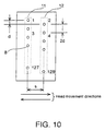
- Fig. 10 illustrates an example of such zigzag arrangement.
- Fig. 10 While the general way of printing an image by means of such print head is well known to those skilled in the art, a brief explanation may facilitate the understanding of the present invention.
- the print head moves from left to right of the line direction and the position of row 12 represents the start of a line, i.e., the position of the first dot column of that line. Because the two rows are spaced apart by s dot columns, row 11 is positioned s dot columns left of the first dot column. Therefore, only the even-numbered dot positions of the first dot column can initially be printed by driving the nozzles of row 12. The print head is then moved stepwise to the right successively printing only the even-numbered dot positions of dot columns 2 to s.
- row 11 is at the position of the first dot column while row 12 is at the position of the ( s + 1)-st dot column. While the even-numbered dot positions of the ( s + 1)-st dot column are printed by the nozzles in row 12, the nozzles in row 11 can now complete the first dot column by printing its odd-numbered dot positions.
- each dot column is printed in a number of steps corresponding to the number of rows of dot printing elements. The delay between these steps depends on the distance (expressed in number of dot columns) between adjacent ones of the rows.
- Fig. 9 illustrates a prior art example of a drive circuit suitable for driving the nozzles 8 arranged as shown in Fig. 10.
- Image buffer 20 holds the printing data in a bit-mapped form, i.e., each bit represents a certain dot position of the image to be printed by the print head.
- Printing data are read from image buffer 20 in units of dot columns, i.e. parallel data words of a number of bits equal to the number k of printing elements of the print head. Since, as explained above, the individual dot positions of a certain dot column cannot not be printed all at once, each data word read from image buffer 20 must be separated into subunits. Each subunit includes the data for the nozzles of a respective one of the two rows 11 and 12.
- the data word (the n -th data word) for the dot column corresponding to the current position of row 11 or 12, whichever is to be printed first depending on the direction of the head's movement, is read from image buffer 20 and then converted into a serial bit string by parallel-to-serial (P/S) converter 25.
- Separation circuit 18 receives the bit string and separates it into substrings of the even-numbered bits and the odd-numbered bits, respectively.
- the substring for the nozzles of the row to be printed first leg., row 11) is converted back to a parallel word (subword) by serial-to-parallel (S/P) converter 13.
- the other substring is applied to a delay circuit 19 in the form of a shift register.
- the shift register delays the other substring by s x 64 bits and applies the delayed substring to S/P-converter 14.
- the subwords from S/P-converters 13 and 14 are simultaneously latched into latch circuits 15 and 16, respectively, and the nozzles of row 11 are driven based on the bits latched in latch circuit 15 while at the same time the nozzles of row 12 are driven based on the bits latched in latch circuit 15.
- the nozzles of row 11 print the odd-numbered dot positions of the n -th dot column
- the nozzles of row 12 print the even-numbered dot positions of the ( n - s )-th dot column where the printing direction is assumed to be from right to left in Fig. 10. If the printing direction is from left to right in Fig. 10, the data for the odd-numbered nozzles must be delayed.
- the prior art requires a the delay circuit 19, a ( s x k /2)-bit shift register, and a circuit for controlling this shift register. Furthermore, to print in both directions of the print head's reciprocating motion in the line direction, both the connection between delay circuit 19 and separation circuit 18 and the connection between delay circuit 19 and either S/P-converter 13 or S/P-converter 14 must be switched depending on the direction.
- an objective of the present invention is to provide a printing apparatus with a print head having dot printing elements in a zigzag arrangement in order to provide high-resolution printing, which employs a simple drive circuit capable of printing bit-mapped data without using the aforementioned delay circuit and/or complicated switching control.
- each time data are read from the image buffer for driving the dot printing elements of the print head a batch of data words is read, the batch comprising i data words when the dot printing elements are arranged in i rows.
- Each data word of the batch includes the bits required for driving the dot printing elements in a respective one of the i rows.
- Reading the i data words as a batch means that all i data words are read either simultaneously or one after the other but without any data word other than one of the i data words being read in between.
- the required bits of each of the i data words are extracted either simultaneously or sequentially and then used to drive all dot printing elements in accordance with the respective ones of the extracted bits at the same time.
- the present invention can eliminate switching control and buffer or delay circuits. Furthermore, since it is not necessary to change the control method depending on the moving direction of the print head, the control can be drastically simplified and the area occupied by the control circuit can be reduced.
- the dot printing elements of one row can print either the odd- or the even-numbered bits, and those of the other row can print the even-numbered or the odd-numbered bits, respectively.
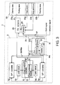
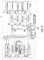
- Fig. 1 is a block diagram of the drive circuit of a printer 1 embodying the present invention. As indicated by the broken line in Fig. 1, part of the drive circuit is provided on the print head 5.
- Image buffer 20 stores printing data 21 in a bit-mapped form to which characters and symbols to be printed have been expanded in a manner well known in the art. As explained above, image buffer is organized to store k -bit data words, i.e., each data word corresponds to one dot column of the image (text or graphic) to be printed.
- Image buffer 20 in this embodiment additionally holds dummy data words 22a and 22b which correspond to at least the s dot columns beyond the first and the last effective dot column in each line.
- the bits of the dummy data words 22a and 22b are L bits, i.e., represent blanks. It is possible to provide dummy data words 22 in a specified area of image buffer 20 beforehand, but it is also possible to automatically generate dummy data words 22 and append them to either end of the data words for one line when the information to printed is converted into the bit-mapped printing data.
- Data words read from image buffer 20 are applied via selector 29 to P/S-converter 25.
- P/S-converter 25 supplies the respective serial bit strings to print head 5.
- a characteristic feature of the present invention in this embodiment is that data words are read in pairs from image buffer 20, the two data words of each pair corresponding to two dot columns spaced apart by s dot columns. Under the control of selection signal 37 selector 29 first selects one and then the other data word of each pair so as to apply them sequentially to P/S-converter 25, one immediately following the other.
- nozzle row 11 for example, is at a position on the left side of the left edge of a particular line, a dummy data word 22a is sent to odd-numbered nozzles in row 11.
- a printing data word 21 is printed by even-numbered nozzles 8 in row 12 only and not by the nozzles in row 11.
- selector 29 always receives a pair of data words (printing or dummy data words) and there is no need to identify the edges of the lines.
- This configuration significantly simplifies the line edge processing in a printer with nozzles in a zigzag arrangement.
- the drive circuit part of print head 5 comprises S/P-converters 13 and 14 and latch circuits 15 and 16 similar to those in the drive circuit shown in Fig. 9 and explained above.
- a clock control circuit 30 is additionally provided.
- Clock control circuit 30 receives clock signal 35 of frequency f used to clock P/S-converter 25, and includes frequency divider 31 for frequency dividing clock signal 35 by 2.
- Selector 32 receives the divided clock signal of frequency f /2 and applies it in response to selection signal 37 either as a second clock signal 36 to S/P-converter 14 or a third clock signal 36a to S/P-converter 13.
- P/S-converter 25 begins converting the data word n + s (the data word corresponding the ( n + s )-th dot column) into a corresponding serial bit string.
- P/S-converter 25 is clocked by clock signal 35 at frequency f, and sequentially supplies bits 1 through 128 to S/P-converters 13 and 14.
- clock signal 36 of frequency f /2 is supplied to S/P-converter 14 and only the even-numbered bits 2 through 128 are extracted to enter S/P-converter 14. Note that clock signal 36 is synchronized with the falling edges of clock signal 35 and is supplied to S/P-converter 14 when P/S-converter 25 begins conversion at the timing shown in Fig. 2.
- the bits of data word n + s which are to be printed by the even-numbered nozzles are separated from those to be printed by the odd-numbered nozzles. Since, during this process, the third clock signal 36a is not supplied to S/P-converter 13 the odd-numbered bits of data word n + s are not entered into S/P-converter 13.
- P/S-converter 25 When P/S-converter 25 has finished sending the last bit of data word n + s , i.e., bit 128 in this embodiment, it starts converting data word n at time t2. During this transition, one period of clock signal 35 is left between the last bit of data word n + s and the first bit of data word n so that now the phase of the divided clock signal from divider 31 is shifted by one bit relative to the bit string from P/S-converter 25. Consequently, when the selection signal causes selector 32 to supply this divided clock signal as the third clock signal 36a to S/P-converter 13, odd-numbered bits of data word n are extracted. After conversion to a parallel subword these odd-numbered bits are used to drive the nozzles of row 11.
- Printer 1 of this embodiment achieves high-resolution printing by repeating the step of sending the data of data words corresponding to each nozzle row position and printing.
- the circuit for sending data from the image buffer to the print head is implemented using an extremely simple circuit in which a P/S-converter for converting the data from the image buffer from parallel to serial is connected to an S/P-converter for converting data from serial to parallel at the print head. Consequently, extra buffer or delay circuits for temporarily storing the data of individual nozzle rows are not needed, nor is it necessary to switch control based on the printing direction of the print head.
- blank dummy data 22 are provided in image buffer 20, a process such as stopping the printing by one of the nozzle rows at the line edge is unnecessary.
- the print head can be made smaller and lighter in weight, and a high-speed compact printer offering excellent printing quality is provided.
- a second embodiment of the invention will be explained with reference to Figs. 3 and 4.
- the second embodiment differs from the first embodiment in that clock control circuit 30a of the second embodiment is additionally provided with inverter 33 that generates a third clock signal 36a by inverting the divided clock signal from divider 31, and that S/P-converter 14 does not receive its serial input signal directly from P/S-converter 25 but through S/P-converter 13.
- selector 32 selectively supplies either the second clock signal 36 or the third clock signal 36a to both S/P-converters 13 and 14.
- P/S-converter 25 begins converting the data word n + s into a corresponding serial bit string.
- the second clock signal 36 is supplied from clock control circuit 30a to both S/P-converters 13 and 14. Based on this second clock signal, the even-numbered bits are extracted and entered into S/P-converter 13.
- the data subword previously held by S/P-converter 13 is successively shifted into S/P-converter 14.
- bit 128 which is the last even-numbered bit of bit string n + s , has been sent to S/P-converter 13 (time t2 in Fig.
- the data word n is converted by P/S-converter 25 into a corresponding serial bit string, immediately following the bit string n + s .
- Bit string n is applied to S/P-converter 13.
- the third clock signal 36a (the phase-inverted version of the second clock signal 36) is supplied from clock control circuit 30a to both S/P-converters 13 and 14. Based on this third clock signal 36a, odd-numbered bits of bit string n are extracted and sequentially entered into S/P-converter 13. Simultaneously, the even-numbered bits of bit string n + s are sequentially put out from S/P-converter 13 and entered into S/P-converter 14.
- both of the first and second embodiments can use either way of creating the phase shift required for selectively extracting the even-numbered bits or the odd-numbered bits.
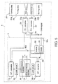
- FIG. 5 A third embodiment of the invention will be explained with reference to Fig. 5.
- the third embodiment differs from the first embodiment in that clock control circuit 30b of the third embodiment includes inverter 33 of the second embodiment but not selector 32.
- this embodiment employs two P/S-converters 26 and 27 operating in parallel, and does not need selector 29. Selection signal 37 is not used, correspondingly.
- Pairs of a data word (23a or 22a) corresponding to the position of the odd-numbered nozzles in row 11 and a data word (23b or 22b) corresponding to the position of the even-numbered nozzles in row 12 are read out in parallel as data words n and n + s from image buffer 20 and applied to P/S-converter 26 and P/S-converter 27, respectively.
- the corresponding two serial bit strings generated from P/S-converters 26 and 27 are applied to S/P-converters 13 and 14, respectively.
- S/P-converter 14 receives the second clock signal 36 and S/P-converter 13 the third clock signal 36a which is phase-inverted with respect to the second clock signal 36, from clock control circuit 30b.
- S/P-converter 14 extracts the even-numbered bits from the bit string resulting from data word n + s and S/P-converter 13 extracts the odd-numbered bits from the bit string resulting from data word n .
- both data word n and data word n + s are simultaneously converted to the respective serial bit string and are sent to the print head. These two bit strings are also simultaneously converted back to parallel subwords by S/P-converters 13 and 14 of print head 5. Consequently, the processing time required for data transfer can be reduced further.
- two serial bit strings each including all the bits of the respective data words are sent either simultaneously or sequentially to the print head 5.
- the drive circuit part of the print head extracts the needed bits from each bit string by using clock signals of half the clock rate of the bit strings and an appropriate phase so as to obtain the even-numbered bits of one bit string and the odd-numbered bits of the other bit string.
- the clock signals 36 and 36a for extracting the even- and odd-numbered bits are virtually phase inverted with respect to each other. More exactly, the phase of the third clock signal 36a relative to the respective one serial bit string is shifted by one clock period of the clock signal 35, i.e., one bit of the bit string, relative to the phase of the second clock signal 36 relative to the respective other serial bit string.
- this phase shift need not be exactly one clock period of clock signal 35 but may a fraction of one period as long as the required bit extraction is achieved.
- bit extraction is achieved by cooperative functions of drive circuit parts on the printer main part and the print head, i.e., parallel-to-serial conversion at a first clock rate on the printer main part side and serial-to-parallel conversion at a second clock rate, which is half the first clock rate, on the print head side.
- the principle of the invention may also be implemented by performing the bit extraction completely on the printer main part side and transferring only the required bits to the print head. This allows for a further simplification of the drive circuit part on the print head side.
- a fourth embodiment of the invention will be explained with reference to Fig. 6.
- the fourth embodiment differs from the first embodiment (compare Figs. 1 and 6) in the following.
- P/S-converter 25 and selector 29 of the first embodiment two P/S-converters 26 and 27, two latch circuits 46 and 47 and two counters 49 and 50 are used.
- the drive circuit part of the print head has no clock control circuit.
- Data words are read from image buffer 20 in pairs of data word n and data word n + s as has been explained for the preceding embodiments.
- the two data words of each pair may be read simultaneously into latch circuits 47 and 46, respectively.
- Each latch circuit has a capacity of k bits (remember k is the total number of nozzles and the length of each data word) and a parallel input and parallel output.
- P/S-converters 26 and 27 have a k/ 2-bit input each. For example, in the printer of this embodiment, P/S-converters 26 and 27 can each convert 64 ( k /2) bits of parallel data to a serial bit string.
- the k /2-bit parallel input of P/S-converter 26 is connected to only the odd-numbered bits of the k bit output of latch circuit 46.
- the k /2-bit parallel input of P/S-converter 27 is connected to only the even-numbered bits of the k bit output of latch circuit 47. It is also possible to mask the odd/even-numbered bits of the k bits in latch circuit 46/47 and supply the result to P/S-converter 26/27.
- P/S-converter 26 converts only the odd-numbered bits of data word n , and sends the resulting serial substring n to S/P-converter 13.
- S/P-converter 13 converts this serial substring into a parallel subword, and controls the odd-numbered nozzles in row 11 via latch circuit 15.
- P/S-converter 27 converts only the even-numbered bits of data word n + s and sends the resulting serial substring to S/P-converter 14.
- S/P-converter 14 converts this serial substring to a parallel subword and controls the even-numbered nozzles in row 12 via latch circuit 14.
- counters 49 and 50 which output k /2 pulses each based on clock signal 35 when trigger signals 39, 40 are received.
- data word n is first set in latch circuit 46.
- counter 49 which controls odd-numbered nozzles of row 11 begins counting based on clock signal 35 and outputs k /2 pulses to P/S-converter 26.
- the odd-numbered-bits of data word n are output at the rate or frequency of clock signal 35 as a serial substring.
- the pulses output by counter 49 are also supplied to S/P-converter 13 which takes in the k /2 bits of the serial substring synchronized with the pulses from counter 49.
- Counter 50 operates in response to even trigger signal 40 in the same way as counter 49 to control P/S-converter 27 and S/P-converter 14 correspondingly.
- the data subwords to be set in latch circuits 15 and 16 on the print head side are available on the printer main part side.
- the reason why they are sent as serial substrings to the print head and reconverted to parallel subwords on the print head side, is that transferring parallel data to the print head would require a correspondingly high number of lines between the print head and the printer main part. This is undesirable where the print head is moveable with respect to the printer main part.
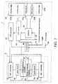
- a fifth embodiment of the invention will be explained with reference to Fig. 7.
- the fifth embodiment may be considered as a combination between the second and the fourth embodiments. More particularly, as shown in Fig. 7, the printer in this embodiment has selector 29 which is used to selectively apply data word n (23a or 22a) and data word n + s (23b or 22b) from image buffer 20 to a single latch circuit 45 which in turn supplies subwords to P/S-converter 25.
- P/S-converter 25 sends a serial substring corresponding to each subword to S/P-converter 13 of print head 5.
- S/P-converter 14 is connected to S/P-converter 13 like in the second embodiment and receives serial substrings from P/S-converter 25 via S/P-converter 13.
- Converters 13, 14 and 25 are clocked by the same pulse signals supplied from counter 48.
- Counter 48 begins counting in response to a trigger signal 41, and outputs k /2 pulse signals at the rate or frequency of clock signal 35.
- Trigger signal 41 is also supplied to latch circuit 45 which supplies data to P/S-converter 25 upon receiving trigger signal 41.
- Latch circuit 45 is a k -bit register responsive to selection signal 42 for selectively applying either only the even-numbered bits or the odd-numbered bits to P/S-converter 25 having a k /2-bit parallel input. This kind of control can be easily implemented using a data selector.
- selection signal 42 is first set to select even-numbered bits. Based on this signal, selector 29 selects data word n + s corresponding to the even-numbered nozzles in row 12 and sets it in latch circuit 45. The even-numbered bits of data word n + s are supplied from latch circuit 45 to P/S-converter 25 based on selection signal 42. Based on trigger signal 41, counter 48 supplies pulse signals to converters 25, 13 and 14, and the even-numbered bits of data word n + s are sent as a serial substring to S/P-converter 13 and stored therein. When counter 48 has put out k /2 pulses, selection signal 42 is set to select odd-numbered bits.
- selector 29 selects data word n corresponding to the odd-numbered nozzles in row 11 and sets it in latch circuit 45.
- the odd-numbered bits of data word n in latch circuit 45 are applied to P/S-converter 25 based on selection signal 42.
- counter 48 begins supplying pulse signals again. Based on these pulse signals, the odd-numbered bits of data word n are sent as another serial substring to S/P-converter 13 and are again converted from parallel to serial. Since pulse signals from counter 48 are simultaneously supplied to S/P-converter 14, the even-numbered bits of data word n + s output from S/P-converter 13 are sent to and sequentially entered into S/P-converter 14.
- the odd-numbered bits of data word n are set in S/P-converter 13 to control the odd-numbered nozzles in row 11, while the even-numbered bits of data word n + s are set in S/P-converter 14 to control the even-numbered nozzles in row 12.
- the bits set in S/P-converters 13 and 14 are latched and printed in the same way as in the first embodiment.
- P/S-converter 25 sends the bits for the nozzles 8 in two groups of even-numbered and odd-numbered bits, respectively, to the same S/P-converter 13, and S/P-converter 14 receives the even-numbered bits via S/P-converter 13. Therefore, only one transfer route to print head 5 is needed. Naturally, it is also possible to send data to S/P-converter 13 via S/P-converter 14. In such a case, the aforementioned process is reversed, i.e., odd-numbered bits are sent first, followed by even-numbered bits.
- a sixth embodiment of the invention will be explained with reference to Fig. 8.
- the printer in this embodiment is, like that of the fourth embodiment, provided with two latch circuits 46 and 47 and two P/S-converters 26 and 27. Therefore, data word n corresponding to odd-numbered nozzles in row 11 is set in latch circuit 46, and the odd-numbered bits of this data word are applied to and converted by P/S-converter 26 into a serial substring.
- the operation is the same for the even-numbered nozzles in row 12, i.e., data word n + s is set in latch circuit 47 and the even-numbered bits of this data word are applied to and converted by P/S-converter 27 into a serial substring.
- both P/S-converters 26 and 27 send serial substrings to S/P-converter 13 via OR gate 43.
- S/P-converter 14 is connected to S/P-converter 13, and receives data for the nozzles in row 12 from image buffer 20 via S/P-converter 13.
- P/S-converters 26 and 27 both send their data to the same S/P-converter 13, they have to be operated in sequence. For this reason, pulse signals are selectively supplied from a single counter 48 to these converters. An even trigger signal 40 and an odd trigger signal 39 are supplied to counter 48 via OR gate 44, and counting starts based on either of these triggers signals. On the other hand, because P/S-converters 26 and 27 must run in sequence, switching circuits 38a and 38b are provided to selectively turn on the supply of the pulse signals to one of the P/S-converters and off to the other one. P/S-converters 26 and 27 begin operating based on the odd and the even trigger signal , respectively, and stop upon k /2 pulses having been output from counter 48.
- the data word n to be printed by the odd-numbered nozzles is selected and set in latch circuit 46, while the data word n + s to be printed by even-numbered nozzles is selected and set in latch circuit 47.
- This can be performed simultaneously or one after another.
- even number trigger signal 40 is input, counter 48 begins counting and switching circuit 38b assumes a state to apply the pulse signals from counter 48 to P/S-converter 27 while switching circuit 38a prevents these pulse signals from being applied to P/S-converter 26.
- the even-numbered bits of data word n + s are sent from P/S-converter 27 as a serial substring to S/P-converter 13.
- the present invention can also be applied to printers in which dot printing elements are arranged in three or more rows.
- the drive circuit part of the print head has to have a number of S/P-converters equal to the number of rows of dot printing elements and a corresponding number of data words has to be read from image buffer 20 at each printing position of the print head.
- grouping all the dot printing elements of a line print head into i groups and providing corresponding i rows or lines of dot printing elements arrayed and spaced apart from each other in the direction perpendicular to the line direction allows a higher resolution in the line direction than is possible with a single row or line of dot printing elements.
- the arrangement of the dot printing elements in two rows or lines in a line printer corresponds to that shown in Fig. 10 if Fig. 10 is turned 90°. The only difference is that in a line printer the number of dot printing elements per row or line is substantially higher so as to cover the full width of the recording medium.
Landscapes
- Physics & Mathematics (AREA)
- Engineering & Computer Science (AREA)
- Mathematical Physics (AREA)
- General Engineering & Computer Science (AREA)
- General Physics & Mathematics (AREA)
- Theoretical Computer Science (AREA)
- Record Information Processing For Printing (AREA)
- Dot-Matrix Printers And Others (AREA)
Applications Claiming Priority (6)
| Application Number | Priority Date | Filing Date | Title |
|---|---|---|---|
| JP69635/96 | 1996-03-26 | ||
| JP6963596A JP3493881B2 (ja) | 1996-03-26 | 1996-03-26 | 印刷装置およびその制御方法 |
| JP6963596 | 1996-03-26 | ||
| JP6963696 | 1996-03-26 | ||
| JP6963696A JP3503330B2 (ja) | 1996-03-26 | 1996-03-26 | 印刷装置およびその制御方法 |
| JP69636/96 | 1996-03-26 |
Publications (3)
| Publication Number | Publication Date |
|---|---|
| EP0798662A2 true EP0798662A2 (fr) | 1997-10-01 |
| EP0798662A3 EP0798662A3 (fr) | 1998-09-16 |
| EP0798662B1 EP0798662B1 (fr) | 2004-06-30 |
Family
ID=26410808
Family Applications (1)
| Application Number | Title | Priority Date | Filing Date |
|---|---|---|---|
| EP97105154A Expired - Lifetime EP0798662B1 (fr) | 1996-03-26 | 1997-03-26 | Appareil d'impression et méthode de contrôle |
Country Status (4)
| Country | Link |
|---|---|
| US (1) | US6086272A (fr) |
| EP (1) | EP0798662B1 (fr) |
| CN (1) | CN1083337C (fr) |
| DE (1) | DE69729677T2 (fr) |
Families Citing this family (9)
| Publication number | Priority date | Publication date | Assignee | Title |
|---|---|---|---|---|
| JP3517623B2 (ja) * | 2000-01-05 | 2004-04-12 | キヤノン株式会社 | 記録装置および記録方法 |
| US6648440B2 (en) * | 2001-06-27 | 2003-11-18 | Hewlett-Packard Development Company, L.P. | System and method for using lower data rates for printheads with closely spaced nozzles |
| US7289243B2 (en) * | 2002-08-07 | 2007-10-30 | Lexmark International, Inc. | Apparatus and method for data compression optimized by print head architecture |
| JP2012020560A (ja) * | 2010-07-16 | 2012-02-02 | Canon Inc | 記録装置及びシリアルデータの転送方法 |
| AU2011322482B2 (en) | 2010-10-30 | 2017-03-23 | Oxford University Innovation Limited | Treatment for Dupuytren's disease |
| GB201119089D0 (en) | 2011-11-04 | 2011-12-21 | Isis Innovation | Treatment of musculoskeletal fibroproliferative disorders |
| JP6417588B2 (ja) * | 2014-10-16 | 2018-11-07 | セイコーエプソン株式会社 | ノズル列駆動データ変換装置および液滴吐出装置 |
| CN109532239B (zh) * | 2018-10-29 | 2021-01-05 | 厦门汉印电子技术有限公司 | 一种打印机分段打印方法、装置及热敏打印机 |
| JP2022051369A (ja) * | 2020-09-18 | 2022-03-31 | キオクシア株式会社 | 半導体記憶装置 |
Family Cites Families (14)
| Publication number | Priority date | Publication date | Assignee | Title |
|---|---|---|---|---|
| JPS5663677A (en) * | 1979-10-30 | 1981-05-30 | Oki Electric Ind Co Ltd | Printing control system of dot printer |
| JPS5941277A (ja) * | 1982-09-01 | 1984-03-07 | Nec Corp | ドツトパタ−ン出力制御方式 |
| JP2570684B2 (ja) * | 1985-02-08 | 1997-01-08 | セイコーエプソン株式会社 | ドツトマトリツクス型シリアルプリンタ用文字パタ−ン発生装置 |
| JPS61262162A (ja) * | 1985-05-16 | 1986-11-20 | Oki Electric Ind Co Ltd | ワイヤドットヘッド |
| JPS62204662A (ja) * | 1986-03-05 | 1987-09-09 | Matsushita Electric Ind Co Ltd | 千鳥ヘツド用デ−タ生成回路 |
| JPS63221045A (ja) * | 1987-03-10 | 1988-09-14 | Matsushita Electric Ind Co Ltd | 千鳥ヘツド用デ−タ生成回路 |
| EP0310217A3 (fr) * | 1987-09-28 | 1989-09-27 | Dataproducts Corporation | Circuit de commande pour imprimantes matricielles par point ayant des éléments d'impression à positionnement individuel |
| JP2731908B2 (ja) * | 1988-05-27 | 1998-03-25 | セイコーインスツルメンツ株式会社 | プリンタ駆動方法 |
| JPH0671879A (ja) * | 1992-08-27 | 1994-03-15 | Rohm Co Ltd | インクジェットプリンタ |
| US5552813A (en) * | 1992-03-11 | 1996-09-03 | Rohm Co., Ltd. | Ink jet head with nozzle arrangement to reduce viscous drag |
| US5349375A (en) * | 1992-04-16 | 1994-09-20 | Lexmark International, Inc. | Ink jet printer dot placement compensation method |
| JP3197137B2 (ja) * | 1994-02-08 | 2001-08-13 | 富士写真フイルム株式会社 | カラー感熱記録方法 |
| US5692108A (en) * | 1994-09-26 | 1997-11-25 | Xerox Corporation | Odd/even stroke control for reduced video data clocking |
| JP3329167B2 (ja) * | 1995-12-20 | 2002-09-30 | セイコーエプソン株式会社 | 印刷装置 |
-
1997
- 1997-03-25 CN CN97109633A patent/CN1083337C/zh not_active Expired - Fee Related
- 1997-03-26 US US08/824,422 patent/US6086272A/en not_active Expired - Lifetime
- 1997-03-26 DE DE69729677T patent/DE69729677T2/de not_active Expired - Lifetime
- 1997-03-26 EP EP97105154A patent/EP0798662B1/fr not_active Expired - Lifetime
Also Published As
| Publication number | Publication date |
|---|---|
| EP0798662B1 (fr) | 2004-06-30 |
| DE69729677D1 (de) | 2004-08-05 |
| CN1083337C (zh) | 2002-04-24 |
| DE69729677T2 (de) | 2005-08-18 |
| CN1163197A (zh) | 1997-10-29 |
| US6086272A (en) | 2000-07-11 |
| EP0798662A3 (fr) | 1998-09-16 |
Similar Documents
| Publication | Publication Date | Title |
|---|---|---|
| EP0782095B1 (fr) | Imprimante à jet d'encre et méthode de contrôle | |
| JP2001287365A (ja) | 記録ヘッド、記録ヘッドの駆動方法及びデータ出力装置 | |
| EP0798662B1 (fr) | Appareil d'impression et méthode de contrôle | |
| US5382968A (en) | Raster image serial printer having variable buffer memory and method for operating same | |
| JP3788862B2 (ja) | プリンタヘッド駆動装置 | |
| JPH0811308A (ja) | 記録ヘッド、その記録ヘッドを用いた記録装置、及び、記録方法 | |
| JPH08104001A (ja) | ビデオ・データ・クロックを減少させる奇数/偶数ストローク制御 | |
| US4167342A (en) | Control system for matrix print head | |
| JP2947363B2 (ja) | マトリクスプリンタ | |
| JP5202394B2 (ja) | 液滴吐出ヘッド及び液滴吐出装置 | |
| US3845710A (en) | Print control logic circuitry for on-the-fly printers | |
| JPH09309201A (ja) | 画像記録装置 | |
| JP4930622B2 (ja) | インクジェット式プリンタ、及び、印刷方法 | |
| JP3493881B2 (ja) | 印刷装置およびその制御方法 | |
| US5740332A (en) | Image forming device | |
| JPS6133711B2 (fr) | ||
| JP3503330B2 (ja) | 印刷装置およびその制御方法 | |
| US2939388A (en) | Electrically controlled multiple character printers | |
| JPH06305184A (ja) | イオン射出印刷の制御方法および装置 | |
| JP4655682B2 (ja) | 記録装置 | |
| KR100425480B1 (ko) | 산업용 잉크젯 프린팅 시스템 | |
| WO1992009168A1 (fr) | Mise a l'echelle d'images pour imprimantes thermiques ou analogue | |
| JPS61209167A (ja) | ワイヤドツトラインプリンタの印字制御回路 | |
| JP2537394B2 (ja) | シリアル・ドット・プリンタの印字制御方式 | |
| JP2003260816A (ja) | 記録方法、及びこれに使用する記録ヘッド |
Legal Events
| Date | Code | Title | Description |
|---|---|---|---|
| PUAI | Public reference made under article 153(3) epc to a published international application that has entered the european phase |
Free format text: ORIGINAL CODE: 0009012 |
|
| AK | Designated contracting states |
Kind code of ref document: A2 Designated state(s): DE FR GB IT |
|
| PUAL | Search report despatched |
Free format text: ORIGINAL CODE: 0009013 |
|
| AK | Designated contracting states |
Kind code of ref document: A3 Designated state(s): DE FR GB IT |
|
| 17P | Request for examination filed |
Effective date: 19990311 |
|
| 17Q | First examination report despatched |
Effective date: 20030305 |
|
| GRAP | Despatch of communication of intention to grant a patent |
Free format text: ORIGINAL CODE: EPIDOSNIGR1 |
|
| GRAS | Grant fee paid |
Free format text: ORIGINAL CODE: EPIDOSNIGR3 |
|
| GRAA | (expected) grant |
Free format text: ORIGINAL CODE: 0009210 |
|
| AK | Designated contracting states |
Kind code of ref document: B1 Designated state(s): DE FR GB IT |
|
| REG | Reference to a national code |
Ref country code: GB Ref legal event code: FG4D |
|
| REF | Corresponds to: |
Ref document number: 69729677 Country of ref document: DE Date of ref document: 20040805 Kind code of ref document: P |
|
| ET | Fr: translation filed | ||
| PLBE | No opposition filed within time limit |
Free format text: ORIGINAL CODE: 0009261 |
|
| STAA | Information on the status of an ep patent application or granted ep patent |
Free format text: STATUS: NO OPPOSITION FILED WITHIN TIME LIMIT |
|
| 26N | No opposition filed |
Effective date: 20050331 |
|
| PGFP | Annual fee paid to national office [announced via postgrant information from national office to epo] |
Ref country code: IT Payment date: 20140311 Year of fee payment: 18 Ref country code: FR Payment date: 20140311 Year of fee payment: 18 |
|
| PGFP | Annual fee paid to national office [announced via postgrant information from national office to epo] |
Ref country code: GB Payment date: 20140326 Year of fee payment: 18 |
|
| PGFP | Annual fee paid to national office [announced via postgrant information from national office to epo] |
Ref country code: DE Payment date: 20140417 Year of fee payment: 18 |
|
| REG | Reference to a national code |
Ref country code: DE Ref legal event code: R119 Ref document number: 69729677 Country of ref document: DE |
|
| GBPC | Gb: european patent ceased through non-payment of renewal fee |
Effective date: 20150326 |
|
| PG25 | Lapsed in a contracting state [announced via postgrant information from national office to epo] |
Ref country code: IT Free format text: LAPSE BECAUSE OF NON-PAYMENT OF DUE FEES Effective date: 20150326 |
|
| REG | Reference to a national code |
Ref country code: FR Ref legal event code: ST Effective date: 20151130 |
|
| PG25 | Lapsed in a contracting state [announced via postgrant information from national office to epo] |
Ref country code: DE Free format text: LAPSE BECAUSE OF NON-PAYMENT OF DUE FEES Effective date: 20151001 Ref country code: GB Free format text: LAPSE BECAUSE OF NON-PAYMENT OF DUE FEES Effective date: 20150326 |
|
| PG25 | Lapsed in a contracting state [announced via postgrant information from national office to epo] |
Ref country code: FR Free format text: LAPSE BECAUSE OF NON-PAYMENT OF DUE FEES Effective date: 20150331 |