EP0798803A2 - Filtre diélectrique - Google Patents
Filtre diélectrique Download PDFInfo
- Publication number
- EP0798803A2 EP0798803A2 EP97200900A EP97200900A EP0798803A2 EP 0798803 A2 EP0798803 A2 EP 0798803A2 EP 97200900 A EP97200900 A EP 97200900A EP 97200900 A EP97200900 A EP 97200900A EP 0798803 A2 EP0798803 A2 EP 0798803A2
- Authority
- EP
- European Patent Office
- Prior art keywords
- short
- end surface
- dielectric filter
- conductor
- dielectric
- Prior art date
- Legal status (The legal status is an assumption and is not a legal conclusion. Google has not performed a legal analysis and makes no representation as to the accuracy of the status listed.)
- Granted
Links
- 239000004020 conductor Substances 0.000 claims abstract description 90
- 230000002093 peripheral effect Effects 0.000 claims abstract description 20
- 238000000059 patterning Methods 0.000 claims description 3
- 238000007650 screen-printing Methods 0.000 claims description 3
- 230000008878 coupling Effects 0.000 abstract description 10
- 238000010168 coupling process Methods 0.000 abstract description 10
- 238000005859 coupling reaction Methods 0.000 abstract description 10
- 230000001808 coupling effect Effects 0.000 description 6
- 230000005684 electric field Effects 0.000 description 2
- 238000003754 machining Methods 0.000 description 2
- 230000004048 modification Effects 0.000 description 2
- 238000012986 modification Methods 0.000 description 2
- 230000001105 regulatory effect Effects 0.000 description 2
- 239000004576 sand Substances 0.000 description 2
- RTAQQCXQSZGOHL-UHFFFAOYSA-N Titanium Chemical compound [Ti] RTAQQCXQSZGOHL-UHFFFAOYSA-N 0.000 description 1
- 239000000919 ceramic Substances 0.000 description 1
- 239000011248 coating agent Substances 0.000 description 1
- 238000000576 coating method Methods 0.000 description 1
- 239000003989 dielectric material Substances 0.000 description 1
- 238000004519 manufacturing process Methods 0.000 description 1
- 229910052719 titanium Inorganic materials 0.000 description 1
- 239000010936 titanium Substances 0.000 description 1
Images


Classifications
-
- H—ELECTRICITY
- H01—ELECTRIC ELEMENTS
- H01P—WAVEGUIDES; RESONATORS, LINES, OR OTHER DEVICES OF THE WAVEGUIDE TYPE
- H01P1/00—Auxiliary devices
- H01P1/20—Frequency-selective devices, e.g. filters
- H01P1/201—Filters for transverse electromagnetic waves
- H01P1/205—Comb or interdigital filters; Cascaded coaxial cavities
- H01P1/2056—Comb filters or interdigital filters with metallised resonator holes in a dielectric block
Definitions
- the present invention relates to a dielectric filter comprising a plurality of dielectric coaxial resonators arranged in parallel with each other.
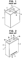
- FIG. 1 of the accompanying drawings illustrates such a conventional dielectric filter comprising a dielectric block A which is provided with two resonators B and has one end surface or a short-circuit end surface C provided with a region D having no short-circuit conductor between the resonators B as interstage coupling means of the resonators of the dielectric filter (Refer to Japanese Patent Kokai No. 3-293802).
- Japanese Patent Application No. 6-163189 Japanese Patent Kokai No. 8-8607
- a dielectric filter for a high frequency band as shown in FIG. 2 realized by providing a dielectric block 1 with a pair of through holes 2a and 2b extending in parallel with each other therethrough, providing internal conductors 3a and 3b on the inner surfaces of the respective through holes 2a and 2b to produce a pair of dielectric coaxial resonators, providing an external conductor 4 on a given area of the outer peripheral surface and providing a short-circuit conductor on one of the end surfaces of the dielectric block 1 to make it a short-circuit conductor end surface 5 for connecting the external conductor 4 and the internal conductor 3a and 3b, the other end surface.
- a slot 7 is formed by removing the external conductor 4 along a direction perpendicular to the through holes 2a and 2b in an area of the outer peripheral surface located close to the short-circuit conductor end surface 3 in order to couple and polarize the dielectric coaxial resonators at a same time in a simple manner.
- the slot is required to have a considerable width and hence a large surface area that occupies about 2/3 of the total area of the short-circuit end surface to ensure a sufficient coupling effect at the cost of a reduced Q value.
- the slot formed on the short-circuit end surface along a direction perpendicular to and between the resonators can reduce the mechanical strength of the dielectric filter (Refer to Japanese UM Kokai No. 62-61504).
- a shield case is applied thereto typically after directly connecting input/output terminals formed on the lower portion of the outer peripheral surface located opposite to the side of the coupling slot is connected directly with a printed circuit board.
- the inner wall of the shield case has to be separated from the coupling slot on the top side of the outer peripheral surface by at least 3mm because the coupling effect of the slot changes significantly when the inner wall of the shield case comes too close to or into contact with the coupling slot on the top side of the outer peripheral surface. This involves a problem that a dielectric filter for a high frequency band cannot reduce its height beyond a certain degree.
- the above object is achieved by providing a dielectric filter in which a plurality of through holes are provided to be extended between oppositely disposed end surfaces of a dielectric block in parallel with each other, each through hole has an inner peripheral surface provided with an internal conductor for forming a plurality of resonators, an external conductor is provided on a substantial portion of the outer peripheral surface of the dielectric block, one of the end surfaces is a short-circuit end surface provided with a short-circuiting conductor for connecting the external conductor on the outer peripheral surface and the internal conductors on the inner peripheral surfaces of the through holed, and the other end surface is an open-circuit end surface, wherein at least one region devoid of short-circuiting conductor is formed on the short-circuit end surface and extends in parallel with the direction connecting the resonators.
- the region devoid of short-circuiting conductor formed on the short-circuit end surface of the dielectric block may extend along at least an edge of the short-circuit end surface.
- the region devoid of short-circuiting conductor formed on the short-circuit end surface may comprise a slot extending along at least an edge of the short-circuit end surface.
- the region devoid of short-circuiting conductor extending along the direction connecting the resonators may have a width selected between a value equal to the distance separating the axes of any two adjacently located resonators and a value smaller than the width of the block.
- the dielectric coaxial resonators formed in the respective through hole are coupled for electric field at the open-circuit end surface and for magnetic field at the short-circuit end surface. Therefore, the magnetic coupling of the resonators are intensified because the magnetic field is made less apt to swerve to the external conductor side by the region devoid of short-circuit conductor formed along an edge of the short-circuit end surface running in parallel with the direction connecting the resonators. Thus, they are couple more intensely for magnetic field than for electric field so that any adjacently located resonators are coupled intensely for magnetic field to give rise to an interstage coupling.
- Such a region devoid of short-circuiting conductor may advantageously be formed by producing a transversal slit on an end surface of the dielectric block typically by means of a dicing saw and removing the short-circuit conductor in that region.
- the slit may be formed in the operation of producing a dielectric block by press machining. If such is the case, the short-circuit conductor surface is produced by applying a conductive material onto that surface except the slit.
- the region devoid of short-circuiting conductor may be produced by applying a conductive material to the entire surface and thereafter partly removing it to form a slit by means of a laser trimmer or sand blast.
- the non-conductive region may be formed by screen printing or patterning at the timing of forming a film of a short-circuit conductor.
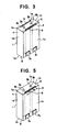
- FIGS. 3 and 4 illustrating an embodiment of dielectric filter according to the invention.
- FIGS. 3 and 4 there is shown a two-stage type dielectric filter for a high frequency band comprising a pair of dielectric coaxial resonators formed in a single dielectric block 1.
- the dielectric block 1 is a rectangular parallelpiped made of a ceramic dielectric material containing titanium and having an end surface 1a, another end surface 1b and four outer lateral side surfaces 1c, 1d, 1e and 1f.
- a pair of through holes 2a and 2b are bored through the dielectric block 1 in parallel with each other and extend between one end surface 1a and the other end surface 1b.
- Internal conductors 3a and 3b are formed respectively on the inner peripheral surfaces of the through holes 2a and 2b by applying a conductive material to produce a pair of dielectric coaxial resonators.
- An external conductor 4 is formed on the outer lateral side surfaces 1c, 1d, 1e and 1f and is used as a grounding conductor.
- a short-circuit conductor 5 is formed on the end surface 1a and electrically connected to the external conductor 4 on the outer lateral side surfaces 1c, 1d, 1e and 1f.
- the short-circuit conductor 5 electrically connects the internal conductors 3a and 3b of the dielectric coaxial resonators to the external conductor 4.
- the end surface 1a may well be referred to as short-circuit end surface.
- the other end surface 1b of the dielectric block 1 carries no conductor and therefore operates as an open-circuit end surface 6.
- Input/output conductors 7a and 7b are formed on the outer lateral side surface 1c and electrically insulated from the external conductor 4.
- the input/output conductor 7a is capacitively connecter to the internal conductor 3a via the dielectric block 1
- the input/output conductor 7b is capacitively connected to the internal conductor 3b also via the dielectric block 1.
- One of the input/output conductors 7a and 7b is connected to an input terminal of an electric circuit while the other input/ output conductor is connected to an output terminal of the circuit to complete the electric connection of the dielectric filter for a high frequency band.
- a pair of regions 8 and 9 devoid of short-circuit conductor or non-conductive regions are formed along the oppositely disposed respective edges of the short-circuit end surface 5, extending along the direction connecting the resonators as shown in FIGS. 3 and 4.
- the regions 8 and 9 devoid of short-circuit conductor may be formed by coating the end surface 1a with a short-circuit conductor and subsequently removing it to form the regions typically by means of a laser trimmer or sand blast.
- the regions 8 and 9 devoid of short-circuit conductor may be formed by producing a pair of transversal shallow slits typically by means of a dicing saw and removing the short-circuit conductor in that regions as shown in FIGS. 4B and 4C.
- the slits may be formed in the operation of producing a dielectric block by press machining. If such is the case, the short-circuit conductor surface is produced by applying a conductive material onto that surface except the slits, which then becomes regions 8 and 9 devoid of short-circuit conductor.
- the non-conductive regions may be formed by screen printing or patterning at the timing of forming an external conductor and a film of a short-circuit conductor.
- FIGS. 4A, 4B and 4C show dimensional values of the dielectric filter for a high frequency band thus constructed.
- FIG. 5 illustrates a modification of the embodiment of FIG.3, in which a single non-conductive region 8 is formed along one of the edges of the short-circuit end surface 5, extending along the direction connecting the resonators.
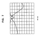
- FIGS. 6 through 9 are graphs illustrating an electric characteristic of such a dielectric filter having such a configuration as shown in FIG. 5 observed when different values were used for the width W1 of the region 8.
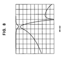
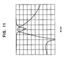
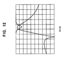
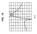
- FIGS. 10 through 13 show graphs illustrating the electric characteristic of the conventional dielectric filter as shown in FIG. 1 also observed when different values were used for the width W of the region D devoid of short-circuit conductor.
- the region devoid of short-circuit conductor of the dielectric filter according to the invention has a relatively small area of about 1/3 of the short-circuit end surface and the dielectric filter shows a satisfactory coupling effect
- the comparable region of the conventional dielectric filter of FIG. 1 has to be made as large as about 2/3 of the short-circuit end surface to achieve a similar coupling effect.
- the conventional dielectric filter such as shown in FIG. 1 is accompanied by a problem of regulating difficulty and a reduced Q value.
- the dielectric filter of the present invention shows an excellent controllability if compared with the conventional dielectric filter of FIG. 1 where a region devoid of short-circuit conductor is formed between the resonators.
- the present invention is applicable to a three-stage type dielectric filter comprising three dielectric coaxial resonators or a four- or higher stage type dielectric filter.
- the performance of a dielectric filter according to the invention (in terms of frequency bandwidth, attenuation pole generating frequency, etc.) can be controlled by regulating the position and the surface area of the region devoid of short-circuit conductor. Therefore, the region devoid of short-circuit conductor may be modified transversally (in the Y-direction) and/or longitudinally (in the X-direction) to substantially change its location and/or area in order to regulate the performance of the dielectric filter after forming the region.
- the dielectric filter according to the invention since a region devoid of short-circuit conductor is formed on the short-circuit end surface along a direction connecting the through holes to realize an interstage coupling, no coupling groove, slit nor spot facing has to be formed after producing a dielectric block for the filter so that such a dielectric filter can be manufactured efficiently in a well controlled manner with a desired coupling performance without reducing the Q value and a reduced mechanical strength.
- the present invention provide a remarkable technological advantage for manufacturing a dielectric filter for a high frequency band that operates stably and reliably.
Landscapes
- Physics & Mathematics (AREA)
- Electromagnetism (AREA)
- Control Of Motors That Do Not Use Commutators (AREA)
Applications Claiming Priority (3)
| Application Number | Priority Date | Filing Date | Title |
|---|---|---|---|
| JP7620796 | 1996-03-29 | ||
| JP7620796 | 1996-03-29 | ||
| JP76207/96 | 1996-03-29 |
Publications (3)
| Publication Number | Publication Date |
|---|---|
| EP0798803A2 true EP0798803A2 (fr) | 1997-10-01 |
| EP0798803A3 EP0798803A3 (fr) | 1998-07-15 |
| EP0798803B1 EP0798803B1 (fr) | 2003-04-23 |
Family
ID=13598730
Family Applications (1)
| Application Number | Title | Priority Date | Filing Date |
|---|---|---|---|
| EP97200900A Expired - Lifetime EP0798803B1 (fr) | 1996-03-29 | 1997-03-25 | Filtre diélectrique |
Country Status (3)
| Country | Link |
|---|---|
| US (1) | US5844454A (fr) |
| EP (1) | EP0798803B1 (fr) |
| DE (1) | DE69721113D1 (fr) |
Cited By (3)
| Publication number | Priority date | Publication date | Assignee | Title |
|---|---|---|---|---|
| DE19857358A1 (de) * | 1998-11-03 | 2000-05-18 | Samsung Electro Mech | Dielektrisches Filter |
| WO2000077883A1 (fr) * | 1999-06-15 | 2000-12-21 | Cts Corp. | Procede ablatif de formation de filtres rf de blocs de ceramique |
| US6559735B1 (en) | 2000-10-31 | 2003-05-06 | Cts Corporation | Duplexer filter with an alternative signal path |
Families Citing this family (4)
| Publication number | Priority date | Publication date | Assignee | Title |
|---|---|---|---|---|
| JP3123885B2 (ja) * | 1994-06-21 | 2001-01-15 | 日本特殊陶業株式会社 | 高周波用誘電体フィルタ |
| JP3577954B2 (ja) * | 1997-08-29 | 2004-10-20 | 株式会社村田製作所 | 誘電体フィルタ、デュプレクサ及び通信機装置 |
| CN111740193B (zh) * | 2020-06-23 | 2025-10-03 | 大富科技(安徽)股份有限公司 | 介质滤波器及通信基站 |
| CN113036325B (zh) | 2021-01-26 | 2022-08-12 | 嘉兴佳利电子有限公司 | 一种介质滤波器 |
Family Cites Families (9)
| Publication number | Priority date | Publication date | Assignee | Title |
|---|---|---|---|---|
| US4464640A (en) * | 1981-10-02 | 1984-08-07 | Murata Manufacturing Co., Ltd. | Distribution constant type filter |
| JPS58204601A (ja) * | 1982-05-24 | 1983-11-29 | Murata Mfg Co Ltd | 分布定数形フイルタの帯域巾調整方法 |
| JPS6152003A (ja) * | 1984-08-21 | 1986-03-14 | Murata Mfg Co Ltd | 誘電体フイルタ |
| JPS6261504A (ja) * | 1985-09-12 | 1987-03-18 | 井関農機株式会社 | トラクタにおける油圧制御装置 |
| JPH0389602A (ja) * | 1989-08-31 | 1991-04-15 | Taiyo Yuden Co Ltd | 誘電体フィルタの通過帯域調整方法 |
| JPH03293802A (ja) * | 1990-04-11 | 1991-12-25 | Murata Mfg Co Ltd | 誘電体フィルタ |
| EP0556573B1 (fr) * | 1992-01-22 | 1998-09-23 | Murata Manufacturing Co., Ltd. | Résonateur diélectrique et procédé de réglage de sa caractéristique |
| JP3293200B2 (ja) * | 1992-04-03 | 2002-06-17 | 株式会社村田製作所 | 誘電体共振器 |
| JP3123885B2 (ja) * | 1994-06-21 | 2001-01-15 | 日本特殊陶業株式会社 | 高周波用誘電体フィルタ |
-
1997
- 1997-03-24 US US08/823,206 patent/US5844454A/en not_active Expired - Fee Related
- 1997-03-25 EP EP97200900A patent/EP0798803B1/fr not_active Expired - Lifetime
- 1997-03-25 DE DE69721113T patent/DE69721113D1/de not_active Expired - Lifetime
Cited By (6)
| Publication number | Priority date | Publication date | Assignee | Title |
|---|---|---|---|---|
| DE19857358A1 (de) * | 1998-11-03 | 2000-05-18 | Samsung Electro Mech | Dielektrisches Filter |
| US6169464B1 (en) | 1998-11-03 | 2001-01-02 | Samsung Electro-Mechanics Co., Ltd. | Dielectric filter |
| WO2000077883A1 (fr) * | 1999-06-15 | 2000-12-21 | Cts Corp. | Procede ablatif de formation de filtres rf de blocs de ceramique |
| US6462629B1 (en) | 1999-06-15 | 2002-10-08 | Cts Corporation | Ablative RF ceramic block filters |
| US6834429B2 (en) | 1999-06-15 | 2004-12-28 | Cts Corporation | Ablative method for forming RF ceramic block filters |
| US6559735B1 (en) | 2000-10-31 | 2003-05-06 | Cts Corporation | Duplexer filter with an alternative signal path |
Also Published As
| Publication number | Publication date |
|---|---|
| DE69721113D1 (de) | 2003-05-28 |
| EP0798803B1 (fr) | 2003-04-23 |
| US5844454A (en) | 1998-12-01 |
| EP0798803A3 (fr) | 1998-07-15 |
Similar Documents
| Publication | Publication Date | Title |
|---|---|---|
| US4996506A (en) | Band elimination filter and dielectric resonator therefor | |
| EP1947731A1 (fr) | Filtre diélectrique, duplexeur diélectrique, et appareil de communication | |
| US5929726A (en) | Dielectric filter device | |
| EP0757401A2 (fr) | Filtre diélectrique | |
| US5844454A (en) | Dielectric filter with non-conductive edge | |
| US5949308A (en) | Dielectric filter and method of regulating its frequency bandwidth via at least one insulation gap | |
| JP3123885B2 (ja) | 高周波用誘電体フィルタ | |
| US5859575A (en) | Dielectric filter | |
| EP0568370B1 (fr) | Dispositif à filtrage diélectrique | |
| JPH03108801A (ja) | 誘電体フィルタ | |
| JP2661007B2 (ja) | 誘電体フィルタとその通過帯域幅調整方法 | |
| JPH06216605A (ja) | ストリップラインフィルタ | |
| EP0837518B1 (fr) | Filtre diélectrique | |
| US6034579A (en) | Dielectric filter of the band elimination type | |
| KR100213374B1 (ko) | 소형 유전체 필터 | |
| JP2661006B2 (ja) | 誘電体フィルタ | |
| JPH09321503A (ja) | 誘電体フィルタ | |
| JPH0818306A (ja) | 誘電体フィルタ | |
| JP3614710B2 (ja) | 誘電体フィルタ | |
| JP2661004B2 (ja) | 誘電体フィルタ | |
| JPH07221521A (ja) | 誘電体共振器およびこれを使用する誘電体フィルタ | |
| JP3469476B2 (ja) | 誘電体フィルタ | |
| KR960012467B1 (ko) | 유전체를 이용한 고주파 필터의 결합구조 | |
| JPH0685503A (ja) | 誘電体フィルタ | |
| JPH06164206A (ja) | 誘電体フィルタおよび誘電体フィルタと回路基板との組合わせ構造 |
Legal Events
| Date | Code | Title | Description |
|---|---|---|---|
| PUAI | Public reference made under article 153(3) epc to a published international application that has entered the european phase |
Free format text: ORIGINAL CODE: 0009012 |
|
| 17P | Request for examination filed |
Effective date: 19970325 |
|
| AK | Designated contracting states |
Kind code of ref document: A2 Designated state(s): DE FR GB |
|
| PUAL | Search report despatched |
Free format text: ORIGINAL CODE: 0009013 |
|
| AK | Designated contracting states |
Kind code of ref document: A3 Designated state(s): DE FR GB |
|
| 17Q | First examination report despatched |
Effective date: 20010718 |
|
| GRAH | Despatch of communication of intention to grant a patent |
Free format text: ORIGINAL CODE: EPIDOS IGRA |
|
| GRAH | Despatch of communication of intention to grant a patent |
Free format text: ORIGINAL CODE: EPIDOS IGRA |
|
| GRAA | (expected) grant |
Free format text: ORIGINAL CODE: 0009210 |
|
| AK | Designated contracting states |
Designated state(s): DE FR GB |
|
| PG25 | Lapsed in a contracting state [announced via postgrant information from national office to epo] |
Ref country code: FR Free format text: LAPSE BECAUSE OF FAILURE TO SUBMIT A TRANSLATION OF THE DESCRIPTION OR TO PAY THE FEE WITHIN THE PRESCRIBED TIME-LIMIT Effective date: 20030423 |
|
| REG | Reference to a national code |
Ref country code: GB Ref legal event code: FG4D |
|
| REF | Corresponds to: |
Ref document number: 69721113 Country of ref document: DE Date of ref document: 20030528 Kind code of ref document: P |
|
| PG25 | Lapsed in a contracting state [announced via postgrant information from national office to epo] |
Ref country code: DE Free format text: LAPSE BECAUSE OF FAILURE TO SUBMIT A TRANSLATION OF THE DESCRIPTION OR TO PAY THE FEE WITHIN THE PRESCRIBED TIME-LIMIT Effective date: 20030724 |
|
| PLBE | No opposition filed within time limit |
Free format text: ORIGINAL CODE: 0009261 |
|
| STAA | Information on the status of an ep patent application or granted ep patent |
Free format text: STATUS: NO OPPOSITION FILED WITHIN TIME LIMIT |
|
| 26N | No opposition filed |
Effective date: 20040126 |
|
| EN | Fr: translation not filed | ||
| PGFP | Annual fee paid to national office [announced via postgrant information from national office to epo] |
Ref country code: GB Payment date: 20080326 Year of fee payment: 12 |
|
| GBPC | Gb: european patent ceased through non-payment of renewal fee |
Effective date: 20090325 |
|
| PG25 | Lapsed in a contracting state [announced via postgrant information from national office to epo] |
Ref country code: GB Free format text: LAPSE BECAUSE OF NON-PAYMENT OF DUE FEES Effective date: 20090325 |