EP0798955A1 - Verfahren und Vorrichtung zum Abziehen von Chips - Google Patents
Verfahren und Vorrichtung zum Abziehen von Chips Download PDFInfo
- Publication number
- EP0798955A1 EP0798955A1 EP97302085A EP97302085A EP0798955A1 EP 0798955 A1 EP0798955 A1 EP 0798955A1 EP 97302085 A EP97302085 A EP 97302085A EP 97302085 A EP97302085 A EP 97302085A EP 0798955 A1 EP0798955 A1 EP 0798955A1
- Authority
- EP
- European Patent Office
- Prior art keywords
- chips
- protrusions
- sheet
- peeling
- wafer
- Prior art date
- Legal status (The legal status is an assumption and is not a legal conclusion. Google has not performed a legal analysis and makes no representation as to the accuracy of the status listed.)
- Granted
Links
Images


Classifications
-
- H—ELECTRICITY
- H10—SEMICONDUCTOR DEVICES; ELECTRIC SOLID-STATE DEVICES NOT OTHERWISE PROVIDED FOR
- H10P—GENERIC PROCESSES OR APPARATUS FOR THE MANUFACTURE OR TREATMENT OF DEVICES COVERED BY CLASS H10
- H10P72/00—Handling or holding of wafers, substrates or devices during manufacture or treatment thereof
- H10P72/04—Apparatus for manufacture or treatment
- H10P72/0442—Apparatus for placing on an insulating substrate, e.g. tape
-
- H—ELECTRICITY
- H05—ELECTRIC TECHNIQUES NOT OTHERWISE PROVIDED FOR
- H05K—PRINTED CIRCUITS; CASINGS OR CONSTRUCTIONAL DETAILS OF ELECTRIC APPARATUS; MANUFACTURE OF ASSEMBLAGES OF ELECTRICAL COMPONENTS
- H05K13/00—Apparatus or processes specially adapted for manufacturing or adjusting assemblages of electric components
- H05K13/04—Mounting of components, e.g. of leadless components
- H05K13/0417—Feeding with belts or tapes
-
- H—ELECTRICITY
- H10—SEMICONDUCTOR DEVICES; ELECTRIC SOLID-STATE DEVICES NOT OTHERWISE PROVIDED FOR
- H10P—GENERIC PROCESSES OR APPARATUS FOR THE MANUFACTURE OR TREATMENT OF DEVICES COVERED BY CLASS H10
- H10P72/00—Handling or holding of wafers, substrates or devices during manufacture or treatment thereof
- H10P72/70—Handling or holding of wafers, substrates or devices during manufacture or treatment thereof for supporting or gripping
- H10P72/74—Handling or holding of wafers, substrates or devices during manufacture or treatment thereof for supporting or gripping using temporarily an auxiliary support
- H10P72/7412—Handling or holding of wafers, substrates or devices during manufacture or treatment thereof for supporting or gripping using temporarily an auxiliary support the auxiliary support including means facilitating the separation of a device or wafer from the auxiliary support
- H10P72/7414—Handling or holding of wafers, substrates or devices during manufacture or treatment thereof for supporting or gripping using temporarily an auxiliary support the auxiliary support including means facilitating the separation of a device or wafer from the auxiliary support the auxiliary support including means facilitating the selective separation of some of a plurality of devices from the auxiliary support
-
- Y—GENERAL TAGGING OF NEW TECHNOLOGICAL DEVELOPMENTS; GENERAL TAGGING OF CROSS-SECTIONAL TECHNOLOGIES SPANNING OVER SEVERAL SECTIONS OF THE IPC; TECHNICAL SUBJECTS COVERED BY FORMER USPC CROSS-REFERENCE ART COLLECTIONS [XRACs] AND DIGESTS
- Y10—TECHNICAL SUBJECTS COVERED BY FORMER USPC
- Y10T—TECHNICAL SUBJECTS COVERED BY FORMER US CLASSIFICATION
- Y10T225/00—Severing by tearing or breaking
- Y10T225/10—Methods
- Y10T225/12—With preliminary weakening
-
- Y—GENERAL TAGGING OF NEW TECHNOLOGICAL DEVELOPMENTS; GENERAL TAGGING OF CROSS-SECTIONAL TECHNOLOGIES SPANNING OVER SEVERAL SECTIONS OF THE IPC; TECHNICAL SUBJECTS COVERED BY FORMER USPC CROSS-REFERENCE ART COLLECTIONS [XRACs] AND DIGESTS
- Y10—TECHNICAL SUBJECTS COVERED BY FORMER USPC
- Y10T—TECHNICAL SUBJECTS COVERED BY FORMER US CLASSIFICATION
- Y10T29/00—Metal working
- Y10T29/49—Method of mechanical manufacture
- Y10T29/49789—Obtaining plural product pieces from unitary workpiece
- Y10T29/4979—Breaking through weakened portion
Definitions
- the present invention relates to a method of and an apparatus for peeling chips fabricated on a wafer of silicon or the like off a sheet attached to the reverse side of the wafer in a process of manufacturing ICs or the like.
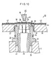
- FIG. 10 of the accompanying drawings shows a conventional chip peeling apparatus 10.
- the conventional chip peeling apparatus 10 includes a base 12 having a hole 16 defined therein which is connected to a first vacuum source (not shown).
- a tubular member 18 has an end fitted in an upper open end of the hole 16 and a flange 20 projecting radially outwardly from an outer circumferential surface thereof.
- the flange 20 is fixedly mounted on the end of the base 12 which defines the upper open end of the hole 16, thereby supporting the tubular member 18 on the base 12.
- a cylindrical member 22 is inserted in the hole 16 and has an outer wall surface and a distal end spaced from an inner wall surface of the tubular member 18 which defines a hole 24 therein.
- a pin 26 is inserted in the cylindrical member 22 for axial sliding movement in the cylindrical member 22, and supports a plurality of needles 28 mounted upwardly on a distal end of the pin 26.
- a suction nozzle 30 is fitted in a distal end of the tubular member 18 and fixed to the tubular member 18 by a cover 32.
- the suction nozzle 30 has a plurality of holes 34 defined therein for insertion of the needles 28.
- a seat 36 is positioned in upwardly spaced relation to the base 12, and the suction nozzle 30 has a distal end projecting upwardly slightly from a hole 37 that is defined in the seat 36.
- a suction head 38 is disposed upwardly of the suction nozzle 30 for movement toward and away from the suction nozzle 30.
- the suction head 38 has an axial hole 40 defined therein which is connected to a section vacuum source (not shown).
- a process of peeling chips 42 such as of ICs or the like fabricated on a wafer off a sheet 44 using the chip peeling apparatus 10 will be described below.
- the sheet 44 to which the chips 42 are attached is moved to a position above the seat 36 and brought into held against an upper portion of the suction nozzle 30, the sheet 44 is curved upwardly.
- the first vacuum source (not shown) is actuated to attract the sheet 44 to the suction nozzle 30.
- the pin 26 is lifted to cause the needles 28 to pierce and project through the sheet 44, and ascend with the chip 42 placed on the tips of the needles 28, as shown in FIG. 11 of the accompanying drawings.
- the chip 42 is peeled off the sheet 44.
- the suction head 38 is moved toward the suction nozzle 30 and brought into abutment against the chip 42.
- the second vacuum source (not shown) is actuated to attract the chip 42 off the sheet 44 to the suction head 38.
- the chip 42 will then be transferred to another location.
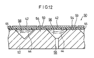
- FIG. 11 of the accompanying drawings shows another conventional chip peeling apparatus 50.
- the conventional chip peeling apparatus 50 includes a peeling base 52 having a plurality of protrusions 54 with flat tops, the protrusions 54 having heaters (not shown).
- the peeling base 52 has grooves 56 each defined between adjacent ones or the protrusions 54 and communicating with a hole 58 defined in the peeling base 52 which is connected to a vacuum source (not shown).
- a suction head (not shown) is positioned above one of the grooves 56 for movement toward and away from the peeling base 52.
- a sheet 44 with a plurality of chips 42 and streets 59 remaining as cut fragments in gaps between the chips 42 is moved toward a position above the peeling base 52 with the chips 42 above the grooves 56.
- the protrusions 54 have been heated by the heater to apply heat to the sheet 44 for thereby making the sheet 44 stretchable.
- the vacuum source is actuated to evacuate the grooves 56, whereupon the sheet 44 is stretched and curved in the direction in which the vacuum is developed, as indicated by the two-dot-and-dash lines.
- the chips 42 have their peripheral edges supported on the flat tops of the protrusions 54, and the sheet 44 is peeled off central regions of the chips 42.
- the suction head (not shown) is moved toward a desired one of the chips 42. Because of an attracting action of the suction head, the sheet 44 is peeled off the peripheral edges of the chip 42, which is attracted to and held by the suction head. The chip 42 will then be transferred to another location.
- the former chip peeling apparatus 10 is disadvantageous in that the tips of the needles 28 tend to damage the surface of the chip 42.
- the sheet 44 itself may also be stretched and lifted. At this time, the needles 28 may not pierce the sheet 44, an hence may not form holes in the sheet 44, with the result the chip 44 may not be separated from the sheet 44.
- the latter chip peeling apparatus 50 is also problematic in that when the sheet 44 is attracted, the chip 42 itself may be curved, and when the sheet 44 is peeled off, the chip 42 may jump off, resulting in a positional deviation which may prevent the suction head from attract the chip 42. As a result, when the chip 42 is to be transferred to and placed in a next process, the chip 42 cannot be positioned with accuracy. When the chip 42 is curved, it cannot be prevented from being unduly curved to an unnecessary extent, and hence may be cracked or broken. If the chip 42 is broken, it is liable to damage the sheet 44, eliminating the vacuum thereby to fail to peel other normal chips 42 off the sheet 44. Furthermore, when a chip 42 is to be peeled off by the suction head, a street 59 which lies at the same height as the chip 42 may also be peeled off the sheet 44, and attracted and transferred together with the chip 42 by the suction head.
- a major object of the present invention is to provide a method of and an apparatus for peeling chips, which have been attached to a sheet and fed therewith, off the sheet without damage to the chips while allowing the chips to suffer undesirable positional deviations after the chips have been peeled off.
- Another object of the present invention is to provide a method of and an apparatus for peeling chips, which have been attached to a sheet and fed therewith, off the sheet without damage to the sheet while allowing other chips to be peeled reliably off the sheet.
- Still another object of the present invention is to provide a method of and an apparatus for peeling chips off a sheet without the possibility of peeling off streets attached to the sheet between the chips.
- Yet still another object of the present invention is to provide a method of and an apparatus for peeling chips, which have been attached to a sheet and fed therewith, off the sheet efficiently within a short period of time.
- the invention is set out in claims 1 and 3.
- the peeled-off chips are attracted, e.g. by vacuum, away from the sheet, for carrying them away.
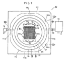
- FIGS. 1 and 2 show a chip peeling apparatus 60 according to an embodiment of the present invention.
- the chip peeling apparatus 60 includes a substantially square base 62 having a pair of pins 64a, 64b vertically mounted on an upper surface thereof. As shown in FIG. 2, the base 62 has a chamber 66 defined therein and pair of horizontal passages 68a, 68b defined therein which are held in communication with the chamber 66.
- the passage 68a is connected through a coupling 70 to a vacuum pump 72, and the passage 68b is connected to a bushing 74, to which the coupling of another chip peeling apparatus can be connected. Therefore, a plurality of chip peeling apparatus 60 may be connected in series with each other and coupled to the single vacuum pump 72.
- the base 62 also has a large-diameter upwardly open circular hole 78 defined therein which communicates with the chamber 66 with a horizontal step 76 extending therebetween.
- the step 76 has a circular groove 80 defined in its upper surface in surrounding relation to the chamber 66, with an annular O-ring 82 fitted in the groove 80.
- a circular seat 84 is fitted in the hole 78 and fastened to the base 62 by a screw 86.
- the seat 84 has a upwardly open circular recess 88 defined therein partly by a bottom which has a central hole 90 communicating with the chamber 66.
- the bottom which defines the circular recess 88 has a plurality of concentric annular ridges 91 disposed on its upper surface.
- a circular support base 92 is fitted in the recess 88 and supported on the annular ridges 91.
- the support base 92 is fastened to the seat 84 by a screw 93.
- the support base 92 also has a circular step 95 disposed on its upper surface and extending in the vicinity of an outer circumferential edge thereof, with a flat surface 97 lying radially inwardly of the step 95.
- the support base 92 further includes a substantially central hole 94 defined therein, with a peeling base 98 fitted in the hole 94.
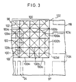
- the peeling base 98 will be described in detail below. As shown in FIGS. 3 and 4, the peeling base 98 has a plurality of closely positioned upward protrusions 100 each in the form of a quadrangular pyramid on its upper surface.
- the protrusions 100 include first protrusions 100a having a height h 1 and second protrusions 100b having a height h 2 which is smaller than the height h 1 .
- the difference t 1 between the heights h 1 , h 2 is equal to or smaller than a sheet thickness t 2 described later on.
- the first protrusions 100a are positioned so as to be aligned with respective corners 103a ⁇ 103d of chips 102 (described later on), and the second protrusions 100b are positioned in other regions. For example, if chips 102 are of a substantially square or rectangular shape, then the first protrusions 100a are positioned so as to abut against the four corners 103a ⁇ 103d of the chips 102.
- the peeling base 98 has a plurality of holes 106 defined vertically therein which communicate with grooves 104 that are defined between certain protrusions 100 and protrusions 100 adjacent thereto.
- the holes 106 communicate with the hole 90 defined in the seat 84. Therefore, the grooves 104 communicate with the vacuum pump 72 through the hole 90, the chamber 66, the passage 68a, and the coupling 70.
- Each of the holes 106 is positioned in the vicinity of the center of one of the chips 102.
- a holder plate 107 and a suction head 108 are disposed above the peeling base 98 for movement toward and away from the peeling base 98 by an actuator (not shown).
- the holder plate 107 is made of an electrically conductive material, and can be moved to a position that is spaced from the chips 102 by a distance equal to or smaller than the thickness t 3 of the chips 102.
- the suction head 108 has an axial hole 109 defined therein which communicates with a vacuum source (not shown).
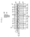
- a wafer retainer plate 110 for being mounted on the chip peeling apparatus 60 will be described below.
- the wafer retainer plate 110 is of a substantially circular shape and has a plurality of linear edges 111a, 111b, 111c, 111d in respective 90°-spaced positions.
- the wafer retainer plate 110 has recesses 112a, 112b defined in outer circumferential edges thereof one on each side of the linear edge 111b.
- the wafer retainer plate 110 has a step 113 defined in a lower surface thereof for engagement with the step 95 of the support base 92.
- the wafer retainer plate 110 has a substantially rectangular hole 114 defined centrally therein by walls having a plurality of inwardly projecting teeth 116.
- an ultraviolet radiation absorbing, flexible sheet (hereinafter referred to as a "UV sheet” ) 126 having a thickness t 2 is attached to the lower surface of the wafer retainer plate 110.
- a substantially square wafer 118 of silicon or the like is disposed in the hole 114 and held against an upper surface of the UV sheet 126.
- the wafer 118 has a plurality of square chips 102 and a plurality of elongate rectangular streets 122 remaining as cut fragments in gaps between the chips 102.
- the wafer 118 also has a tab 124 on its outer peripheral edges in surrounding relation to the chips 102.
- the streets 122 and the tab 124 are unwanted parts that are produced in a process of fabricating the chips 102, and will be discarded after the chips 102 are fabricated.
- the wafer retainer plate 110 which is holding the wafer 118 is placed on the chip peeling apparatus 60.
- the wafer 118 is positioned with respect to the chip peeling apparatus 60 by bringing the walls of the recesses 112a, 112b into engagement with the pins 64a, 64b.
- the first protrusions 110a have their tops held in abutment against the UV sheet 126 on the reverse side of the chips 102 in the vicinity of the four corners 103a ⁇ 103d of the chips 102, thus supporting the chips 102.
- FIG. 1 the wafer retainer plate 110 which is holding the wafer 118 is placed on the chip peeling apparatus 60.
- the wafer 118 is positioned with respect to the chip peeling apparatus 60 by bringing the walls of the recesses 112a, 112b into engagement with the pins 64a, 64b.
- the first protrusions 110a have their tops held in abutment against the UV sheet 126 on the reverse side of the chips 102 in the vicinity of the
- the tops of the second protrusions 100b are spaced from the UV sheet 126 by the distance t 1 which is equal to or smaller than the thickness t 2 of the UV sheet 126.
- the streets 122 are positioned between first protrusions 100a and first protrusions 100a adjacent thereto, and are not supported by the first protrusions 100a or the second protrusions 100b.
- the tab 124 is positioned over the flat surface 97, and in intimate contact therewith through the UV sheet 126.
- the vacuum pump 72 When the vacuum pump 72 is actuated, air in the grooves 104 is discharged through the holes 106, the hole 90, and the passage 68a, lowering the air pressure in the grooves 104.
- the UV sheet 126 As shown in FIG. 6, the UV sheet 126 is stretched into the grooves 104 under a vacuum, lowering the streets 122 which are not supported by the protrusions 100. The UV sheet 126 is now peeled off the edges of the chips 102. Since the streets 122 descend with the UV sheet 126 at this time, the streets 122 are not peeled off the UV sheet 126.
- the central areas of the chips 102 are curved downwardly, as shown in FIG. 7.
- the central areas of the chips 102 abut against and are supported by the tops of the second protrusions 100b, preventing the chips 102 from being curved further downwardly. Since the curved chips 102 are subjected to forces tending to recover them, the chips 102 gradually restore their original shape, allowing the UV sheet 126 to be gradually peeled off the chips 102.
- the UV sheet 126 On the tops of the second protrusions 100b, the UV sheet 126 remains attached to the chips 102 until the chips 102 return to their original flat shape, when the UV sheet 126 is peeled off the chips 102 on the tops of the second protrusions 100b, as shown in FIG. 8.
- the holder plate 107 is effective in preventing the chips 102 from unduly jumping off, and hence preventing them from being positionally deviated. Inasmuch as the holder plate 107 is made of an electrically conductive material, the chips 102 are not attracted to the holder plate 107 because of electrostatic charges which are developed when the UV sheet 126 is peeled off the chips 102.
- the UV sheet 126 is prevented from being unduly stretched by the abutment against the second protrusions 100b, the UV sheet 126 is protected against damage. Since the UV sheet 126 is not damaged, the vacuum created in the grooves 104 is securely maintained, avoiding the possibility of an undesirable peel-off failure of the chips 102. If adjacent chips 102 are peeled off the UV sheet 126 at different times, then the UV sheet 126 is subject to a horizontal force tending to move the UV sheet 126 horizontally. However, since the UV sheet 126 is held against the tops of the first and second protrusions 100a, 100b, the UV sheet 126 is prevented from being moved horizontally even under such a horizontal force, thus preventing the chips 102 from being positionally deviated.
- the holder plate 107 is displaced away from the chips 102, and the suction head 108 is lowered into abutment against one of the chips 102.
- the vacuum source connected to the suction head 108 is actuated to attract the chip 102 to the suction head 108.
- the suction head 108 is then elevated. Since the UV sheet 126 is attached to the chip 102 through a small area on the tops of the corresponding first protrusions 100a, the chip 102 is peeled off the UV sheet 126 with a small force, and held by the suction head 108, as shown in FIG. 9.
- the suction head 108 then carries the chip 102 to a next process.
- the chips 102 will successively be peeled off the UV sheet 126 in the manner described above. Since the streets 122 are not peeled off the UV sheet 126, the streets 122 will not be delivered to the next process.
- the tab 126 is held in intimated contact with the upper surface of the flat surface 97 through the UV sheet 126, as described above. Therefore, the tab 126 will not be peeled off the UV sheet 126.
- a peeling test was conducted on the chips 102 using the chip peeling method and the chip peeling apparatus 60 described above. Details and results of the peeling test will be described below with respect to experimental and comparative examples.
- the tops of adjacent ones of the protrusions 100 of a peeling base 98a were spaced 2.63 mm in an X-axis direction and 3.12 mm in a Y-axis direction.
- Four first protrusions 100a and five second protrusions 100b were closely positioned in a square pattern as shown in FIG. 3. Specifically, the first protrusions 100a were positioned in alignment with the four corners 103a ⁇ 103d of a chip 102, and the second protrusions 100b were positioned in other regions.
- a water 118 was placed on the chip peeling apparatus 60, and the vacuum pump 72 was actuated to peel the UV sheet 126.
- the time required for peeling the UV sheet 126, the positional deviation which the chip 102 suffered when the UV sheet 126 was peeled, the frequency with which the chip 102 was skewed when the UV sheet 126 was peeled, the frequency with which the chip 102 jumped when the UV sheet 126 was peeled, and the frequency of peeling failures between the UV sheet 126 and the chip 102 were measured.
- Peeling bases 98b ⁇ 98d with protrusions 100 of equal height were produced.
- the tops of adjacent ones of the protrusions 100 were spaced 3 mm in the X-axis direction and 3 mm in the Y-axis direction.
- the tops of adjacent ones of the protrusions 100 were spaced 2.5 mm in the X-axis direction and 2.5 mm in the Y-axis direction.
- the tops of adjacent ones of the protrusions 100 were spaced 1.94 mm in the X-axis direction and 2.34 mm in the Y-axis direction.
- the number of protrusions 100 for supporting one chip 102 was 9 on the peeling base 98b, 16 on the peeling base 98c, and 16 on the peeling base 98d.
- the time required for peeling the UV sheet 126, the positional deviation which the chip 102 suffered when the UV sheet 126 was peeled, the frequency with which the chip 102 was skewed when the UV sheet 126 was peeled, the frequency with which the chip 102 jumped when the UV sheet 126 was peeled, and the frequency of peeling failures between the UV sheet 126 and the chip 102 were also measured with respect to these peeling bases 98b, 98c, 98d.
- the chip peeling apparatus 60 according to the present invention had a short peeling time, suffered no positional deviation of the chip 102, and did not cause the chip 102 to be skewed, jump, and suffer a peeling failure.
- the peeling time was long, the chip 102 suffered a positional deviation, was skewed, and jumped though no peeling failure occurred.
- the peeling base 98d the chip 102 suffered no positional deviation and did not jump, but the peeling time was quite long and the frequency of peeling failures was high.
- the chips are prevented from being damaged by needles which would otherwise be employed in the conventional chip peeling apparatus.
- the chips are curved, they are supported by the second protrusions and hence prevented being further curved. Therefore, the chips are prevented from being cracked or broken, and the sheet is protected against damage, preventing peeling failures which would otherwise take place due to the elimination of the vacuum needed to peel the chips off the sheet. Since forces tending to recover the chips are small, the chips do not suffer a possibility of positional deviations. Even if the chips are subject to large restoring forces, they are prevented from jumping off by the holder plate, and hence from being positionally deviated. Inasmuch as the time required to peel off the chips can be shortened, the chips can be peeled off the sheet with improved efficiency.
Landscapes
- Engineering & Computer Science (AREA)
- Manufacturing & Machinery (AREA)
- Microelectronics & Electronic Packaging (AREA)
- Container, Conveyance, Adherence, Positioning, Of Wafer (AREA)
- Die Bonding (AREA)
Applications Claiming Priority (3)
| Application Number | Priority Date | Filing Date | Title |
|---|---|---|---|
| JP77407/96 | 1996-03-29 | ||
| JP7740796 | 1996-03-29 | ||
| JP07740796A JP3441879B2 (ja) | 1996-03-29 | 1996-03-29 | チップ剥離装置 |
Publications (2)
| Publication Number | Publication Date |
|---|---|
| EP0798955A1 true EP0798955A1 (de) | 1997-10-01 |
| EP0798955B1 EP0798955B1 (de) | 1999-06-23 |
Family
ID=13633067
Family Applications (1)
| Application Number | Title | Priority Date | Filing Date |
|---|---|---|---|
| EP97302085A Expired - Lifetime EP0798955B1 (de) | 1996-03-29 | 1997-03-26 | Verfahren und Vorrichtung zum Abziehen von Chips |
Country Status (4)
| Country | Link |
|---|---|
| US (2) | US6106222A (de) |
| EP (1) | EP0798955B1 (de) |
| JP (1) | JP3441879B2 (de) |
| DE (1) | DE69700286T2 (de) |
Cited By (3)
| Publication number | Priority date | Publication date | Assignee | Title |
|---|---|---|---|---|
| DE19752582A1 (de) * | 1997-11-27 | 1999-06-10 | Inst Mikrotechnik Mainz Gmbh | Ablösevorrichtung für Mikrobauteile |
| DE10151441A1 (de) * | 2001-10-18 | 2003-05-15 | Infineon Technologies Ag | Anordnung und Verfahren zur Aufnahme und zum Bearbeiten eines dünnen Wafers |
| DE102006022277A1 (de) * | 2006-05-11 | 2007-11-15 | Deutsche Post Ag | Sauggreifer |
Families Citing this family (16)
| Publication number | Priority date | Publication date | Assignee | Title |
|---|---|---|---|---|
| JP2990197B1 (ja) * | 1999-01-20 | 1999-12-13 | 熊本日本電気株式会社 | 半導体チップのピックアップ装置 |
| JP2001196328A (ja) * | 2000-01-12 | 2001-07-19 | Disco Abrasive Syst Ltd | Csp基板の分割方法 |
| US20110005667A1 (en) * | 2002-05-10 | 2011-01-13 | Delphon Industries LLC | Multiple segment vacuum release handling device |
| US7780005B2 (en) * | 2002-05-10 | 2010-08-24 | Delphon Industries LLC | Multiple segment vacuum release handling device |
| US20030209847A1 (en) * | 2002-05-10 | 2003-11-13 | Allison Claudia Leigh | Handling device comprising multiple immobilization segments |
| AU2003902270A0 (en) * | 2003-05-09 | 2003-05-29 | Origin Energy Solar Pty Ltd | Separating and assembling semiconductor strips |
| JP4405211B2 (ja) * | 2003-09-08 | 2010-01-27 | パナソニック株式会社 | 半導体チップの剥離装置、剥離方法、及び半導体チップの供給装置 |
| KR100817068B1 (ko) * | 2006-10-24 | 2008-03-27 | 삼성전자주식회사 | 박형의 반도체 칩 픽업 장치 및 방법 |
| JP4693805B2 (ja) * | 2007-03-16 | 2011-06-01 | 株式会社東芝 | 半導体装置の製造装置及び製造方法 |
| JP5318557B2 (ja) * | 2008-12-24 | 2013-10-16 | 信越ポリマー株式会社 | 保持治具 |
| JP2013102126A (ja) * | 2011-10-14 | 2013-05-23 | Fuji Electric Co Ltd | 半導体装置の製造方法および半導体装置の製造装置 |
| JP2013191781A (ja) * | 2012-03-14 | 2013-09-26 | Fuji Electric Co Ltd | 半導体製造装置および半導体製造装置の制御方法 |
| US20150247879A1 (en) | 2014-03-03 | 2015-09-03 | Infineon Technologies Ag | Acceleration sensor |
| US9196520B1 (en) * | 2014-08-01 | 2015-11-24 | Freescale Semiconductor, Inc. | Tape release systems and methods for semiconductor dies |
| JP2018056159A (ja) * | 2016-09-26 | 2018-04-05 | セイコーエプソン株式会社 | 粘着テープ剥離治具、半導体チップの製造装置、memsデバイスの製造装置、液体噴射ヘッドの製造装置、および、粘着テープ剥離方法 |
| TWI880741B (zh) * | 2024-05-14 | 2025-04-11 | 矽品精密工業股份有限公司 | 分離裝置 |
Citations (2)
| Publication number | Priority date | Publication date | Assignee | Title |
|---|---|---|---|---|
| EP0431637A1 (de) * | 1989-12-08 | 1991-06-12 | Sumitomo Electric Industries, Ltd. | Aufnahmeverfahren und -apparat für einen chipähnlichen Teil |
| US5351872A (en) * | 1992-06-24 | 1994-10-04 | Kabushiki Kaisha Toshiba | Die bonding apparatus |
Family Cites Families (10)
| Publication number | Priority date | Publication date | Assignee | Title |
|---|---|---|---|---|
| US3988196A (en) * | 1967-10-09 | 1976-10-26 | Western Electric Company, Inc. | Apparatus for transferring an oriented array of articles |
| US3707760A (en) * | 1971-05-19 | 1973-01-02 | Sieburg Ind Inc | Method and device for article working such as fracturing of semiconductor slices and separating semiconductor chips |
| US3790051A (en) * | 1971-09-07 | 1974-02-05 | Radiant Energy Systems | Semiconductor wafer fracturing technique employing a pressure controlled roller |
| US3747282A (en) * | 1971-11-29 | 1973-07-24 | E Katzke | Apparatus for polishing wafers |
| US4778326A (en) * | 1983-05-24 | 1988-10-18 | Vichem Corporation | Method and means for handling semiconductor and similar electronic devices |
| US4556362A (en) * | 1983-12-21 | 1985-12-03 | At&T Technologies, Inc. | Methods of and apparatus for handling semiconductor devices |
| JPS62166536A (ja) * | 1986-01-20 | 1987-07-23 | Sanyo Electric Co Ltd | 電子部品の突き上げ装置 |
| US4744550A (en) * | 1986-04-24 | 1988-05-17 | Asm America, Inc. | Vacuum wafer expander apparatus |
| US4921564A (en) * | 1988-05-23 | 1990-05-01 | Semiconductor Equipment Corp. | Method and apparatus for removing circuit chips from wafer handling tape |
| US5310104A (en) * | 1991-12-16 | 1994-05-10 | General Electric Company | Method and apparatus for cleaving a semiconductor wafer into individual die and providing for low stress die removal |
-
1996
- 1996-03-29 JP JP07740796A patent/JP3441879B2/ja not_active Expired - Lifetime
-
1997
- 1997-03-26 EP EP97302085A patent/EP0798955B1/de not_active Expired - Lifetime
- 1997-03-26 DE DE69700286T patent/DE69700286T2/de not_active Expired - Fee Related
- 1997-03-27 US US08/825,111 patent/US6106222A/en not_active Expired - Lifetime
-
2000
- 2000-06-28 US US09/604,801 patent/US6464444B1/en not_active Expired - Fee Related
Patent Citations (2)
| Publication number | Priority date | Publication date | Assignee | Title |
|---|---|---|---|---|
| EP0431637A1 (de) * | 1989-12-08 | 1991-06-12 | Sumitomo Electric Industries, Ltd. | Aufnahmeverfahren und -apparat für einen chipähnlichen Teil |
| US5351872A (en) * | 1992-06-24 | 1994-10-04 | Kabushiki Kaisha Toshiba | Die bonding apparatus |
Cited By (7)
| Publication number | Priority date | Publication date | Assignee | Title |
|---|---|---|---|---|
| DE19752582A1 (de) * | 1997-11-27 | 1999-06-10 | Inst Mikrotechnik Mainz Gmbh | Ablösevorrichtung für Mikrobauteile |
| DE19752582C2 (de) * | 1997-11-27 | 2000-06-21 | Inst Mikrotechnik Mainz Gmbh | Ablösevorrichtung für Mikrobauteile |
| DE10151441A1 (de) * | 2001-10-18 | 2003-05-15 | Infineon Technologies Ag | Anordnung und Verfahren zur Aufnahme und zum Bearbeiten eines dünnen Wafers |
| DE10151441B4 (de) * | 2001-10-18 | 2015-08-20 | Infineon Technologies Ag | Anordnung und Verfahren zur Aufnahme und zum Bearbeiten eines dünnen Wafers |
| DE102006022277A1 (de) * | 2006-05-11 | 2007-11-15 | Deutsche Post Ag | Sauggreifer |
| DE102006022277B4 (de) * | 2006-05-11 | 2010-03-11 | Deutsche Post Ag | Sauggreifer |
| US8011706B2 (en) | 2006-05-11 | 2011-09-06 | Deutsche Post Ag | Suction gripper |
Also Published As
| Publication number | Publication date |
|---|---|
| EP0798955B1 (de) | 1999-06-23 |
| JPH09270453A (ja) | 1997-10-14 |
| JP3441879B2 (ja) | 2003-09-02 |
| DE69700286D1 (de) | 1999-07-29 |
| US6464444B1 (en) | 2002-10-15 |
| US6106222A (en) | 2000-08-22 |
| DE69700286T2 (de) | 1999-11-25 |
Similar Documents
| Publication | Publication Date | Title |
|---|---|---|
| EP0798955B1 (de) | Verfahren und Vorrichtung zum Abziehen von Chips | |
| KR100864195B1 (ko) | 형성 가능한 다이 분리 장치 | |
| CN107452666B (zh) | 顶杆组件和具有该顶杆组件的裸芯顶出装置 | |
| US6824643B2 (en) | Method and device of peeling semiconductor device using annular contact members | |
| US6202292B1 (en) | Apparatus for removing carrier film from a semiconductor die | |
| CN100377296C (zh) | 用于晶片分离的剥离装置 | |
| US6431623B1 (en) | Vacuum device for peeling off thin sheets | |
| US7981246B2 (en) | Method and device for detaching a component which is attached to a flexible film | |
| KR100549359B1 (ko) | 박형의 다이 분리용 장치 및 방법 | |
| US20100037445A1 (en) | Method of and apparatus for detaching semiconductor chips from a tape | |
| EP1209724A2 (de) | Aufnahmevorrichtung für Halbleiterchips | |
| US5288663A (en) | Method for extending wafer-supporting sheet | |
| CN110473801B (zh) | 基板加压模块及方法及包含其的基板处理设备及方法 | |
| KR102048371B1 (ko) | 척 고정형 웨이퍼 푸셔 장치 및 웨이퍼 프로버 | |
| KR100212715B1 (ko) | 베이크 챔버내의 웨이퍼 탑재장치 | |
| JPH08340683A (ja) | 静電チャック | |
| KR102687338B1 (ko) | 멀티-레벨 이젝트핀 | |
| KR101221034B1 (ko) | 기판척 및 이를 이용한 기판처리장치 | |
| KR200273741Y1 (ko) | 반도체 제조설비의 진공 척 | |
| KR0150704B1 (ko) | 반도체 칩 분리 장치 및 분리방법 | |
| KR200374866Y1 (ko) | 웨이퍼 지지용 플래튼 조립체 | |
| KR20170087148A (ko) | 다이 픽업 장치 및 그 구동방법 | |
| JPH067571B2 (ja) | 半導体チップの剥離装置 | |
| JPH1092907A (ja) | 半導体チップのピックアップユニット及びそのピックア ップ方法 | |
| JPH11243137A (ja) | 静電チャック |
Legal Events
| Date | Code | Title | Description |
|---|---|---|---|
| PUAI | Public reference made under article 153(3) epc to a published international application that has entered the european phase |
Free format text: ORIGINAL CODE: 0009012 |
|
| AK | Designated contracting states |
Kind code of ref document: A1 Designated state(s): DE GB |
|
| 17P | Request for examination filed |
Effective date: 19980202 |
|
| GRAG | Despatch of communication of intention to grant |
Free format text: ORIGINAL CODE: EPIDOS AGRA |
|
| 17Q | First examination report despatched |
Effective date: 19980622 |
|
| GRAG | Despatch of communication of intention to grant |
Free format text: ORIGINAL CODE: EPIDOS AGRA |
|
| GRAG | Despatch of communication of intention to grant |
Free format text: ORIGINAL CODE: EPIDOS AGRA |
|
| GRAH | Despatch of communication of intention to grant a patent |
Free format text: ORIGINAL CODE: EPIDOS IGRA |
|
| GRAH | Despatch of communication of intention to grant a patent |
Free format text: ORIGINAL CODE: EPIDOS IGRA |
|
| RBV | Designated contracting states (corrected) |
Designated state(s): DE GB |
|
| GRAA | (expected) grant |
Free format text: ORIGINAL CODE: 0009210 |
|
| AK | Designated contracting states |
Kind code of ref document: B1 Designated state(s): DE GB |
|
| REF | Corresponds to: |
Ref document number: 69700286 Country of ref document: DE Date of ref document: 19990729 |
|
| PLBE | No opposition filed within time limit |
Free format text: ORIGINAL CODE: 0009261 |
|
| STAA | Information on the status of an ep patent application or granted ep patent |
Free format text: STATUS: NO OPPOSITION FILED WITHIN TIME LIMIT |
|
| 26N | No opposition filed | ||
| REG | Reference to a national code |
Ref country code: GB Ref legal event code: IF02 |
|
| PGFP | Annual fee paid to national office [announced via postgrant information from national office to epo] |
Ref country code: GB Payment date: 20030314 Year of fee payment: 7 |
|
| PGFP | Annual fee paid to national office [announced via postgrant information from national office to epo] |
Ref country code: DE Payment date: 20030326 Year of fee payment: 7 |
|
| PG25 | Lapsed in a contracting state [announced via postgrant information from national office to epo] |
Ref country code: GB Free format text: LAPSE BECAUSE OF NON-PAYMENT OF DUE FEES Effective date: 20040326 |
|
| PG25 | Lapsed in a contracting state [announced via postgrant information from national office to epo] |
Ref country code: DE Free format text: LAPSE BECAUSE OF NON-PAYMENT OF DUE FEES Effective date: 20041001 |
|
| GBPC | Gb: european patent ceased through non-payment of renewal fee |
Effective date: 20040326 |