EP0800272A2 - Circuit générateur de forme de l'onde périodique - Google Patents
Circuit générateur de forme de l'onde périodique Download PDFInfo
- Publication number
- EP0800272A2 EP0800272A2 EP97105559A EP97105559A EP0800272A2 EP 0800272 A2 EP0800272 A2 EP 0800272A2 EP 97105559 A EP97105559 A EP 97105559A EP 97105559 A EP97105559 A EP 97105559A EP 0800272 A2 EP0800272 A2 EP 0800272A2
- Authority
- EP
- European Patent Office
- Prior art keywords
- circuit
- series
- input
- negative differential
- effect transistor
- Prior art date
- Legal status (The legal status is an assumption and is not a legal conclusion. Google has not performed a legal analysis and makes no representation as to the accuracy of the status listed.)
- Granted
Links
Images


Classifications
-
- H—ELECTRICITY
- H03—ELECTRONIC CIRCUITRY
- H03K—PULSE TECHNIQUE
- H03K3/00—Circuits for generating electric pulses; Monostable, bistable or multistable circuits
- H03K3/02—Generators characterised by the type of circuit or by the means used for producing pulses
- H03K3/353—Generators characterised by the type of circuit or by the means used for producing pulses by the use, as active elements, of field-effect transistors with internal or external positive feedback
- H03K3/356—Bistable circuits
-
- H—ELECTRICITY
- H03—ELECTRONIC CIRCUITRY
- H03K—PULSE TECHNIQUE
- H03K3/00—Circuits for generating electric pulses; Monostable, bistable or multistable circuits
- H03K3/02—Generators characterised by the type of circuit or by the means used for producing pulses
- H03K3/357—Generators characterised by the type of circuit or by the means used for producing pulses by the use, as active elements, of bulk negative resistance devices, e.g. Gunn-effect devices
-
- H—ELECTRICITY
- H03—ELECTRONIC CIRCUITRY
- H03K—PULSE TECHNIQUE
- H03K3/00—Circuits for generating electric pulses; Monostable, bistable or multistable circuits
- H03K3/02—Generators characterised by the type of circuit or by the means used for producing pulses
- H03K3/36—Generators characterised by the type of circuit or by the means used for producing pulses by the use, as active elements, of semiconductors, not otherwise provided for
Definitions
- the present invention relates to a periodic waveform generating circuit.
- FIG. 49 A prior art close to the present invention is shown in Fig. 49.
- a 1/2 static frequency divider constituted by a source coupled field-effect transistor logic circuit (SCFL) is known ((Reference 1) Yohtaro Umeda, Kazuo Osafune, Takatomo Enoki, Hiroshi Ito, and Yasunobu Ishii, "SCFL Static Frequency Divider Using InAlAs/InGaAs/InP HEMTs", the 25th European Microwave Conference, 1995, Proceedings, pp. 222 - 228).
- SCFL source coupled field-effect transistor logic circuit
- This conventional circuit has a function of converting an input high-frequency into a high frequency which is 1/2 the input frequency and outputting this 1/2 frequency.
- reference symbols GND, IN, V REF , V SC , V SS , and V out denote a ground potential, an input potential, a reference potential, a constant-current source setting potential, a power supply potential, and an output potential, respectively.
- V ss takes a negative value
- V REF takes an intermediate value between a high potential (H) and a low potential (L).
- This conventional circuit comprises three circuits: an input buffer circuit, a toggle flip-flop circuit, and an output buffer circuit.
- the toggle flip-flop circuit is the principal part of this conventional circuit and has a function of generating a high frequency which is 1/2 the frequency of an input signal.
- the input buffer circuit converts an input signal consisting of a high potential (H) and a low potential (L) into differential paired signals, i.e., a pair of (H,L) and a pair of (L,H), suited to signal processing performed by the principal portion (toggle flip-flop circuit) of this circuit.
- the input buffer circuit also has a function of returning the potential of the H or L signal to a predetermined value.
- the output buffer circuit receives the result of the signal processing done by the main part (toggle flip-flop circuit) of this circuit, reproduces the potential of the signal, and supplies the signal to the outside.
- a field-effect transistor 101 (Fig. 49) immediately close to a constant-current source, i.e., the power supply V SS .
- the input buffer circuit When the input potential (IN) is the high potential (H), the input buffer circuit outputs a pair of (L,H) as shown in Figs. 50A and 51A.
- the input buffer circuit When the input potential (IN) is the low potential (L), the input buffer circuit outputs a pair of (H,L) as shown in Figs. 50B and 51B.
- This toggle flip-flip circuit has six pairs of field-effect transistors as indicated by x, y, a , b, c, and d in Fig. 49.
- the gate potentials of the pairs x and y are uniquely determined by the input potential (IN) to the input buffer. That is, when the input potential (IN) is the high potential (H), the input buffer circuit outputs the pair of (L,H) as shown in Figs. 50A and 51A. Therefore, the gate potential of x is the pair of (L,H) and the gate potential of y is the pair of (H,L).
- the input buffer circuit When the input potential (IN) is the low potential (L), the input buffer circuit outputs the pair of (H,L) as shown in Figs. 50B and 51B. Accordingly, the gate potential of x is the pair of (H,L) and the gate potential of y is the pair of (L,H). This means that the input potential (IN) to the input buffer switches current paths in the field-effect transistor pairs x and y.
- the potentials of the pairs a , b, c, and d are not uniquely determined by the input potential (IN) to the input buffer.
- each pair can take one of two states when the input potential (IN) to the input buffer is either H or L.
- H,L indicates the gate potential of a field-effect transistor pair on a path where a current flows
- h,l indicates the gate potential of a field-effect transistor pair on a path where no current flows.
- the outputs from the toggle flip-flop circuit when the input potential (IN) to the input buffer changes in order of H, L, H, L,... will be examined below.
- the input potential (IN) to the input buffer is H and the gate potentials of a , b, c, and d are in the states (corresponding to Fig. 50A) shown in the first row of Table 1.
- the output from the toggle flip-flop circuit is (l,h).
- Transistor pairs on paths where a current flows are b and c, and the pairs a and d are not on a path where a current flows. Accordingly, the states of b and c determine the states of a and d.
- the state of the system returns to the state explained first. That is, as the input potential (IN) to the input buffer changes in order of H, L, H, L,..., the toggle flip-flop circuit repetitively outputs the basic units (l,h), (L,H), (h,l), and (H,L). l and L have the same potential, and h and H have the same potential. This demonstrates that this toggle flip-flop circuit has a function of converting the frequency of an input signal into a 1/2 frequency.
- This output buffer circuit has a pair of field-effect transistors as indicated by b o in Fig. 49.
- An input to this output buffer circuit is one of (l,h), (L,H), (h,l), and (H,L).
- a current flows only through the right-side field-effect transistor as shown in Figs. 50A and 50B.
- a current flows only through the left-side field-effect transistor as shown in Figs. 51A and 51B.
- the basic units (l,h), (L,H), (h,l), and (H,L) are repetitively applied to the output buffer circuit. Therefore, the output buffer circuit repetitively outputs the basic units (H,L), (H,L), (L,H), and (L,H).
- this conventional circuit can statically maintain the electrical state of the circuit.
- this conventional circuit functions as a static frequency divider having a function of converting high-frequency inputs H, L, H, L,..., into high frequencies (H,L), (H,L), (L,H), (L,H),..., and outputting these 1/2 frequencies.
- the operation of the toggle flip-flop circuit of this prior art can also be analyzed as follows by using recurrence formulas as a function of time.
- the state of an input to each of the field-effect transistor pairs a , b, c, d, x, and y in the toggle flip-flop is defined as H when the left-side field-effect transistor of the pair is H and the right-side field-effect transistor of the pair is L, and is defined as L in an opposite condition.
- a clock CLK is input to the field-effect transistor pair x.
- the index of this clock is determined as shown in Fig. 52.
- the index n is an integer, and the clock is L when n is an even number and H when n is an odd number.
- the potentials at time m of the field-effect transistor pairs a , b, c, and d are represented by a(m), b(m), c(m), and d(m), respectively, and relations established between them are calculated. Assume that the high potential H and the low potential L are represented by 1 an 0, respectively, in the following analysis.
- equations [1] to [4] hold in accordance with wiring of the gate electrodes of the field-effect transistor pairs a and d and wiring of the gate electrodes of the field-effect transistor pairs b and c.
- a(2n) d(2n)
- c(2n) 1 - b(2n) [3]
- a(2n+1) d(2n+1)
- c(2n+1) 1 - b(2n+1)
- Equations [1] and [3] are obvious because the right and left gate electrodes of the field-effect transistor pair a are coupled with the right and left gate electrodes, respectively, of the field-effect transistor pair d.
- equations [2] and [4] hold because the right and left gate electrodes of the field-effect transistor pair b are coupled with the left and right gate electrodes, respectively, of the field-effect transistor pair c.
- equation [5] holds when the clock is L (Figs. 50A and 51A).
- c(2n) d(2n)
- equation [11] is derived from equations [1], [2], and [5].
- Equation [13] describing the time development of a is obtained from equations [9], [12], [7], and [11].
- a(2n+2) 1 - a(2n)
- equations [15] can be obtained as general solutions for the time dependence of the field-effect transistor pair a .
- a(0) is an initial value of a and takes 0 or 1.
- a(2n) (-1) n *(a(0) - 0.5) + 0.5
- a(2n+1) (-1) n *(a(0) - 0.5) + 0.5
- Fig. 52 shows the time dependence d(n) of the index n of CLK and d calculated by equations [16]. Note that a period ⁇ of d(n) is twice a period ⁇ CLK of CLK and *1 and *2 indicate 0 and 1, respectively, as the initial value a(0).
- the field-effect transistor pairs a , b, c, and d hold/store the internal states of the circuit, i.e., play an essential role for the circuit operation.
- each of current paths including the field-effect transistor pairs a , b, c, and d has a total of six elements, i.e., two resistors and four field-effect transistors, and the number of these elements cannot be unlimitedly reduced. This is because the circuit is constituted only by field-effect transistors and resistors. This is a limiting condition in improving the operating speed and reducing the consumption power of the circuit.
- a periodic waveform generating circuit comprising first and second series circuits each comprising two semiconductor resistive elements having negative differential characteristics, an oscillating voltage source connected in series with the series-connected semiconductor resistive elements, and a three-terminal switching element connected in parallel with one of the semiconductor elements, first connecting means for connecting a connection point of the two semiconductor resistive elements of the first series circuit to an input of the switching element of the second series circuit, and second connecting means for connecting a connection point of the two semiconductor elements of the second series circuit to an input of the switching element of the first series circuit, wherein the oscillating voltage sources of the first and second series circuits generate oscillating currents of opposite phases, thereby extracting a periodic signal from one node of elements constituting one of the series circuits.
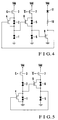
- Fig. 1 shows the first embodiment of the present invention. Referring to Fig. 1, this periodic waveform generating circuit is constituted as follows.
- the emitter electrode of a negative differential resistive element 1 is grounded.
- the collector electrode of the negative differential resistive element 1 is connected to the emitter electrode of a negative differential resistive element 2.
- the collector electrode of the negative differential resistive element 2 is connected to the source electrode of a field-effect transistor 3.
- the drain electrode of the field-effect transistor 3 is connected to a power supply.
- the source electrode of a field-effect transistor 4 is connected to the emitter electrode of the negative differential resistive element 1.
- the drain electrode of the field-effect transistor 4 is connected to the collector electrode of the negative differential resistive element 1.
- the emitter electrode of a negative differential resistive element 5 is grounded.
- the collector electrode of the negative differential resistive element 5 is connected to the emitter electrode of a negative differential resistive element 6.
- the collector electrode of the negative differential resistive element 6 is connected to the source electrode of a field-effect transistor 7.
- the drain electrode of the field-effect transistor 7 is connected to a power supply.
- the source electrode of a field-effect transistor 8 is connected to the emitter electrode of the negative differential resistive element 5.
- the drain electrode of the field-effect transistor 8 is connected to the collector electrode of the negative differential resistive element 5. In this way, a second element circuit is constituted.
- An inverting element circuit is constituted by grounding the source electrode of a field-effect transistor 9, connecting the drain electrode of the field-effect transistor 9 to one terminal of a resistor 10, and connecting the other terminal of the resistor 10 to a power supply.
- the collector electrode of the negative differential resistive element 1 is connected to the gate electrode of the field-effect transistor 8.
- the collector electrode of the negative differential resistive element 5 is connected to the gate electrode of the field-effect transistor 9.
- the drain electrode of the field-effect transistor 9 is connected to the gate electrode of the field-effect transistor 4.
- This embodiment is operated as follows. That is, a high-frequency signal is input to the gate electrode of the field-effect transistor 3, and an inverted signal of that input signal is input to the gate electrode of the field-effect transistor 7. By outputting the potential at any of the collector electrode of the negative differential resistive element 1, the collector electrode of the negative differential resistive element 5, and the drain electrode of the field-effect transistor 9, a high frequency which is 1/2 the input high frequency is obtained as this output signal.
- rtd1 and rtd2 denote negative differential resistive elements; and fet1 and fet3, field-effect transistors.
- the current-voltage characteristics of a parallel circuit of rtd1 and fet1 and that of rtd2 are shown in Fig. 12A.
- the current-voltage characteristic of the parallel circuit of rtd1 and fet1 changes as shown in Fig. 12A in accordance with whether a potential V in of the gate electrode of fet1 is a high potential (H) or a low potential (L).
- element parameters are so selected that when the potential V in of the gate electrode of fet1 is the high potential (H), the peak current of the current-voltage characteristic of the parallel circuit of rtd1 and fet1 is larger than the peak current of rtd2, and that when the potential V in of the gate electrode of fet1 is the low potential (L), the peak current of the current-voltage characteristic of the parallel circuit of rtd1 and fet1 is smaller than the peak current of rtd2.
- a voltage region where negative differential characteristics appear is defined as a region II
- a positive voltage region whose voltage is lower than that in the region II is defined as a region I
- a region whose voltage is higher than that in the region II is defined as a region III.
- the operating point when V in is the low potential (L) is calculated by regarding fet3 of the circuit shown in Fig. 11 as a load resistance.
- Fig. 12B shows the current-voltage characteristics of a portion except fet3 of the circuit shown in Fig. 11 and those of fet3.
- the polygonal lines indicate the characteristics of the portion except fet3 of the circuit shown in Fig. 11, and the curves indicate the characteristics of fet3.
- the characteristics of fet3 are plotted as load curves when a power supply voltage Vd is 0.9 V.
- the thick straight lines indicate a stable state
- the thin straight lines indicate an unstable state.
- Curves 12 and 13 plot the characteristics of fet3 as load curves.
- the curve 12 is obtained when a gate potential Q of fet3 is the high potential (H)
- the curve 13 is obtained when the gate potential Q of fet3 is the low potential (L).
- the operating point is given by the intersection of a thick line and a curve. Therefore, when the gate potential Q of fet3 is the high potential (H), two operating points exist to result in a bistable state.
- the gate potential Q of fet3 is the low potential (L) only one operating point exists to result in a monostable state.
- V1 of the circuit in Fig. 11 in the bistable state when the gate potential Q of fet3 is the high potential (H) will be examined below.
- Fig. 13A shows V1 as a function of V2 in the circuit of Fig. 11. In the bistable state, V2 or a voltage applied to the portion except fet3 of the circuit in Fig. 11 is about 0.8 V as can be seen from Fig. 12B.
- Fig. 13A shows that when V2 is about 0.8 V, V1 is about 0.16 V (low potential, L) if the operating point is in branch [I,III] and about 0.6 V (high potential, H) if the operating point is in branch [III,I]. Accordingly, when the gate potential Q of fet3 is the high potential (H), V1 can be either the high potential (H) or the low potential (L).
- V in is the high potential (H)
- H high potential
- Figs. 13B and 13C A case where V in is the high potential (H) can be analyzed by similar discussions by using Figs. 13B and 13C. That is, when the gate potential Q of fet3 changes in order of H, L, H, L,..., V1 changes as shown in Table 3.
- Table 3 (When V in is high potential (H)) Q H L H L H L V1 (initial value is H) H L L L L L L V1 (initial value is L) L L L L L L L L L
- Figs. 12B and 13B also reveal that when the gate potential Q of fet3 is the high potential (H), V1 does not change even if V in changes from H to L or vice versa.
- the gate potential Q of fet3 is the low potential (L)
- V1 is always the low potential (L) regardless of the value of V in .
- the gate potential of the field-effect transistor 4 is equivalent to V in in the above discussions, and the collector potential of the negative differential resistive element 1 is equivalent to V1 in the above discussions. In this embodiment, however, the gate potential of the field-effect transistor 4 equals the potential at the drain electrode of the field-effect transistor 9.
- the gate potential of the field-effect transistor 8 is equivalent to V in in the above discussions, and the collector potential of the negative differential resistive element 5 is equivalent to V1 in the above discussions. In this embodiment, however, the gate potential of the field-effect transistor 8 equals the collector potential of the negative differential resistive element 1.
- the current path at the right end is a simple inverter. Accordingly, when the potential at the gate electrode of the field-effect transistor 9 is the high potential (H), the potential at the drain electrode of the field-effect transistor 9 is the low potential (L). When the potential at the gate electrode of the field-effect transistor 9 is the low potential (L), the potential at the drain electrode of the field-effect transistor 9 is the high potential (H).
- Figs. 14A to 14E the operation of this embodiment is shown in Figs. 14A to 14E.
- a high-frequency signal Q is input to the gate electrode of the field-effect transistor 3 and an inverted signal of that input signal is input to the gate electrode of the field-effect transistor 7, a high frequency which is 1/2 the input high frequency appears in any of the collector electrode of the negative differential resistive element 1, the collector electrode of the negative differential resistive element 5, and the drain electrode of the field-effect transistor 9.
- This embodiment operates as a 1/2 frequency divider. Since each state of the above circuit can be statically held, this embodiment is a 1/2 static frequency divider.
- a 1/2 static frequency divider is realized by using ten elements: four negative differential resistive elements, five field effect transistors, and a resistor.
- Fig. 49 one prior art necessitates 52 elements.
- This prior art requires 40 elements only in portions having functions equivalent to this embodiment, i.e., in an input buffer circuit and a toggle flip-flop circuit. That is, in this embodiment, the number of elements can be reduced to 1/4 to 1/5. Consequently, it is possible to increase the operating speed and reduce the consumption power.
- Fig. 2 shows the second embodiment of the present invention.
- This embodiment is the same as the first embodiment except the following point.
- the drain electrode of the field-effect transistor 9 is connected to one terminal of the resistor 10, and the other terminal of the resistor 10 is connected to the power supply.
- the other terminal of a resistor 10 is connected to the emitter of a level-shift diode 11, and the collector of the level-shift diode 11 is connected to a power supply.
- the characteristic feature of this embodiment is that the operation margin of the circuit is increased by the level-shift diode.
- the number of elements of this embodiment is 11, which is smaller than 40 to 52 in the prior art.
- Fig. 3 shows the third embodiment of the present invention.
- the source electrode of the field-effect transistor 4 is connected to the emitter electrode of the negative differential resistive element 1.
- the drain electrode of the field-effect transistor 4 is connected to the collector electrode of the negative differential resistive element 1.
- the source electrode of the field-effect transistor 8 is connected to the emitter electrode of the negative differential resistive element 5.
- the drain electrode of the field-effect transistor 8 is connected to the collector electrode of the negative differential resistive element 5.
- the source electrode of a field-effect transistor 4 is connected to the emitter electrode of a negative differential resistive element 2.
- the drain electrode of the field-effect transistor 4 is connected to the collector electrode of the negative differential resistive element 2.
- the source electrode of a field-effect transistor 8 is connected to the emitter electrode of a negative differential resistive element 6.
- the drain electrode of the field-effect transistor 8 is connected to the collector electrode of the negative differential resistive element 6.
- Fig. 4 shows the fourth embodiment of the present invention.
- This embodiment is the same as the third embodiment except the following point.
- the drain electrode of the field-effect transistor 9 is connected to one terminal of the resistor 10, and the other terminal of the resistor 10 is connected to the power supply.
- the other terminal of a resistor 10 is connected to the emitter of a level-shift diode 11, and the collector of the level-shift diode 11 is connected to a power supply.
- the third and fourth embodiments of the present invention are obtained by slightly modifying the first and second embodiments, respectively. That is, in the first and second embodiments, the field-effect transistors to be connected in parallel with the negative differential resistive elements are arranged in parallel with the first and third negative differential resistive elements, i.e., the negative differential resistive elements in the first stage from the ground. In the third and fourth embodiments, the field-effect transistors to be connected in parallel with the negative differential resistive elements are arranged in parallel with the second and fourth negative differential resistive elements, i.e., the negative differential resistive elements in the second stage from the ground.
- This circuit configuration can also accomplish the function of a 1/2 static frequency divider.
- Fig. 5 shows the fifth embodiment of the present invention.
- the emitter electrode of a negative differential resistive element 1 is grounded.
- the collector electrode of the negative differential resistive element 1 is connected to the emitter electrode of a negative differential resistive element 2.
- the collector electrode of the negative differential resistive element 2 is connected to the source electrode of a field-effect transistor 3.
- the drain electrode of the field-effect transistor 3 is connected to a power supply.
- the source electrode of a field-effect transistor 4 is connected to the emitter electrode of the negative differential resistive element 1.
- the drain electrode of the field-effect transistor 4 is connected to the collector electrode of the negative differential resistive element 1.
- the emitter electrode of a negative differential resistive element 5 is grounded.
- the collector electrode of the negative differential resistive element 5 is connected to the emitter electrode of a negative differential resistive element 6, and the collector electrode of the negative differential resistive element 6 is connected to the source electrode of a field-effect transistor 7.
- the drain electrode of the field-effect transistor 7 is connected to a power supply.
- the source electrode of a field-effect transistor 8 is connected to the emitter electrode of the negative differential resistive element 6.
- the drain electrode of the field-effect transistor 8 is connected to the collector electrode of the negative differential resistive element 6.
- the collector electrode of the negative differential resistive element 1 is connected to the gate electrode of the field-effect transistor 8.
- the collector electrode of the negative differential resistive element 5 is connected to the gate electrode of the field-effect transistor 4.
- This embodiment is operated as follows. A high-frequency signal is applied to the gate electrode of the field-effect transistor 3, and an inverted signal of that input signal is applied to the gate electrode of the field-effect transistor 7. The potential at either the collector electrode of the negative differential resistive element 1 or the collector electrode of the negative differential resistive element 5 is extracted as an output signal.
- the operation of this embodiment is shown in Figs. 15A to 15D. It is evident from Figs. 15A to 15D that this circuit operates as a 1/2 frequency divider. Since each state of the circuit of this embodiment can be statically held, this embodiment is a 1/2 static frequency divider.
- the field-effect transistors to be connected in parallel with the negative differential resistive elements are arranged in parallel with the first and fourth negative differential resistive elements, i.e., the negative differential resistive element in the first stage from the ground on the left-side current path and the negative differential resistive element in the second state from the ground on the right-side current path.
- This obviates the need for the inverter provided as the current path at the right end in each of the first to fourth embodiments.
- This further reduces the number of elements to 8 which is smaller than in the first to fourth embodiments. Consequently, it is possible to further increase the operating speed and reduce the consumption power.
- the collector electrode of the negative differential resistive element 2 is connected to the source electrode of the field-effect transistor 3.
- the collector electrode of the negative differential resistive element 6 is connected to the source electrode of the field-effect transistor 7.
- the function of the field-effect transistor 3 is to determine the potential at the collector electrode of the negative differential resistive element 2 in accordance with the potential Q at the gate electrode of the field-effect transistor 3.
- the function of the field-effect transistor 7 is to determine the potential at the collector electrode of the negative differential resistive element 6 in accordance with the potential Q at the gate electrode of the field-effect transistor 7.
- Table 4 Q Potential at collector electrode of second negative differential resistive element 2 Potential at collector electrode of fourth negative differential resistive element 6 H H L L L L H
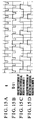
- Figs. 16 to 20 illustrate the 11th to 15th embodiments, respectively, of the present invention in which the field-effect transistors 3 and 7 used in the first to fifth embodiments are removed and, instead, the collector electrodes of negative differential resistive elements 2 and 6 are connected to power supply circuits.
- Table 5 is identical with Table 4. This demonstrates that the 11th to 15th embodiments of this circuit operate in the same manner as the first to fifth embodiments, respectively, of the circuit.
- the 11th to 15th embodiments of this circuit use the power supply circuit in which the resistor 14, the field-effect transistors 15 and 16, the resistor 17, and the power supply are connected as shown in Figs. 16 to 20.
- any other power supply circuit can also be used, provided that the input signal Q and the potentials at the individual collector electrodes meet the relationships shown in Table 4.
- Fig. 6 shows the sixth embodiment of the present invention.
- the source electrode of a field-effect transistor 3 is grounded.
- the drain electrode of the field-effect transistor 3 is connected to the emitter electrode of a negative differential resistive element 1.
- the collector electrode of the negative differential resistive element 1 is connected to the emitter electrode of a negative differential resistive element 2.
- the collector electrode of the negative differential resistive element 2 is connected to a power supply.
- the source electrode of a field-effect transistor 4 is connected to the emitter electrode of the negative differential resistive element 1.
- the drain electrode of the field-effect transistor 4 is connected to the collector electrode of the negative differential resistive element 1.
- the source electrode of a field-effect transistor 7 is grounded.
- the drain electrode of the field-effect transistor 7 is connected to the emitter electrode of a negative differential resistive element 5.
- the collector electrode of the negative differential resistive element 5 is connected to the emitter electrode of a negative differential resistive element 6.
- the collector electrode of the negative differential resistive element 6 is connected to a power supply.
- the source electrode of a field-effect transistor 8 is connected to the emitter electrode of the negative differential resistive element 5.
- the drain electrode of the field-effect transistor 8 is connected to the collector electrode of the negative differential resistive element 5.
- the source electrode of a field-effect transistor 9 is grounded.
- the drain electrode of the field-effect transistor 9 is connected to one terminal of a resistor 10.
- the other terminal of the resistor 10 is connected to a power supply.
- the collector electrode of the negative differential resistive element 1 is connected to the gate electrode of the field-effect transistor 8.
- the collector electrode of the negative differential resistive element 5 is connected to the gate electrode of the field-effect transistor 9.
- the drain electrode of the field-effect transistor 9 is connected to the gate electrode of the field-effect transistor 4.
- Fig. 7 shows the seventh embodiment of the present invention. This embodiment is the same as the sixth embodiment except the following point.
- the source electrode of the field-effect transistor 9 is grounded.
- the emitter of a level-shift diode 11 is grounded, and the collector of the level-shift diode 11 is connected to the source electrode of a field-effect transistor 9.
- Fig. 8 shows the eighth embodiment of the present invention.
- This embodiment is the same as the sixth embodiment except the following point.
- the source electrode of the field-effect transistor 4 is connected to the emitter electrode of the negative differential resistive element 1.
- the drain electrode of the field-effect transistor 4 is connected to the collector electrode of the negative differential resistive element 1.
- the source electrode of the field-effect transistor 8 is connected to the emitter electrode of the negative differential resistive element 5.
- the drain electrode of the field-effect transistor 8 is connected to the collector electrode of the negative differential resistive element 5.
- the source electrode of a field-effect transistor 4 is connected to the emitter electrode of a negative differential resistive element 2.
- the drain electrode of the field-effect transistor 4 is connected to the collector electrode of the negative differential resistive element 2.
- the source electrode of a field-effect transistor 8 is connected to the emitter electrode of a negative differential resistive element 6.
- the drain electrode of the field-effect transistor 8 is connected to the collector electrode of the negative differential resistive element 6.
- Fig. 9 shows the ninth embodiment of the present invention. This embodiment is the same as the eighth embodiment except the following point.
- the source electrode of the field-effect transistor 9 is grounded.
- the emitter electrode of a level-shift diode 11 is grounded, and the collector electrode of the level-shift diode 11 is connected to the source electrode of a field-effect transistor 9.
- Fig. 10 shows the 10th embodiment of the present invention.
- This embodiment is the same as the fifth embodiment except the following point.
- the emitter electrode of the negative differential resistive element 1 is grounded.
- the collector electrode of the negative differential resistive element 2 is connected to the source electrode of the field-effect transistor 3.
- the drain electrode of the field-effect transistor 3 is connected to the power supply.
- the emitter electrode of the negative differential resistive element 5 is grounded.
- the collector electrode of the negative differential resistive element 6 is connected to the source electrode of the field-effect transistor 7.
- the drain electrode of the field-effect transistor 7 is connected to the power supply.
- the source electrode of a field-effect transistor 3 is grounded.
- the drain electrode of the field-effect transistor 3 is connected to the emitter electrode of a negative differential resistive element 1.
- the collector electrode of a negative differential resistive element 2 is connected to a power supply.
- the source electrode of a field-effect transistor 7 is grounded.
- the drain electrode of the field-effect transistor 7 is connected to the emitter electrode of a negative differential resistive element 5.
- the collector electrode of a negative differential resistive element 6 is connected to a power supply.
- the sixth to 10th embodiments are obtained by slightly modifying the first to fifth embodiments, respectively. That is, in the first to fifth embodiments, the field-effect transistors to be connected in series with the negative differential resistive elements are connected on the power supply side. In the sixth to 10th embodiments, these field-effect transistors are connected on the ground side. This circuit configuration can also realize a 1/2 frequency dividing operation in the same manner as in the first to fifth embodiments.
- Figs. 21 to 25 illustrate the 16th to 20th embodiments of the circuit of the present invention in which the field-effect transistors 3 and 7 in the sixth to 10th embodiments are removed and, instead, the source electrodes of negative differential resistive elements 1 and 5 are connected to power supply circuits.
- this power supply circuit When applied with an input signal Q, this power supply circuit generates the same potential as generated in the source electrodes of the negative differential resistive elements 1 and 5 in the sixth to 10th embodiments in the source electrodes of the negative differential resistive elements 1 and 5 in the 16th to 20th embodiments.
- the 16th to 20th embodiments operate in the same manner as the sixth to 10th embodiments. That is, each embodiment operates as a 1/2 frequency divider.
- a resonant tunnel diode consisting of an n-type InGaAs semiconductor layer as the emitter and the collector and an undoped AlAs semiconductor layer as the barrier layer can be used as each negative differential resistive element. It is also possible to use an Esaki diode as the negative differential resistive element. Furthermore, any device, regardless of whether the device is a single element or circuit, can be used as the negative differential resistive element of the present invention as long as the device has negative differential resistance characteristics.
- any device such as a metal thin film resistor, a semiconductor thin film resistor, or a field-effect transistor in which the gate electrode and the source electrode are connected, can be used as the resistor of the present invention, provided that the device causes a voltage drop when a current flows.
- Fig. 26 shows the 21st embodiment of the present invention. This embodiment comprises first element circuits 20, 22, 24,..., second element circuits 21, 23, 25,..., and an inverting element circuit 26.
- SC1 denotes a first element circuit
- SC2 a second element circuit. -0,..., -N following these reference symbols indicate the ordinal numbers.
- the first element circuit consists of negative differential resistive elements 27 and 28 and a field-effect transistor 29.
- the emitter electrode of the negative differential resistive element 27 is connected to ground 30.
- a collector electrode 31 (also called a node) of the negative differential resistive element 28 is connected to a first power supply.
- the collector electrode of the negative differential resistive element 27 is connected to the emitter electrode of the negative differential resistive element 28.
- the source and drain electrodes of the field-effect transistor 29 are connected to the emitter and collector electrodes, respectively, of the negative differential resistive element 27.
- the potential at the gate electrode of the field-effect transistor 29 is an input 32.
- the potential at the collector electrode of the negative differential resistive element 27 is an output 33.
- the second element circuit is the same as the first element circuit except that the collector of the negative differential resistive element 28 in the first element circuit is connected to a second power supply.
- This embodiment includes the same numbers ((N+1) in Fig. 26; N is a non-negative integer) of the first element circuits and the second element circuits and one inverting element circuit.
- the output of the first element circuit SC1-0 is connected to the input of the second element circuit 21,
- the potential at the output terminal of the inverting element circuit is output.
- the principle of operation of this embodiment will be described below.
- the first element circuit is easy to understand when it is divided into a driver unit 36 and a load unit 37 as shown in Fig. 30.
- the driver unit is a parallel connection of a resonant tunneling diode and a field-effect transistor. Therefore, the driver current changes in accordance with an input V in to the gate electrode of the field-effect transistor.
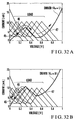
- Fig. 31A shows the current-voltage characteristics of the driver and the load. What is important is that individual element parameters are so set that, as shown in Fig.
- a peak current 38 of the driver when the input V in to the gate electrode of the field-effect transistor is H is larger than a peak current 39 of the load
- a peak current 40 of the driver when the input V in to the gate electrode of the field-effect transistor is L is smaller than the peak current 39 of the load.
- the operating point of this element circuit is uniquely given as the intersection of the current-voltage characteristics of the driver and the load as indicated by reference symbol ⁇ 42 in Fig. 31B.
- the operating point of this element circuit can take two values 43 and 44 as indicated by reference symbols o in Fig. 31B. Assume that the applied voltage at that time is H. Whether the operating point takes the value 43 or 44 is determined by the past history as will be explained below. In this embodiment, this function of the element circuit is used to temporarily store information.
- Fig. 32B shows the change of the operating point when the input 32 to this element circuit is H.
- the peak current in the driver unit is larger than that in the load unit.
- Fig. 32B plots the current-voltage characteristic of the driver unit and the load curves of the load unit corresponding to several applied voltages to the node 31.
- the operating point moves in a complicated manner; it moves from the point 45 to the right as the applied voltage increases but returns to the left in the middle of the movement.
- the left-side one of two operating points is selected. This accomplishes a state in which a low voltage is applied to the driver unit and a high voltage is applied to the load unit. That is, L is output to the output 33. This is because the peak current in the driver unit is larger than that in the load unit, so the voltage applied to the driver unit is always lower than the peak voltage.
- Fig. 32D shows the load curve of this element circuit in this case.
- Fig. 34 shows the timing chart of this element circuit shown in Fig. 33.
- the output is always the low potential L.
- V out when the input V in changes, a change in the input has no effect on the output.
- CLK is at the high potential H and the input changes. If this is the case, as described in item (2) above, the output maintains the value immediately before the input changes.
- reference symbols t 1 to t 6 denote times at which CLK changes from the low potential L to the high potential H.
- the input is at the high potential H, so the output is at the low potential L as described in item (3) above.
- the input is at the low potential L, so the output is at the high potential H as described in item (3).
- the first element circuits and the second element circuits are alternately arranged.
- the first element circuits are given even-number indices, and their outputs are represented by A 0 , A 2 ,..., A 2N .
- the second element circuits are given odd-number indices, and their outputs are represented by A 1 , A 3 ,..., A 2N+1 .
- the input potentials to the first element circuits are represented by a 0 , a 2 ,..., a 2N .
- the input potentials to the second element circuits are represented by a 1 , a 3 ,..., a 2N+1 .
- the first power supply or the clock CLK and the second power supply or a clock bar CLK ⁇ are indexed as shown in Figs. 36A and 36B.
- a value of more than 50% is chosen as the duty ratios of the clock pulse and the clock bar pulse to set a time period during which the clock and the clock bar are simultaneously at the high potential H. This is done for the sake of convenience of explanation and is not necessarily essential as will be described later.
- the output potential and the input potential of an element circuit k at time m are represented by A(k,m) and a(k,m), respectively.
- Equations [23] and [24] hold due to the dynamics of the first and second element circuits.
- A(2k,2n+1) 1 - a(2k,2n)
- A(2k+1,2n) 1 - a(2k+1,2n-1)
- Equation [23] indicates that the inversion of an input a(2k,2n) to the first element circuit is an output A(2k,2n+1) of that element circuit at leading edges 66 and 69 of the clock shown in Fig. 36A.
- Equation [24] indicates that the inversion of an input a(2k+1,2n-1) to the second element circuit is an output A(2k+1,2n) of that element circuit at leading edges 67 and 68 of the clock bar shown in Fig. 36B.
- Equation [27] shows that all node potentials in the form of A(2k,2n+1) are reduced into the form of A(0,2p+1).
- an equation containing only terms in the form of A(0,2p+1) is derived and solved to obtain a practical solution of A(0,2p+1).
- Equation [30] is obtained by matching time 2n on the right side with 2n+1 on the left side by using the relationship of equation [25] and rearranging the result by equation [27].
- A(0,2(n+N+1)+1) 1 - A(0,2n+1)
- Equation [30] is related to A(0,2p+1), and practical solution [31] can be obtained.
- A(0,2m+1) (-1) ⁇ INT((2m+1)/2/(N+1))* (A(0,MOD(2m+1,2N+2) - 0.5) + 0.5
- INT(x) is a maximum integer not exceeding x
- MOD(x,y) is a remainder when x is divided by y.
- Equation [31] contains N parameters A(0,1), A(0,3), A(0,5),..., A(0,2N+1). These parameters are initial values (or boundary conditions) of this equation.
- a more general solution A(2k,2n+1) can be written as equation [32] by using equation [27].
- A(2k,2n+1) is found to be a periodic function which inverts at a time interval of 2N+2 and has a period of 2*(2N+2).
- the clock period is 2 as shown in Fig. 36A. Therefore, the output A(2k,2n+1) of the element circuit with index 2k of this embodiment is a periodic function whose period is (2N+2) times the clock. Also, equation [33] shows that A(2k+1,2n) has the same period as A(2k,2n+1). This demonstrates that this embodiment is a 1/(2N+2) frequency dividing circuit assuming the order of the circuit is N.
- frequency dividers of ratios 1/2, 1/4, 1/6, 1/8, 1/10,... can be manufactured with a simple arrangement by selecting 0, 1, 2, 3, 4,..., as N.
- the above discussions do not use practical initial conditions (or boundary conditions). Accordingly, the above conclusion generally holds for the first embodiment regardless of the initial conditions.
- Figs. 40, 41, 42, and 43 illustrate the calculation results of this embodiment when the order N of the circuit is 0, 1, 2, and 3. Calculations were performed for outputs of all element circuits contained in the circuit.
- all initial values contained in equation [31] are 0.
- the calculation result of the output of each element circuit is such that the period of the output is 2*(N+1) times the clock, i.e., the output frequency is 1/(2N+2) times the clock.
- the output from each element circuit is a string of (N+1) pulses whose pulse width is equal to that of the clock pulse.
- ORing A0 and A5 yields a pulse string whose period is six times (2*(N+1)) the clock and duty ratio is 50%. Furthermore, it is possible to arrange a plurality of circuits of this embodiment and perform logical operations for outputs from individual element circuits.
- Fig. 28 shows the 22nd embodiment of the present invention.
- the above 21st embodiment includes only the first and second element circuits as element circuits.
- This 22nd embodiment includes third and fourth element circuits in addition to the first and second element circuits.
- the sum of the numbers of the first and third element circuits equals the sum of the numbers of the second and fourth element circuits.
- the sum of the numbers of the third and fourth element circuits and an inverting element circuit must be an odd number.
- the third element circuit is identical with the first element circuit except the following point. That is, the source and drain electrodes of a field-effect transistor are connected to the emitter and collector electrodes, respectively, of a second negative differential resistive element. In the first element circuit, these electrodes are connected to the first negative differential resistive element, and this is the difference.
- the fourth element circuit is identical with the second element circuit except the following point. That is, the source and drain electrodes of a field-effect transistor are connected to the emitter and collector electrodes, respectively, of a second negative differential resistive element. In the second element circuit, these electrodes are connected to the first negative differential resistive element, and this is the difference.
- Table 6 First element circuit Second element circuit Third element circuit Fourth element circuit Power supply First power supply Second power supply First power supply Second power supply Parallel field-effect transistor First NDR element First NDR element Second NDR element Second NDR element Second NDR element Second NDR element
- the 22nd embodiment shown in Fig. 28 includes one fourth element circuit 21' and one third element circuit 24'. Equations describing the operation of the 21st embodiment are equations [17] to [24]. Equations describing this embodiment are the same as the 21st embodiment except that equations [23] and [24] are replaced with equations [36] and [37], respectively.
- equations [38] to [43] are obtained.
- A(0,2n+1) (-1) ⁇ INT((2n+1)/6)* (A(0,MOD(2n+1,6) - 0.5) + 0.5
- A(1,2n) A(0,2n-1)
- A(2,2n+1) 1 - A(0,2n-1)
- A(3,2n) A(0,2n-3)
- A(4,2n+1) A(0,2n-3)
- A(5,2n) A(0,2n+1)
- Fig. 29 shows the 23rd embodiment of the present invention. This embodiment is mostly the same as the second embodiment except that no inverting element circuit is included. The sum of the numbers of first and third element circuits is made equal to the sum of the numbers of second and fourth element circuits. The sum of the numbers of the third and fourth element circuits must be an odd number. In the embodiment shown in Fig. 29, one third element circuit 24' and two fourth element circuits 21' and 23' are used. Analysis analogous to those in the first and second embodiments shows that this embodiment is also a periodic function which inverts at a time interval of (2N+2) and has a period of 2*(2N+2).
- the outputs of the element circuits with indices 0 and 3 in the 23rd embodiment equal those in the 21st embodiment and the outputs of the element circuits with indices 1, 2, 4, and 5 in the 23rd embodiment equal the inversions of the respective counterparts in the 21st embodiment.
- the outputs in the 21st and 22nd embodiments will be compared below. These two embodiments have the same outputs in the element circuits at the positions of indices 0 4, and 5. However, the outputs in one embodiment are the inversions of the outputs in the other in the element circuits at the positions of indices 1, 2, and 3. This accords with Table 7.
- the 21st and 23rd embodiments also have output differences corresponding to Table 7 because the 23rd embodiment includes the third and fourth element circuits.
- Figs. 44, 45, and 46 illustrate the calculation results of the operations of the 21st, 22nd, and 23rd embodiments (Fig. 44 is identical with Fig. 42). In Figs.
- Fig. 45 shows that the element circuits with indices 1, 2, and 3 in the 22nd embodiment output the inversions of the outputs of the respective counterparts in the 21st embodiment.
- This element circuit outputs 1 at times 2, 4, and 6. However, the same element circuit outputs 0 at the same times in the 22nd embodiment. On the other hand, at times 8, 10, and 1 at which 0 is output in the 21st embodiment, 1 is output in the 22nd embodiment.
- Figs. 44, 45, 46, and 47 also illustrate examples of the results of logical operations on outputs of the individual element circuits in these embodiments.
- various pulse strings can also be obtained in the 22nd and 23rd embodiments as in the 21st embodiment.
- an element circuit logical operation method for this purpose in one embodiment is not necessarily the same as in another.
- the phase of a pulse string differs from one embodiment to another. Accordingly, these embodiments can be used to obtain pulse strings having different phases.
- circuit shown in Fig. 28 is merely one example of the 22nd embodiment. Therefore, the numbers of the third and fourth element circuits and their positions are, of course, not limited by the example in Fig. 28.
- circuit shown in Fig. 29 is merely one example of the 23rd embodiment, so the numbers of the third and fourth element circuits and their positions are not limited by the example in Fig. 29.
- Figs. 48A, 48B, and 48C show abstracted circuits of the first to 23rd embodiments described above.
- reference numeral 70 denotes a first element circuit; 71, a fourth element circuit; 72, a first element circuit; 73, a second element circuit; 74, a third element circuit; 75, a second element circuit; 76, an inverting element circuit; 77, a first partial circuit; 78, a power supply terminal of the first partial circuit; 79, an input terminal of the first partial circuit; 80, an output terminal of the first partial circuit; 81, a second partial circuit; 82, a power supply terminal of the second partial circuit; 83, an input terminal of the second partial circuit; and 84, an output terminal of the second partial circuit.
- the input and output terminals are also referred to as an input and an output, respectively, and the power supply terminal is also referred to as a power supply.
- the basic operation of the first partial circuit 77 is as follows.
- the sum of the numbers of the first and third element circuits and the sum of the numbers of the second and fourth element circuits are equally (N+1) (N is a non-negative integer).
- the sum of the numbers of the third and fourth element circuits and the inverting element circuit is an odd number.
- One electrical group is formed by connecting the outputs and inputs of the first to fourth element circuits and the inverting element circuit. As described previously, if only the first and second partial circuits meet the above conditions, the above function can be achieved regardless of practical methods of constituting the individual partial circuits.
- a high-mobility field-effect transistor having an undoped InGaAs semiconductor layer as a channel layer and an InAlAs layer as a barrier layer can be used as each field-effect transistor.
- any transistor which operates as a field-effect transistor e.g., a metal-semiconductor field-effect transistor (MESFET) or a junction gate field-effect transistor (JFET) can be used as the field-effect transistor of the present invention.
- a bipolar transistor can be used instead of a field-effect transistor.
- the same voltage Vdd is applied to each power supply terminal.
- the applied power supply voltage can also be changed from one power supply terminal to another.
- the present invention makes use of the functionality of an element having negative differential resistance characteristics and realizes a function of generating various pulse strings from a clock signal with a smaller number of elements and a simpler circuit configuration than in conventional techniques. This reduces the consumption power and increases the operating speed of the circuit.
Landscapes
- Logic Circuits (AREA)
- Electronic Switches (AREA)
- Manipulation Of Pulses (AREA)
Applications Claiming Priority (6)
| Application Number | Priority Date | Filing Date | Title |
|---|---|---|---|
| JP8217896 | 1996-04-04 | ||
| JP82178/96 | 1996-04-04 | ||
| JP8217896 | 1996-04-04 | ||
| JP34197596A JP3508809B2 (ja) | 1996-04-04 | 1996-12-20 | 波形発生回路 |
| JP34197596 | 1996-12-20 | ||
| JP341975/96 | 1996-12-20 |
Publications (3)
| Publication Number | Publication Date |
|---|---|
| EP0800272A2 true EP0800272A2 (fr) | 1997-10-08 |
| EP0800272A3 EP0800272A3 (fr) | 1999-04-21 |
| EP0800272B1 EP0800272B1 (fr) | 2004-06-30 |
Family
ID=26423191
Family Applications (1)
| Application Number | Title | Priority Date | Filing Date |
|---|---|---|---|
| EP97105559A Expired - Lifetime EP0800272B1 (fr) | 1996-04-04 | 1997-04-03 | Circuit générateur de forme de l'onde périodique |
Country Status (4)
| Country | Link |
|---|---|
| US (1) | US5770958A (fr) |
| EP (1) | EP0800272B1 (fr) |
| JP (1) | JP3508809B2 (fr) |
| DE (1) | DE69729679T2 (fr) |
Families Citing this family (28)
| Publication number | Priority date | Publication date | Assignee | Title |
|---|---|---|---|---|
| IL130901A (en) * | 1999-07-12 | 2004-12-15 | Technion Res & Dev Foundation | High power bipolar transistor with emitter current density limiter |
| US6362660B1 (en) * | 1999-07-13 | 2002-03-26 | Texas Instruments Incorporated | CMOS latch and register circuitry using quantum mechanical tunneling structures |
| US6518589B2 (en) | 2000-06-22 | 2003-02-11 | Progressant Technologies, Inc. | Dual mode FET & logic circuit having negative differential resistance mode |
| US6512274B1 (en) * | 2000-06-22 | 2003-01-28 | Progressant Technologies, Inc. | CMOS-process compatible, tunable NDR (negative differential resistance) device and method of operating same |
| US6724655B2 (en) * | 2000-06-22 | 2004-04-20 | Progressant Technologies, Inc. | Memory cell using negative differential resistance field effect transistors |
| US6596617B1 (en) | 2000-06-22 | 2003-07-22 | Progressant Technologies, Inc. | CMOS compatible process for making a tunable negative differential resistance (NDR) device |
| US6754104B2 (en) * | 2000-06-22 | 2004-06-22 | Progressant Technologies, Inc. | Insulated-gate field-effect transistor integrated with negative differential resistance (NDR) FET |
| US6594193B2 (en) | 2000-06-22 | 2003-07-15 | Progressent Technologies, Inc. | Charge pump for negative differential resistance transistor |
| US6559470B2 (en) | 2000-06-22 | 2003-05-06 | Progressed Technologies, Inc. | Negative differential resistance field effect transistor (NDR-FET) and circuits using the same |
| US6479862B1 (en) * | 2000-06-22 | 2002-11-12 | Progressant Technologies, Inc. | Charge trapping device and method for implementing a transistor having a negative differential resistance mode |
| US7453083B2 (en) * | 2001-12-21 | 2008-11-18 | Synopsys, Inc. | Negative differential resistance field effect transistor for implementing a pull up element in a memory cell |
| US6894327B1 (en) | 2001-12-21 | 2005-05-17 | Progressant Technologies, Inc. | Negative differential resistance pull up element |
| US6912151B2 (en) * | 2002-06-28 | 2005-06-28 | Synopsys, Inc. | Negative differential resistance (NDR) based memory device with reduced body effects |
| US6795337B2 (en) | 2002-06-28 | 2004-09-21 | Progressant Technologies, Inc. | Negative differential resistance (NDR) elements and memory device using the same |
| US6567292B1 (en) | 2002-06-28 | 2003-05-20 | Progressant Technologies, Inc. | Negative differential resistance (NDR) element and memory with reduced soft error rate |
| US7098472B2 (en) * | 2002-06-28 | 2006-08-29 | Progressant Technologies, Inc. | Negative differential resistance (NDR) elements and memory device using the same |
| US7095659B2 (en) * | 2002-06-28 | 2006-08-22 | Progressant Technologies, Inc. | Variable voltage supply bias and methods for negative differential resistance (NDR) based memory device |
| US6853035B1 (en) | 2002-06-28 | 2005-02-08 | Synopsys, Inc. | Negative differential resistance (NDR) memory device with reduced soft error rate |
| US6847562B2 (en) * | 2002-06-28 | 2005-01-25 | Progressant Technologies, Inc. | Enhanced read and write methods for negative differential resistance (NDR) based memory device |
| US6864104B2 (en) * | 2002-06-28 | 2005-03-08 | Progressant Technologies, Inc. | Silicon on insulator (SOI) negative differential resistance (NDR) based memory device with reduced body effects |
| US6806117B2 (en) * | 2002-12-09 | 2004-10-19 | Progressant Technologies, Inc. | Methods of testing/stressing a charge trapping device |
| US6979580B2 (en) * | 2002-12-09 | 2005-12-27 | Progressant Technologies, Inc. | Process for controlling performance characteristics of a negative differential resistance (NDR) device |
| US7012833B2 (en) * | 2002-12-09 | 2006-03-14 | Progressant Technologies, Inc. | Integrated circuit having negative differential resistance (NDR) devices with varied peak-to-valley ratios (PVRs) |
| US6849483B2 (en) * | 2002-12-09 | 2005-02-01 | Progressant Technologies, Inc. | Charge trapping device and method of forming the same |
| US6980467B2 (en) * | 2002-12-09 | 2005-12-27 | Progressant Technologies, Inc. | Method of forming a negative differential resistance device |
| US6812084B2 (en) * | 2002-12-09 | 2004-11-02 | Progressant Technologies, Inc. | Adaptive negative differential resistance device |
| US7005711B2 (en) * | 2002-12-20 | 2006-02-28 | Progressant Technologies, Inc. | N-channel pull-up element and logic circuit |
| WO2013062595A1 (fr) * | 2011-10-28 | 2013-05-02 | Hewlett-Packard Development Company, L.P. | Flip-flop à transition de phase métal-isolant |
Family Cites Families (8)
| Publication number | Priority date | Publication date | Assignee | Title |
|---|---|---|---|---|
| DE1168964B (de) * | 1961-05-31 | 1964-04-30 | Intermetall | Schaltungsanordnung zum binaeren Zaehlen oder zum Frequenzteilen |
| DE1438459A1 (de) * | 1961-11-20 | 1968-10-17 | Itt Ind Gmbh Deutsche | Drehstromgenerator fuer in weiten Grenzen einstellbare Frequenzen |
| GB1320379A (en) * | 1969-09-19 | 1973-06-13 | Matsushita Electric Industrial Co Ltd | Circuit arrangement utilizing oscillatory diode |
| US3740576A (en) * | 1970-08-04 | 1973-06-19 | Licentia Gmbh | Dynamic logic interconnection |
| US4553047A (en) * | 1983-01-06 | 1985-11-12 | International Business Machines Corporation | Regulator for substrate voltage generator |
| US5313117A (en) * | 1991-07-22 | 1994-05-17 | Nippon Telegraph And Telephone Corporation | Semiconductor logic circuit using two n-type negative resistance devices |
| US5479129A (en) * | 1993-11-24 | 1995-12-26 | At&T Corp. | Variable propagation delay digital signal inverter |
| JP2970389B2 (ja) * | 1994-03-30 | 1999-11-02 | 日本電気株式会社 | フリップ・フロップ回路 |
-
1996
- 1996-12-20 JP JP34197596A patent/JP3508809B2/ja not_active Expired - Fee Related
-
1997
- 1997-04-01 US US08/831,995 patent/US5770958A/en not_active Expired - Lifetime
- 1997-04-03 DE DE69729679T patent/DE69729679T2/de not_active Expired - Lifetime
- 1997-04-03 EP EP97105559A patent/EP0800272B1/fr not_active Expired - Lifetime
Also Published As
| Publication number | Publication date |
|---|---|
| JPH09326677A (ja) | 1997-12-16 |
| EP0800272A3 (fr) | 1999-04-21 |
| DE69729679T2 (de) | 2005-07-21 |
| DE69729679D1 (de) | 2004-08-05 |
| US5770958A (en) | 1998-06-23 |
| EP0800272B1 (fr) | 2004-06-30 |
| JP3508809B2 (ja) | 2004-03-22 |
Similar Documents
| Publication | Publication Date | Title |
|---|---|---|
| EP0800272A2 (fr) | Circuit générateur de forme de l'onde périodique | |
| US5955912A (en) | Multiplexer circuits | |
| US4395774A (en) | Low power CMOS frequency divider | |
| US4107549A (en) | Ternary logic circuits with CMOS integrated circuits | |
| US6191658B1 (en) | High speed coupled oscillator topology | |
| EP0330971A2 (fr) | Circuit de bascule | |
| JPH0211019A (ja) | 差動式電流スイッチ回路 | |
| US4749886A (en) | Reduced parallel EXCLUSIVE or and EXCLUSIVE NOR gate | |
| EP0626758A2 (fr) | Circuit dynamique adiabatique d'accentuation de précharge | |
| EP0238874B1 (fr) | Générateur de signaux temporels à résolution double de la fréquence d'horloge | |
| JPH0648779B2 (ja) | フリップフロップ回路 | |
| US4140924A (en) | Logic CMOS transistor circuits | |
| JPH11514164A (ja) | しきい値式によって表わすことができる論理エレメントを実現するための回路装置 | |
| US3928773A (en) | Logical circuit with field effect transistors | |
| US5477164A (en) | Adiabatic dynamic noninverting circuitry | |
| DEVI et al. | Energy reduction of D-flipflop using 130nm CMOS technology | |
| US7098697B2 (en) | Low voltage high-speed differential logic devices and method of use thereof | |
| US3555307A (en) | Flip-flop | |
| US20050280449A1 (en) | Apparatus and method for high frequency state machine divider with low power consumption | |
| EP0384000B1 (fr) | Circuit logique cascode en CMOS entièrement statique pour commutation de tension | |
| Ishii | Retiming gated-clocks and precharged circuit structures | |
| US5032741A (en) | CDCFL logic circuits having shared loads | |
| RU207051U1 (ru) | Устройство для контроля параллельного двоичного кода на чётность | |
| Biswas | State transition diagram for a pipeline unit based on single electron tunneling | |
| Hisakado et al. | Logically reversible arithmetic circuit using pass-transistor |
Legal Events
| Date | Code | Title | Description |
|---|---|---|---|
| PUAI | Public reference made under article 153(3) epc to a published international application that has entered the european phase |
Free format text: ORIGINAL CODE: 0009012 |
|
| AK | Designated contracting states |
Kind code of ref document: A2 Designated state(s): DE GB |
|
| PUAL | Search report despatched |
Free format text: ORIGINAL CODE: 0009013 |
|
| AK | Designated contracting states |
Kind code of ref document: A3 Designated state(s): DE GB |
|
| 17P | Request for examination filed |
Effective date: 19991021 |
|
| 17Q | First examination report despatched |
Effective date: 20020920 |
|
| GRAP | Despatch of communication of intention to grant a patent |
Free format text: ORIGINAL CODE: EPIDOSNIGR1 |
|
| GRAS | Grant fee paid |
Free format text: ORIGINAL CODE: EPIDOSNIGR3 |
|
| GRAA | (expected) grant |
Free format text: ORIGINAL CODE: 0009210 |
|
| AK | Designated contracting states |
Kind code of ref document: B1 Designated state(s): DE GB |
|
| REG | Reference to a national code |
Ref country code: GB Ref legal event code: FG4D |
|
| REF | Corresponds to: |
Ref document number: 69729679 Country of ref document: DE Date of ref document: 20040805 Kind code of ref document: P |
|
| PLBE | No opposition filed within time limit |
Free format text: ORIGINAL CODE: 0009261 |
|
| STAA | Information on the status of an ep patent application or granted ep patent |
Free format text: STATUS: NO OPPOSITION FILED WITHIN TIME LIMIT |
|
| 26N | No opposition filed |
Effective date: 20050331 |
|
| PGFP | Annual fee paid to national office [announced via postgrant information from national office to epo] |
Ref country code: GB Payment date: 20110228 Year of fee payment: 15 |
|
| PGFP | Annual fee paid to national office [announced via postgrant information from national office to epo] |
Ref country code: DE Payment date: 20110427 Year of fee payment: 15 |
|
| GBPC | Gb: european patent ceased through non-payment of renewal fee |
Effective date: 20120403 |
|
| PG25 | Lapsed in a contracting state [announced via postgrant information from national office to epo] |
Ref country code: GB Free format text: LAPSE BECAUSE OF NON-PAYMENT OF DUE FEES Effective date: 20120403 |
|
| REG | Reference to a national code |
Ref country code: DE Ref legal event code: R119 Ref document number: 69729679 Country of ref document: DE Effective date: 20121101 |
|
| PG25 | Lapsed in a contracting state [announced via postgrant information from national office to epo] |
Ref country code: DE Free format text: LAPSE BECAUSE OF NON-PAYMENT OF DUE FEES Effective date: 20121101 |